Introduction
X-ray techniques such as resonant inelastic-x-ray scattering (RIXS) Reference Schülke1,Reference Ament, van Veenendaal, Devereaux, Hill and van den Brink2 and nuclear resonant scattering (NRS) Reference Gerdau and DeWaard3 are powerful tools for examining the subtle aspects of material structure and dynamics. These techniques find applications in many fields of science ranging from fundamental physics to biophysics, chemistry, materials science, and other interdisciplinary fields, including geophysics and environmental sciences. For these versatile and increasingly popular x-ray techniques, the clarity of the results can be enhanced by improving the energy resolution, which is determined by the x-ray optics.
In the hard x-ray region (photon energies >∼5 keV), most high-energy-resolution optics use Bragg reflections in perfect crystals. For these energies, silicon has been the crystal of choice as it is readily available in large perfect crystals, has good mechanical and thermal properties, and its processing technology is well known. However, crystals other than silicon have the potential to provide high-energy resolutions (<∼10 meV) more easily and efficiently for some RIXS and NRS experiments. This article discusses nonsilicon optics with an emphasis on their potential to facilitate high-energy resolution. We do not make an optic-by-optic comparison to silicon designs, but instead qualitatively motivate the potential use of alternate materials. Our discussion focuses on single-reflection optics, but similar considerations can also apply to multireflection setups.
Optical issues
There are two major optical issues relevant to attaining high-energy resolution. First, the crystal quality must be good enough (e.g., sufficiently low dislocation density) to obtain the desired resolution. This can be seen through examination of Bragg’s Law (λ = 2d sin θ B ), which relates the wavelength of the x-rays (λ) and the spacing of the diffracting planes of the crystal (d) to the Bragg angle (θ B ). Thus, if dislocations and defects in the crystal lead to fluctuation in d-spacing (Δd), then the resolution as given by the fractional energy bandwidth (ε = |ΔE|/E = |Δλ|/λ) will be limited by the fractional variation of d-spacing (Δd/d). In order to achieve a resolution (ΔE) of 10 meV when measuring the energy (E) of 10 keV photons (ε = 10 meV/10 keV = 10–6), one needs an extremely well-ordered crystal with a lattice uniformity (Δd/d) better than 10–6. This will be discussed in more detail for several crystals.
The second major optical issue is the Bragg reflection’s tolerance to angular deviations of the incoming photon beam (i.e., angular acceptance). Differentiation of Bragg’s Law yields a relation between angular acceptance (ΔΘ) and fractional bandwidth (ε): ΔΘ = ε tan θ B . This means that for a Bragg angle that is far from 90°, attaining a fractional resolution of 10–6 requires parallel beams with divergence on the order of 1 μrad or better. On the other hand, typical x-ray beams have approximately 10 μrad divergence from the source and the desired collection of an analyzer crystal from a sample can be tens of mrad, much larger than the acceptance of most crystal Bragg reflections. However, when the Bragg angle is close to 90°—in a “backscattering” or “back-reflection” geometry—tan θ B is increased. This yields a much larger angular acceptance of the Bragg reflection, by several orders of magnitude. In other words, by designing the x-ray optics at or close to “backscattering,” the photon collection efficiency can be dramatically improved for a given energy resolution. Following Bragg’s Law (λ = 2d sin θ B ) with θ B = 90°, it is preferable to choose lattice planes satisfying d ≈ λ/2 when designing crystal optics.
The operating x-ray energy in RIXS or NRS is fixed by the scientific problem of interest—either by the core–shell electron binding energies for RIXS, or the nuclear resonance energies for NRS. In order to take advantage of the enhanced angular acceptance previously described, one should use a material with a lattice spacing d that is one-half of the corresponding wavelength. This issue motivates much of the interest in nonsilicon materials. Silicon and similar materials (e.g., diamond and germanium) with a highly symmetric cubic diamond structure (space group
 $\left[ {Fd\overline 3 m} \right]$
) offer rather limited sets of d-spacings to choose from. Nonsilicon materials, especially those with lower symmetry, can have many unique Bragg reflections over a given energy range, and are therefore more likely to have a backscattering reflection near a desired energy.
Reference Sutter, Baron, Ishikawa and Yamazaki4,Reference Yavaş, Ercan Alp, Sinn, Alataş, Said, Shvyd’ko, Toellner, Khachatryan, Billinge, Hasan and Sturhahn5
This is illustrated in
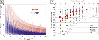
Figure 1a, where the minimum possible angular deviation from exact backscattering (θ
B
= 90°) is plotted as a function of x-ray energy for silicon (cubic) and quartz (trigonal). As can be seen, for high-symmetry silicon, the Bragg reflection deviates much further from backscattering than the lower symmetry quartz. Thus, lower-symmetry materials have a higher probability of a Bragg reflection near backscattering, gaining the benefit of large angular acceptance.
(a) Deviation from backscattering for silicon and quartz, and (b) bandwidth of selected reflections in the neighborhood of resonant inelastic x-ray scattering edges, where the size of the markers depicts the integrated reflectivity. Reference Gog, Casa, Said, Upton, Kim, Kuzmenko, Huang and Khachatryan6

Moreover, trigonal structures offer backscattering reflections with a wide range of bandwidths and reflectivities within a narrow band of x-ray energies, Reference Gog, Casa, Said, Upton, Kim, Kuzmenko, Huang and Khachatryan6 as seen in Figure 1b. This contrasts with silicon, germanium, and diamond, for which bandwidth ε = |ΔE/E| and reflectivity drop mostly monotonically as energy increases. Quartz offers superior resolution at low photon energies Reference Sutter, Baron, Miwa, Nishino, Tamasaku and Ishikawa7 because of its low Debye temperature, while sapphire, having a high Debye temperature, generally offers superior reflectivity at high energies. Reference Shvyd’ko, Gerdau, Jäschke, Leupold, Lucht and Rüter8 (In general, the reflectivity and bandwidth of Bragg reflections are not independent, and, furthermore, can depend significantly on the crystal temperature. The comments here are meant to be a rough guide.)
Finally, in addition to the optical concerns previously discussed, which can largely be addressed by careful calculations using dynamical diffraction principles, Reference Authier9 there are also important issues regarding the preservation of the desired response in the final optics (e.g., after the crystal is bent to a desired, usually spherical, shape) or when operating under heat load. This leads to an interesting practical materials fabrication problem on top of the x-ray optical problem.
Optical geometries
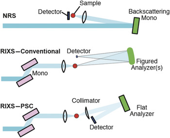
High-resolution nonsilicon optics are most interesting in three different geometries, as shown in Table I and Figure 2 . Reference Huotari, Vankó, Albergamo, Ponchut, Graafsma, Henriquet, Verbeni and Monaco10 The simplest geometry is a high-energy monochromator with high resolution, which is used for NRS measurements. The efficiency and angular acceptance of silicon reflections drop quickly above ∼25 keV, making single reflections from nonsilicon materials comparatively efficient, especially in sapphire. Reference Wille, Hermann, Sergueev, Pelzer, Möchel, Claudio, Perßon, Rüffer, Said and Shvyd’ko11,Reference Sergueev, Wille, Hermann, Bessas, Shvyd’ko, Zając and Rüffer12 The other two geometries are used to make analyzers for RIXS measurements. RIXS measurements rely on collecting a large solid angle of scattered x-rays from the sample (at least 10 × 10 mrad2, and often 100 × 100 mrad2 or more), making the large angular acceptance of back reflections appealing. One can make a figured optic (e.g., a spherical analyzer) or as shown more recently, Reference Shvyd’ko, Stoupin, Shu, Collins, Mundboth, Sutter and Tolkiehn13 collimate the divergent beam from the sample and use a flat crystal analyzer in a post-sample collimation (PSC) geometry; see discussion in Reference Reference Baron, Jaeschke, Khan, Schneider and Hastings14. Figured analyzers require relatively large crystals to be made Reference Yavaş, Ercan Alp, Sinn, Alataş, Said, Shvyd’ko, Toellner, Khachatryan, Billinge, Hasan and Sturhahn5,Reference Verbeni, Kocsis, Huotari, Krisch, Monaco, Sette and Vanko15,Reference Ketenoglu, Harder, Klementiev, Upton, Taherkhani, Spiwek, Dill, Wille and Yavaş16 (segmented, bent, or bonded) in order to achieve an appropriate curvature. These analyzers are also easily tiled, allowing large solid angles to be collected with potentially large arrays. On the other hand, the PSC scheme requires a collimating optic near the sample Reference Honnicke, Huang, Keister, Kodituwakku and Cai17–Reference Kim, Shi, Casa, Qian, Huang and Gog19 that, at present, usually cannot accept a large solid angle, and may be expensive to generate. However, only a relatively small analyzer crystal without any figuring is needed, which simplifies the analyzer fabrication process.
Three major geometrical uses of trigonal materials.

Area used is an indication for the size requirements of the perfect portion on the crystal material.
Note: PSC, post-sample collimation geometry; NRS, nuclear resonant scattering; RIXS, resonant inelastic x-ray scattering.
Schematics of different experimental geometries as indicated. Often, the detector will be an array detector, with, for example, the application of dispersion compensation Reference Huotari, Vankó, Albergamo, Ponchut, Graafsma, Henriquet, Verbeni and Monaco10 to improve resolution. Also, in many operating spectrometers, the conventional resonant inelastic x-ray scattering (RIXS) setup has an array of several tens of analyzer crystals. Note: PSC, post-sample collimation geometry; NRS, nuclear resonant scattering. Reference Verbeni, Kocsis, Huotari, Krisch, Monaco, Sette and Vanko15

Materials
Quartz
For high-resolution x-ray optics, quartz is particularly attractive because it offers an extensive spectrum of high-resolution, high-throughput backscattering reflections, and because the quality of hydrothermally grown crystals is starting to rival that of silicon. The structural phase diagram of quartz is rich, but at room temperature and atmospheric pressure, α-quartz will be the only stable form. Reference Brice20,Reference Johnson and Foise21 The conventional unit cell of α-quartz is hexagonal with three molecules of SiO2. The lattice parameters and space group of quartz are listed in Table II . For x-ray structure factor calculations, accurate knowledge of the atomic positions is required; these atomic positions are widely available, but extreme care must be taken in interpreting the literature because of the many inconsistencies. Reference Sutter and Yavaş22 Growth techniques for quartz are relatively advanced as high-quality quartz crystals appear in many modern appliances as resonators in electrical circuits. Ao et al. Reference Ao, Harding, Bailey, Loisel, Patel, Sinars, Mix and Wenger23 name Inrad and Ecopulse as synthetic quartz growers, however, Tokyo Denpa (recently acquired by Murata) has been a consistent supplier to the synchrotron community.
Crystal properties.

All are trigonal with α = β = 90° and γ = 120°. Precise lattice constants will depend on temperature.
Note: Θ D , Debye temperature.
High intrinsic crystal quality is often a prerequisite for x-ray applications. In assessing suitability for x-ray optics, monochromatic or white-beam x-ray topography is widely used to image the distribution and density of defects in crystals. X-ray topography is a nondestructive technique based on diffraction. The diffracted beam intensity is modulated by defect-induced inhomogeneities of the crystal—dislocations, phase boundaries, stacking faults, or even surface scratches. Quartz crystal quality is almost as good as that of silicon, as can be seen in the topograph of a well-polished, high-quality quartz
 $\left( {7\overline 4 4} \right)$
wafer, showing slight defects in a few cm2 (
Figure 3
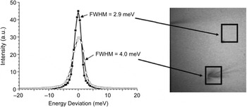
). The effect of minor defects is illustrated by comparing energy curves measured with a highly monochromatic beam. While quartz quality may not be perfect enough for 1-meV-level resolution, recent studies report good performance for energy resolutions below 10 meV for flat crystals
Reference Sutter, Baron, Miwa, Nishino, Tamasaku and Ishikawa7,Reference Kim, Shi, Casa, Qian, Huang and Gog19
and slightly above that for curved analyzers.
Reference Ketenoglu, Harder, Klementiev, Upton, Taherkhani, Spiwek, Dill, Wille and Yavaş16
Energy curves measured at two different spots on a quartz wafer. The incoming beam with 1.91 meV bandwidth is used to measure the quality of the quartz crystal. While the defect-free spot has 2.9 meV energy resolution, the slightly blemished area causes broadening in the bandwidth. Note: FWHM, full width at half maximum. Reference Sutter, Baron, Miwa, Nishino, Tamasaku and Ishikawa7

Lithium niobate
Lithium niobate (LiNbO3) is a technologically important crystal material, commonly used in both linear and nonlinear optical applications (See Table II for its crystal properties). As early as the late 1980s, it was recognized that congruent—meaning lithium-deficient—LiNbO3 crystals could be grown in near-perfect quality, making them also suitable for some x-ray optical applications. LiNbO3 has been attractive as an alternative to the more common perfect-crystal materials used in wide-ranging applications, from structural studies using the demanding x-ray standing wave technique Reference Gog, Harasimowicz, Dev and Materlik24 to spherical analyzers for RIXS. Reference Shvyd’ko, Hill, Burns, Coburn, Brajuskovic, Casa, Goetze, Gog, Khachatryan, Kim, Kodituwakku, Ramanathan, Roberts, Said, Sinn, Shu, Stoupin, Upton, Wieczorek and Yavas25
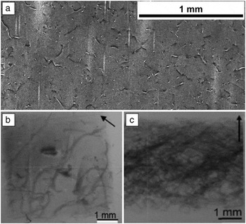
The theoretical energy resolution of lithium niobate backscattering reflections varies widely depending on the Miller indices (direction) of the reflection. Similar to quartz, and unlike high-symmetry materials with one type of atom such as silicon, lithium niobate has no monotonic trend for energy resolution as a function of energy. Reflections where the relatively high-atomic-number Nb atoms contribute strongly to scattering tend to be broader, while those where the lighter Li and O atoms contribute predominantly tend to be narrower, with nominally higher resolution (for a detailed discussion see References Reference Authier9 and Reference Shvyd’ko29). Consequently, for applications with more relaxed resolution requirements of around 100 meV or above, LiNbO3 can offer an attractive solution with high throughput (Figure 1b). For better resolution, however, crystal quality becomes an issue—the high density of threading basal plane dislocations seen in Figure 4a is a clear indication of the subpar optical quality of the crystal. This is also evident in the broadening of rocking curve measurements. These findings suggest that a significant improvement in crystal quality for x-ray applications could be attained by refining growing techniques in order to drastically reduce the density of defects.
Topography images of LiNbO3 and sapphire crystals. Dark areas correspond to regions with a high dislocation density. (a) Bragg geometry topography of a LiNbO3 wafer, clearly showing a high density of threading basal plane dislocations. (b–c) White-beam topography of two sapphire crystals grown by the Kyropoulos method: (b) grown by Asadchikov et al. (dislocation density ≈100/cm2) and (c) commercially available high-quality crystal (dislocation density >1000/cm2). Reference Asadchikov, Butashin, Buzmakov, Deryabin, Kanevsky, Prokhorov, Roshchin, Volkov, Zolotov, Jafari, Alexeev, Cecilia, Baumbach, Bessas, Danilewsky, Sergueev, Wille and Hermann34

Sapphire
Sapphire has many uses in various fields, ranging from optical windows where high durability is needed to solid-state electronics as a high-quality insulating substrate. Due to their unique structural properties, sapphire single crystals find applications in x-ray optics as well. Reference Yavaş, Ercan Alp, Sinn, Alataş, Said, Shvyd’ko, Toellner, Khachatryan, Billinge, Hasan and Sturhahn5,Reference Sergueev, Wille, Hermann, Bessas, Shvyd’ko, Zając and Rüffer12,Reference Shvyd’ko and Gerdau30–Reference Alexeev, Asadchikov, Bessas, Butashin, Deryabin, Dill, Ehnes, Herlitschke, Hermann, Jafari, Prokhorov, Roshchin, Röhlsberger, Schlage, Sergueev, Siemens and Wille32 The quality of sapphire has improved dramatically during the past few decades and the search for better methods to grow perfect crystals in large volumes is ongoing. Reference Chen, McNally, Shvyd’ko, Tuomi, Lerche, Danilewsky, Kanatharana, Lowney, O’Hare, Knuuttila, Riikonen and Rantamaki33,Reference Asadchikov, Butashin, Buzmakov, Deryabin, Kanevsky, Prokhorov, Roshchin, Volkov, Zolotov, Jafari, Alexeev, Cecilia, Baumbach, Bessas, Danilewsky, Sergueev, Wille and Hermann34 Among various techniques, the Kyropoulos method seems to be favored by the x-ray optics community (see Figure 4b–c for white-beam topographs of sapphire).
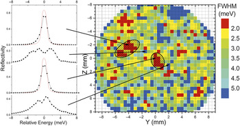
As a robust characterization method, meV topography yields a map of the surface showing contrast based on the energy bandwidth of a particular Bragg reflection ( Figure 5 ). Reference Sergueev, Wille, Hermann, Bessas, Shvyd’ko, Zając and Rüffer12 The energy curves are measured by scanning the incoming photon beam with meV precision while keeping the geometry fixed. The bandwidth, or rather its deviation from the theoretical value for a perfect crystal, is measured over the entire surface, one point at a time. Alternatively, utilizing a wide beam and a two-dimensional pixel detector, the whole surface can be swept in a few scans, where the spatial resolution is defined by the detector pixel size. Reference Jafari, Sergueev, Bessas, Klobes, Roschin, Asadchikov, Alexeev, Härtwig, Chumakov, Wille and Hermann35 A clear correlation between low-dislocation density and high-resolution areas on the crystal surface is observed. This technique is particularly useful for finding the best spot to be used as a monochromator, since the x-ray beam is usually diffracted only from a small, ∼1 mm2 portion of the crystal surface, because of the small and collimated beam of third- and fourth-generation light sources. Crystals with a (mean) dislocation density of about 100/cm2 show good spots comparable to the beam size (clear areas in right-hand image in Figure 3) while crystals with dislocation densities >1000/cm2 are not suitable for this application. Analyzers, on the other hand, require a good response over larger areas, ∼10–100 cm2, and are therefore more difficult to fabricate. The ultimate test of an analyzer is to measure the energy resolution when it is uniformly illuminated. It is important to note that even if the quality of the starting sapphire is good enough for meV resolution analyzers, the processing is not easy and may limit the manufacturing of efficient large-area x-ray optics. Reference Yavaş, Ercan Alp, Sinn, Alataş, Said, Shvyd’ko, Toellner, Khachatryan, Billinge, Hasan and Sturhahn5
Sapphire wafer meV topography. Energy curve widths are measured with a highly monochromatic x-ray beam of 24 keV, with a bandwidth of 0.65 meV. The right panel shows the map of the measured widths, while the left panel demonstrates representative energy curves corresponding to four points shown by arrows. Note: FWHM, full width at half maximum. Reference Sergueev, Wille, Hermann, Bessas, Shvyd’ko, Zając and Rüffer12

Conclusion
Nonsilicon perfect crystals have potential use as optics for high-energy resolution, and may significantly improve the quality of experimental data. Presently, the main issues lie with the materials—first, the underlying perfection of the material needs to be considered; and, second, especially for analyzers for RIXS, analyzer fabrication needs to be improved. The trigonal materials we have discussed are striking both for their enhanced number of back reflections allowing relatively large angular acceptances, and, especially for sapphire, for their potential to allow relatively efficient and simple optics at high energy. While the potential for nonsilicon crystal optics is beginning to be realized, Reference Wille, Hermann, Sergueev, Pelzer, Möchel, Claudio, Perßon, Rüffer, Said and Shvyd’ko11,Reference Sergueev, Wille, Hermann, Bessas, Shvyd’ko, Zając and Rüffer12,Reference Honnicke, Huang, Keister, Kodituwakku and Cai17,Reference Wille, Shvyd’ko, Alp, Rüter, Leupold, Sergueev, Rüffer, Barla and Sanchez31,Reference Alexeev, Asadchikov, Bessas, Butashin, Deryabin, Dill, Ehnes, Herlitschke, Hermann, Jafari, Prokhorov, Roshchin, Röhlsberger, Schlage, Sergueev, Siemens and Wille32 increased production of high-quality materials continues to be pivotal to the development of efficient high-energy-resolution optics.
Acknowledgments
T.G. acknowledges X. Huang of the Advanced Photon Source (APS) for collecting and interpreting white-beam topography images. J.P.S. acknowledges S. Stoupin (formerly APS, now Cornell), N. Pereira (Ecopulse) for useful discussions, and D. Casa (APS) for advice. This research used resources of the APS, a US Department of Energy (DOE) Office of Science User Facility operated for the DOE Office of Science by Argonne National Laboratory under Contract No. DE-AC02–06CH11357.

Hasan Yavaş is a beamline scientist at Deutsches Elektronen-Synchrotron (DESY), Germany, leading the inelastic x-ray scattering program at PETRA III. He received his PhD degree in physics from Michigan State University for work performed at Argonne National Laboratory and Princeton University. He was with the University of Illinois at Urbana-Champaign as a postdoctoral researcher before moving to DESY. Yavaş can be reached by phone at +49-40-8998-5767 or by email at hasan.yavas@desy.de.

John P. Sutter has been an optics scientist at the Diamond Light Source Ltd., UK, since 2006. He develops x-ray optics, particularly monochromators, mirrors, and lenses. He received his PhD degree in physics from Purdue University in 2000, based on research carried out at the Advanced Photon Source. This was followed by postdoctoral research at Hamburger Synchrotronstrahlungslabor (2000–2003) and at SPring-8 in Japan (2003–2006). He is a member of the American Physical Society. Sutter can be reached by phone at +44 1235 778626 or by email at john.sutter@diamond.ac.uk.

Thomas Gog is the group leader of the inelastic x-ray and nuclear resonant scattering group at the Advanced Photon Source at Argonne National Laboratory. He received his PhD degree in x-ray physics in 1990 from Purdue University, and has been a scientific staff member at various synchrotron radiation facilities. His research interests include resonant inelastic x-ray scattering and the development of ultrahigh-resolution x-ray optics for this and related techniques. Gog can be reached by phone at 630-252-0320 or by email at gog@anl.gov.

Hans-Christian Wille has been a beamline scientist at the Dynamics Beamline P01 at Deutsches Elektronen-Synchrotron, Germany, since 2010. He received his PhD degree from Hamburg University, Germany, in 2003. He completed postdoctoral research at the ID-18 beamline of the European Synchrotron Radiation Facility (ESRF), France, from 2003 to 2006. He then performed optics tests at ESRF for PETRA III at Deutsches Elektronen-Synchrotron at ID-06 until 2009. He is a member of the Deutsche Physikalische Gesellschaft. Wille can be reached by phone at +49 40 8998 5724 or by email at hans.christian.wille@desy.de.

Alfred Q.R. Baron operates an independent laboratory at RIKEN SPring-8 Center, Japan. He received his PhD degree from Stanford University. Following postdoctoral research at the European Synchrotron Radiation Facility, France, he moved to SPring-8, and was responsible for the meV-resolved inelastic x-ray scattering (IXS) program in Japan. He built two beamlines for IXS, BL35 and BL43LXU. Baron can be reached by email at baron@spring8.or.jp.