The scope for nanoscale light trapping
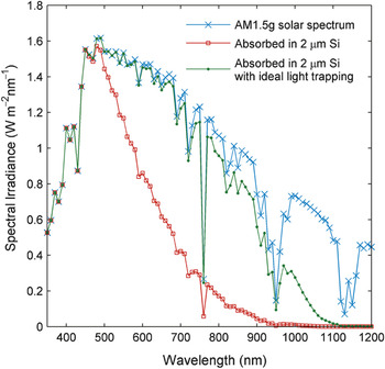
Over the past 30 years, the cost of solar modules has reduced by over a factor of 10. About half of this reduction has been due to economies of scale; the other half by progress in increasing cell efficiencies and improved fabrication methods. The major cost component for silicon modules is now the materials cost of the silicon wafers, which is 40% of the cost of the entire module. This has led to a trend toward cheaper wafers, such as multicrystalline silicon, as well as thin-film cells, such as those based on polycrystalline silicon and cadmium telluride. As solar cells become thinner, absorption losses become more important. For example, Figure 1 shows the absorption in a 2 micron thick silicon film, with and without light trapping, compared to the irradiance available in the solar spectrum.
The spectral irradiance (W m−2 nm−1) on the Earth’s surface in the standard AM1.5g solar spectrum (blue crosses). The irradiance absorbed by a 2 μm Si substrate, neglecting reflection losses (red squares), and by the same substrate with an ideal (4n 2, where n is the index of refraction) light-trapping scheme is also shown (green circles).

Until recently, the main approach to reducing these losses was to texture the surface using features a few microns in size. The behavior of such structures can be described using geometrical optics (i.e., ray tracing). Some geometrical textures are known to be highly effective, for example, upright or inverted pyramidsReference Campbell and Green1 and random textures.Reference Weber and Blakers2 However, these textures are only suitable for certain types of solar cells. Pyramids are only suitable for monocrystalline silicon, and geometrical scale surface textures, in general, are not suitable for thin-film solar cells, which have thicknesses from a few hundred nanometers to a few microns.
Many years ago, Yablonovitch and Cody showed that the limit of light trapping for a random, geometric texture was an increase in absorption for weakly absorbed light of a factor of 4n 2 (where n is the index of refraction of the material) for isotropically incident light.Reference Yablonovitch and Cody3 This is a very large enhancement, around 50 for a high refractive index material such as silicon. The reason for the enhancement is the high density of optical modes in the silicon, compared to modes in air. The derivation assumes that the light is equally distributed among all the optical modes. This means that scattering processes tend to scatter light back into the high index material, leading to the large enhancement in absorption. According to the brightness theorem (see for example Reference Reference Boyd4), it is not possible to go beyond the 4n 2 limit using geometrical optics except by narrowing the range of the angle of incidence of the light. Stuart and Hall extended the method to thin films, which only support a few waveguide modes.Reference Stuart and Hall5 They showed that because there are fewer modes available, the absorption enhancement is reduced; although with three modes, the enhancement is already within 25% of the 4n 2 limit. Thus it would seem that with thin films, the potential for light trapping is reduced, and this may indeed be the case in some circumstances. However, wavelength scale light trapping and ultrathin materials can also be used to go beyond the 4n 2 limit.
This possibility was suggested by Brendel, who gave an example of beyond 4n 2 enhancement, though in that case, it did not lead to useful electron–hole-pair generation.Reference Brendel6 It was recently shown that it is possible to go beyond 4n 2 enhancement and also generate useful absorption.Reference Yu, Raman and Fan7 These designs take advantage of the higher mode density in the near field of the active regions of the devicesReference Brendel6 or nanoscale confinement of the modesReference Yu, Raman and Fan7 (i.e., they rely on effects limited to wave optics, which do not occur in geometrical optics).
Light trapping can be advantageous for strongly absorbing thin films such as amorphous silicon and cadmium telluride, as well as weak absorbers such as crystalline silicon. For strong absorbers, the main advantage is to reduce the thickness of material required. This reduces bulk recombination, potentially allowing higher efficiencies, or alternatively allowing lower quality material to be used while still collecting photogenerated electrons and holes. Another advantage of some types of nanophotonic light trapping is that they do not lead to an increase in surface recombination that is inevitable with surface texturing. This is important because as material quality is improved, surface recombination will be the major factor limiting the efficiencies of thin-film solar cells.Reference Green8
Nanophotonic light trapping is also of particular importance to “third-generation” solar cells, which use novel structures or materials with the aim of beating the efficiencies of single junction solar cells. Examples of these solar cells are quantum well and quantum dot solar cells. Because of issues associated with fabricating these devices, such as strain in the layers, it is often only possible to grow very thin devices. Structures that can localize the light in the active layer are then crucial for achieving high performance.
Types of nanophotonic light trapping
The key feature of nanophotonic light-trapping structures is that they are similar to or smaller in size than the wavelength of light of interest for light trapping (i.e., smaller than about one micron). The materials that are used need to interact strongly with light, such as metals or semiconductors. The main approaches can be classified as plasmonic (based on metals), periodic semiconductor or dielectric structures (gratings and photonic crystals), and randomly structured semiconductor surfaces. In addition, there is increasing research into nanowires for solar cells, which show strong photonic effects. This section describes the mechanisms and state of the art for each type of light trapping. A more detailed description of these topics can be found in several chapters of Reference Reference Tsakalakos9.
Plasmonic light trapping
A plasmon is a collective oscillation of electrons in a metal. Plasmonic light trapping can involve either metal nanoparticles or continuous metal films. We will look at the case of particles first.
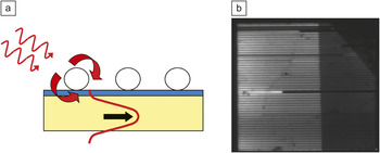
Particles have a resonant frequency at which incident light will strongly excite the collective oscillation of electrons. This leads to either strong absorption or strong scattering of light. For moderately sized nanoparticles (larger than 100 nm in diameter) made of a low loss metal such as silver, scattering is by far the dominant effect. If the particle is within a few tens of nanometers of a high index semiconductor, the scattered light will couple strongly into the semiconductor, because there are many more optical modes available in the semiconductor than in air (Figure 2a). The particle needs to be within a few tens of nanometers because the scattered field around the particle decays evanescently (i.e., exponentially) away from the particle. This is sometimes described as a coupling of the “near-field” of the particle to the semiconductor. Near-field coupling can be pictured using the analogy of earphones for sound. When you are far away from earphones, there is no significant transfer of sound to your ear. However, when the earphones are in your ear (i.e., you are in the near-field of the sound source), there is strong transfer of sound wave energy.
(a) Light (red waves) incident on a metal nanoparticle excites a plasmon resonance, which then couples to a waveguide mode in an underlying semiconductor. (b) Electroluminescence from a silicon light-emitting diode. The left half of the device is covered with metal nanoparticles. The whole device is 1 mm × 1 mm. Reprinted with permission from Reference Reference Pillai, Catchpole, Trupke, Zhang, Zhao and Green11. ©2006, American Institute of Physics.

Metal nanoparticles have been used to achieve an enhancement in photocurrent of 33% for thin silicon solar cells.Reference Pillai, Catchpole, Trupke and Green10 These structures can also be used to improve light-emitting diodes,Reference Pillai, Catchpole, Trupke, Zhang, Zhao and Green11 since by the generalized Kirchoff’s law, a good absorber is a good emitter.Reference Würfel12Figure 2b illustrates the enhancement in emission that can be achieved using silver nanoparticles on the surface of a silicon light-emitting diode.
Plasmonic light trapping using particles on the surface is suitable for very thin solar cells because it involves no structuring of the active layer. It also avoids the increase in surface recombination that occurs with a textured surface. A passivating layer can be placed between the metal particles and the active layer to avoid the high level recombination that would occur with a metal/semiconductor interface. In addition, the application of the particles does not interfere with normal cell processing, since the particles are deposited at or close to the final stage in the fabrication process.
Since the initial reports demonstrating the promise of plasmonic light trapping,Reference Pillai, Catchpole, Trupke and Green10, Reference Schaadt, Feng and Yu13–Reference Derkacs, Lim, Matheu, Mar and Yu15 a great deal has been learned about how to optimize plasmonic light-trapping structures. It has been shown that placing particles on the front of solar cells leads to constructive interference between transmitted and scattered light, and hence enhancement in absorption at wavelengths above the plasmon resonance. However, it also leads to destructive interference and hence reduced absorption at wavelengths shorter than the plasmon resonance.Reference Lim, Mar, Matheu, Derkacs and Yu16 This can be minimized by blueshifting the plasmon resonance or avoided entirely by placing the particles at the rear of the cell.Reference Beck, Catchpole and Polman17 It has also been shown that not only the coupling but also how strongly the light is scattered changes depending on where the particles are placed, due to changes in the electric field driving the oscillation at the position of the particle. In addition, greatly increased scattering can be achieved for particles directly on the rear of a cell, and the achievable cell performance can be better than with diffuse reflectors.Reference Beck, Mokkapati, Polman and Catchpole18, Reference Ouyang, Pillai, Beck, Kunz, Varlamov, Catchpole, Campbell and Green19 Substantial enhancements have been achieved with both random and periodic arrays of particles.Reference Lim, Derkacs and Yu20 It has also been demonstrated that particle arrays can enhance the efficiency of third-generation solar cells based on III–V quantum dot materials,Reference McPheeters, Hill, Lim, Derkacs, Ting and Yu21 and significant enhancement is also predicted for ultrathin cadmium telluride solar cells.Reference Qilin22
Another form of plasmonic light trapping involves coupling of light to propagating surface plasmon polaritons on a metal film, followed by absorption in a nearby semiconductor. A surface plasmon polariton is a wave propagating at the interface of a metal and a dielectric, confined by its high in-plane momentum. Bumps or grooves on the metal surface can be used to couple incident light either to the plasmonic interface mode or to photonic waveguide modes propagating inside the semiconductor. Strong enhancement can be achieved with this approach by using structured back reflectors. For relatively weak absorbers, such as silicon, it is more advantageous to couple to the photonic modes because this avoids the losses in the plasmonic modes.Reference Ferry, Sweatlock, Pacifici and Atwater23 Indeed, for both metal films and metal particles, it is important to consider losses in the metal as well as absorption in the active layer.Reference Franken, Stolk, Li, v.d. Werf, Rath and Schropp24, Reference Akimov, Koh, Sian and Ren25
Absorption enhancement in semiconductors can also be achieved by making use of the enhanced near-fields around resonant metallic structures.Reference Kirkengen, Bergli and Galperin26 Since the near-field is only a few tens of nanometers in extent, it is necessary to use strong absorbers with this approach. It has been shown that this, together with scattering effects, could lead to substantial absorption enhancement in amorphous silicon solar cells.Reference Pala, White, Barnard, Liu and Brongersma27 Furthermore, absorption of around 40% could be achieved in ultrathin active layers approximately10 nm thick.Reference Hägglund and Kasemo28 This opens up possibilities for a new class of ultrathin photovoltaic devices, provided that a suitable electrical design could be incorporated. Near-field enhancement would be expected to be especially beneficial for relatively low refractive index active layers such as organics, which (because of the 4n 2 relation) benefit less than high index materials from scattering-based absorption enhancement. More detailed overviews of plasmonic light trapping can be found in References Reference Tsakalakos9, Reference Atwater and Polman29, and Reference Catchpole and Polman30.
Gratings and photonic crystals
Periodic dielectric structures can also be used to enhance absorption in solar cells. The main types of periodic structures are 1D multilayer (Bragg) stacks, 2D gratings, and 3D photonic crystals.Reference Joannopoulos, Meade and Winn31 These structures are illustrated in Figure 3. Aside from their intrinsic potential for improving light trapping, periodic structures are important because their relatively well-developed theory and simulation methods assist in gaining a fundamental understanding and allow for a more direct comparison between theory and experiment than with other structures.
Schematic illustration of nanophotonic structures used for light trapping: (a) 1D (Bragg) stacks used as back reflectors; (b) 2D gratings used for light trapping; (c) 3D photonic crystals, which are highly effective as omnidirectional reflectors; and (d) nanowires, which trap light by a waveguiding effect.

The main mechanism involved in light trapping with periodic structures is interference between different modes propagating in the structure. In that sense, they are an extension of the simple quarter-wave anti-reflection coating, which uses interference of the incident and reflected waves to give low reflectance over a reasonably broad wavelength range. Anti-reflection coatings are universally used in solar cells. In Bragg stacks, rectangular gratings and 3D photonic crystals optical modes interfere either constructively or destructively, leading to either high transmission through the structure or high reflectance. Bragg stacks are usually engineered to create high reflectance over a particular wavelength range. They can be highly effective as a low loss reflector and are used extensively in lasers. However, their wavelength and angular sensitivity are not ideal for solar cells. Three-dimensional photonic crystals can also be designed to give very high reflectance, but 3D structures have the advantage of a much reduced angular sensitivity. In general, 3D structures are much more challenging to fabricate, but for designs that are not very sensitive to disorder or defects, simple self-assembly techniques can be used.Reference Xia, Gates and Li32 Three-dimensional photonic crystals also have the potential to increase absorption by other mechanisms, for example by light localization due to multiple resonant modes.Reference Mihi and Miguez33
Two-dimensional gratings have diffraction orders given by the well-known grating equation

where θ is the angle of propagation in each medium, m is the grating order (an integer), λ is the wavelength of light, and L is the period of the grating. For rectangular 2D gratings, the amount of light directed to each grating order can be understood using a simple picture of interference of modes within the grating, and such gratings can effectively direct light toward high diffracted orders that are trapped within the solar cell.Reference Catchpole and Green34 Overall, many types of grating have been shown to lead to very effective light trapping.Reference Heine and Morf35–Reference Zhou and Biswas39 Blazed gratings, which are asymmetric structures designed to direct light into a particular diffraction order, have been theoretically shown to increase the optical effective thickness of a thin cell by a factor of five.Reference Heine and Morf35 One-dimensional photonic crystals have been combined with rectangular gratings in a design that acts as a bandpass filter as well as a light trapping device for application to tandem cells.Reference Mutitu, Shi, Chen, Creazzo, Barnett, Honsberg and Prather37 Dual period rectangular gratings have also been proposed, with calculated enhancements of a factor of three over the spectral range 920–1040 nm.Reference Lee, Huang, Chang and Wu38 Furthermore, although the 4n 2 limit can only be exceeded for a broad wavelength and angular range in limited cases, gratings have been shown theoretically to substantially exceed this limit over restricted wavelength ranges.Reference Zhou and Biswas39 Experimentally, by combining a rear grating with a textured photonic crystal back reflector, an external quantum efficiency enhancement of 135 times at a wavelength of 1200 nm has been reported.Reference Zeng, Yi, Hong, Liu, Feng, Duan, Kimerling and Alamariu36 It should be noted that comparison of large enhancement results with theoretical predictions would require very accurate measurements of the initial absorptance or quantum efficiency.
A special case of grating structures is that of the sub-wavelength gratings. An example of this in nature is the moth eye. Such gratings have periods less than the wavelength of light, and only the zeroth grating order exists (i.e., only m = 0 is a solution of the grating equation). Such gratings can be viewed as an effective medium since they act to refract light with an effective refractive index intermediate between the refractive indices of the materials that compose the grating. For non-rectangular gratings, the refractive index changes gradually across the grating layer. Because they act as an effective medium, these structures do not provide light trapping, but they can act as very effective anti-reflection layers.Reference Boden and Bagnall40, Reference Zhu, Yu, Burkhard, Hsu, Connor, Xu, Wang, McGehee, Fan and Cui41
For practical application, the electrical performance of the solar cell in the presence of a grating or photonic crystal structure also needs be considered. If a grating is fabricated in the active layer of the solar cells, it tends to lead to increased surface recombination. Additionally, if the active layer is deposited on a substrate with a grating structure, steep features can make subsequent deposition of high-quality material difficult.
Nanowires
Solar cells based on nanowires have been proposed and developed recently. Nanowire solar cells consist of arrays of long semiconductor cylinders, usually arranged vertically, but not necessarily periodically. An example structure is shown in Figure 3d. Nanowire structures are strongly photonic, and it has been shown that nanowires can lead to excellent light trapping.Reference Kelzenberg, Boettcher, Petykiewicz, Turner-Evans, Putnam, Warren, Spurgeon, Briggs, Lewis and Atwater42–Reference Muskens, Rivas, Algra, Bakkers and Lagendijk44 Kelzenberg et al. have shown that for nanowire arrays with a packing fraction around 5%, absorption similar to Lambertian (4n 2) absorption for an equivalent thickness silicon layer can be achieved.Reference Kelzenberg, Boettcher, Petykiewicz, Turner-Evans, Putnam, Warren, Spurgeon, Briggs, Lewis and Atwater42 This very high absorptance for such a low packing fraction suggests that their properties may be more due to the individual nanowires than to a collective, grating-like effect. Path length enhancements of 73 have been demonstrated for perpendicular incidence of light waves for silicon nanowire arrays on silicon substrates.Reference Garnett and Yang43 (This is a very impressive result, but note that it does not in itself exceed the 4n 2 limit since that applies to isotropic incidence.)
The p-n junction in these solar cells is often formed radially in these devices, which has the advantage of separating the functions of charge carrier collection and optical absorption.Reference Kayes, Atwater and Lewis45 The growth of very good material qualityReference Putnam, Turner-Evans, Kelzenberg, Boettcher, Lewis and Atwater46 and other advantages have also been demonstrated, including the ability to detach the nanowire structure from the growth substrate.Reference Plass, Filler, Spurgeon, Kayes, Maldonado, Brunschwig, Atwater and Lewis47 Device modeling has shown that efficiencies of 20% may be possible with CdS/CdTe nanowire solar cells,Reference Kapadia, Fan and Javey48 and promising experimental cell efficiencies have been reported for silicon,Reference Tian, Zheng, Kempa, Fang, Yu, Yu, Huang and Lieber49, Reference Sivakov, Andrä, Gawlik, Berger, Plentz, Falk and Christiansen50 III-nitrides,Reference Dong, Tian, Kempa and Lieber51 and for Si/GaN heterojunctions.Reference Tang, Chen, Song, Lee, Cong, Cheng, Zhang, Bello and Lee52 The main challenge associated with the radial design is the need for very low recombination in the junction region,Reference Kayes, Atwater and Lewis45, Reference Stocks, Cuevas and Blakers53, Reference Catchpole, Mokkapati and Beck54 which may lead to this design being most suitable for certain material systems such as CdS/CdTe.Reference Kapadia, Fan and Javey48
Random scattering
Random scattering surfaces are an important type of nanophotonic light-trapping structures because they are very simple to fabricate, and they allow a wide angular and wavelength range to be trapped. In addition, effective light trapping can be achieved with minimal parasitic absorption.Reference Battaglia, Soderstrom, Escarre, Haug, Domine, Cuony, Boccard, Bugnon, Denizot, Despeisse, Feltrin and Ballif55, Reference Rockstuhl, Fahr, Bittkau, Beckers, Carius, Haug, Söderström, Ballif and Lederer56 Because of the complexity of the interaction of these surfaces with light, there is limited theoretical guidance for the design of these surfaces. However, it has been shown that it would be advantageous to direct light outside the escape cone (i.e., at high angles so that it will be totally internally reflected),Reference Fahr, Rockstuhl and Lederer57 and criteria for the depth of local features can be derived.Reference Rockstuhl, Fahr, Lederer, Bittkau, Beckers and Carius58 As with grating structures, increased surface area can lead to increased surface recombination, and steep features can lead to reduced material quality if deposited on a textured surface. If the design includes a conformal metal reflector, it also will be important to minimize coupling to the metal because structured metals can be strongly absorbing.Reference Franken, Stolk, Li, v.d. Werf, Rath and Schropp24, Reference Bonod and Popov59
Fabrication and characterization
One of the most important reasons for the rapidly increasing interest in nanophotonic light trapping is the advances that have been made in fabrication, numerical simulation, and characterization at the nanoscale. While it has been possible to fabricate random nanoscale features by etching for many years, until recently, it has not been possible to design, fabricate, and measure controlled features. Nanophotonic applications are not as demanding as some other nanoscale technologies, but still require control on at least the scale of 100 nm. An important distinguishing requirement for photovoltaic applications is that in order to be sufficiently low cost, throughput has to be extremely rapid, and an industrially applied technology ultimately will be required to cover square kilometers.
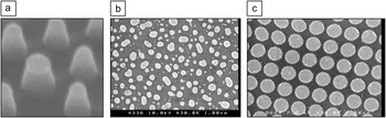
Some of the techniques that have been used to make nanophotonic structures are etching or evaporation through self-assembled colloidal masks,Reference Velev and Gupta60–Reference Inns, Campbell and Catchpole62 evaporation and annealing,Reference Gupta, Dyer and Weimer63 and nanoimprinting.Reference Verschuuren and Sprang64, Reference Guo65 Examples of these structures are illustrated in Figure 4. Other techniques include deposition and etching of thin polycrystalline layersReference Müller, Rech, Springer and Vanecek66 and maskless reactive ion etching.Reference Ruby, Zaidi, Narayanan, Damiani and Rohatgi67
Scanning electron micrographs of (a) a silicon grating fabricated by colloidal self-assembly followed by reactive ion etching. The spacing between the cones is 400 nm. Reproduced with permission from Reference Reference Inns, Campbell and Catchpole62. ©2007, Hindawi Publishing Corporation. (b) Metal nanoparticle structures fabricated by evaporation and annealing. (c) Metal nanoparticles formed by nanoimprinting followed by metal lift-off. The metal nanoparticles have a diameter of 400 nm. Parts b and c are on the same scale.

In colloidal self-assembly, an array of nanospheres on a surface is produced by spin coating or dip coating. The nanospheres are usually silica or polystyrene, which can be produced using chemical methods with a high degree of uniformity. Colloidal self-assembly processes have the advantage of being very cheap and simple, but suffer from a lack of control. Either very sparse arrays or multiple layers of particles tend to be produced. This can be an advantage for some applications, such as 3D photonic crystals, but is less suitable for 2D patterning of a surface.
In evaporation and annealing, a thin layer of metal (usually around 15 nm) is deposited by thermal evaporation or a similar method. This is then annealed at around 200°C, and the film breaks up into islands by surface tension. Evaporation and annealing is a cheap and simple technique that can be used to produce dense arrays of metallic particles for plasmonic applications. It is possible to achieve a moderate degree of control with this technique. However, a range of sizes are always produced, and little control over particle coverage is possible.
Textured polycrystalline transparent conductive oxides are widely used in the fabrication of thin-film cells.Reference Müller, Rech, Springer and Vanecek66 The usual process is deposition followed by wet etching, which creates a texture because of the different etching rates of the various crystal planes. The structure is advantageous because the texture is introduced at the same time as the transparent top contact of the device. The active layer is then deposited conformally on the textured surface. The disadvantage of this method is that it can be difficult to get a structure that scatters sufficiently, and the electronic quality of the active layer can also be compromised.
One of the most promising methods of forming nanophotonic structures is nanoimprinting. Nanoimprinting uses either a hard or soft reusable stamp to directly texture a substrate, with a resolution of 50 nm, and a very high degree of control over the surface texture. Large areas can be imprinted, and roll-to-roll nanoimprinting is also possible. Nanoimprinting has been used to fabricate back reflector and superstrate gratings as well as plasmonic particle arrays for thin-film solar cells.Reference Battaglia, Soderstrom, Escarre, Haug, Domine, Cuony, Boccard, Bugnon, Denizot, Despeisse, Feltrin and Ballif55, Reference Ferry, Verschuuren, Li, Schropp, Atwater and Polman68, Reference Wang, Mokkapati, Beck, Ouyang, Varlamov and Catchpole69
In order to realize highly effective light-trapping structures, nanoscale simulation and characterization techniques are also important. Simulation of periodic structures is now straightforward with techniques such as finite difference time domain and rigorous coupled wave analysis; commercial software is available to do this. Simulation of non-periodic structures is still very computationally expensive; however, even using a computer cluster and 3D simulations are currently limited to around a micron in size.
For periodic structures, large-area characterization techniques can be used. However, for non-periodic structures, much more information can be gained by using local measurements. For example, scanning near-field optical microscope (SNOM) measurements have been used to show regions of enhanced field and strong scattering on random surface textures.Reference Rockstuhl, Lederer, Bittkau and Carius70 SNOM measurements also have been used to identify high-performing regions using photocurrent mapping.Reference Sundararajan, Grady, Mirin and Halas71 This is a new area, and we can expect important new information from these types of measurements.
Summary and outlook
Nanophotonic light trapping provides the potential to improve the current generation of solar cells as well as to create high-efficiency cells using novel materials and cell designs. The rapid development in the field of nanophotonic light trapping has led to a range of new possibilities in solar cell development. Examples of these are the opportunities in the design of light-trapping structures for particular applications, such as ultrathin cells made from strong absorbers using near-field effects or for wavelength selective light-trapping design for tandem cells. Successful new structures will integrate strong light trapping, low reflectance, low parasitic loss, and compatibility with fast semiconductor deposition processes. Successful structures will also have excellent electrical properties, which offer the possibility of interesting synergies for new solar cell designs. In the next few years, we can expect to see further rapid development in this area, along with integration with other developments in the field of photovoltaics.
Acknowledgments
This work was supported by the Australian Research Council. A.B. is grateful to the Austrian Science Fund (FWF)—project J 2979.