I. INTRODUCTION
Polymer solar cells (PSCs) have gained considerable attention as a promising renewable energy source due to their potential for cost-effective energy generation.Reference Kippelen and Bredas1–Reference Cheun, Fuentes-Hernandez, Zhou, Potscavage, Kim, Shim, Dindar and Kippelen3 In recent years, as a result of tremendous efforts focusing on the synthesis of new conjugated polymers and the design of novel device architectures, PSCs with a power conversion efficiency higher than 8% have been achieved.Reference Dou, You, Yang, Chen, He, Murase, Moriarty, Emery, Li and Yang4, Reference Zhou, Yang and You5 In spite of progress in the performance of PSCs, further improvement in device stability is still needed for PSCs to compete with other emerging photovoltaic technologies.Reference Jorgensen, Norrman and Krebs6
Conventionally, low work function (WF) metals such as Ca/Al and LiF/Al have been used as electron-selective electrodes, while high-WF conducting materials such as poly(3,4-ethylenedioxythiophene):poly(styrene sulfonate) (PEDOT:PSS)-modified indium tin oxide (ITO) have been utilized as hole-selective electrodes.Reference Waldauf, Morana, Denk, Schilinsky, Coakley, Choulis and Brabec7 However, the facile oxidation of these low-WF metals in air causes a severe lifetime reduction of PSCs without encapsulation.Reference Li, Wen, Lee, Guo, Huang, Lin and Hsu8 To circumvent this problem, PSCs with a so-called inverted geometry have been introduced and developed. In an inverted geometry, PSCs do not require low-WF metals as top electrode. Instead, high-WF metals with better environmental stability such as silver (Ag) or gold (Au) are placed at the top of the device to collect holes.Reference Kuwabara, Sugiyama, Kuzuba, Yamaguchi and Takahashi9 A common route to realize inverted PSCs has been to reduce the WF of ITO to a value that is low enough to be used as an electrode-selective layer. This reduction of WF is commonly achieved by coating ITO with thin layer of metal oxides such as aluminum oxide (Al2O3),Reference Zhou, Cheun, Potscavage, Fuentes-Hernandez, Kim and Kippelen2 zinc oxide (ZnO),Reference Cheun, Fuentes-Hernandez, Zhou, Potscavage, Kim, Shim, Dindar and Kippelen3 and titanium oxide (TiOx),Reference Waldauf, Morana, Denk, Schilinsky, Coakley, Choulis and Brabec7–Reference Steim, Choulis, Schilinsky and Brabec12 or an alkali metal salt, cesium carbonate (Cs2CO3).Reference Liao, Chen, Xu, Li and Yang13 Coating of these materials is generally done by evaporation under high vacuum or by spin coating, when solution-based precursors of these materials are available. When processed from solution, some of these materials such as TiOx require post-fabrication thermal treatments at high temperatures.Reference Li, Wen, Lee, Guo, Huang, Lin and Hsu8 However, the use of deposition processes requiring high vacuum or thermal treatment at relatively high temperatures is less desirable for its use on high throughput methods or for the fabrication of PSCs on flexible substrates. Work function modification methods that allow low temperature processing and are compatible with high throughput methods are therefore required.
Among a number of metal oxides, titanium oxide layers (TiOx or TiO2) have been used in a variety of applications such as a photoelectrode in dye-sensitized solar cells, as an electron-selective layer in PSCs, and as a photocatalyst.Reference Kim, Lee, Gomez, Kim and Loo10–Reference Steim, Choulis, Schilinsky and Brabec12, Reference Dai, Weng, Sui, Shi, Huang, Chen, Pan, Fang, Hu, Kong and Wang14, Reference Karthick, Prabakar, Subramania, Hong, Jang and Kim15 In the context of PSCs, many different groups have reported various techniques to synthesize TiOx or TiO2 layers. For example, sol-gel methods (including a conversion of the titanium oxide precursor by hydrolysis), atomic layer deposition (ALD), and chemical bath deposition (CBD) have been used to achieve an electrode with good electron selectivity in PSCs.Reference Kim, Lee, Gomez, Kim and Loo10, Reference Schmidt, Zilberberg, Schmale, Flugge, Riedl and Kowalsky11 In addition, a nonhydrolytic sol-gel method with cesium (Cs)-doped TiO2 layer was demonstrated as electron transport layer in organic solar cells. However, some of these methods still need a sintering process at a high temperature, processing under vacuum, or an additional step to remove agents that hinder nanoparticle agglomeration.Reference Park, Li, Kumar, Li and Yang16
More recently, a mixture of ZnO nanoparticles and poly(N-vinylpyrrolidone) (PVP), referred to as ZnO:PVP nanocomposite, has been introduced as electron transport layer in PSCs.Reference Small, Chen, Subbiah, Amb, Tsang, Lai, Reynolds and So17 Unlike pristine ZnO nanoparticles, the ZnO:PVP nanocomposite film provides better film uniformity as well as a lower density of defects in the film.Reference Small, Chen, Subbiah, Amb, Tsang, Lai, Reynolds and So17 The nanocomposite is synthesized by coordinating the polymer dispersant PVP, which has an amphiphilic nature due to the highly polar amide and nonpolar methylene groups, onto the hydrophilic nanoparticles. This approach has also been applied for dispersion of many metal oxides, including TiO2.Reference Hassouna, Therias, Mailhot and Gardette18−Reference Kamiya, Fukuda, Suzuki, Tsukada, Kakui and Naito23
In our study, we introduce an electron-selective layer processed from an aqueous solution. This layer comprises titanium dioxide (TiO2) nanoparticles dispersed in polyvinylpyrrolidone (PVP) (TiO2:PVP). The changes in WF when this mixture was used to coat ITO were determined by using a Kelvin probe in air, and the surface morphology was examined by atomic force microscope (AFM). Inverted PSCs with a poly (3-hexylthiophene) (P3HT): [6,6]-phenyl-C61-butyric acid methyl ester (PC60BM) active layer and a TiO2:PVP-coated ITO electrode, used as electron-selective layer, were fabricated. Two reference cells in which either ITO only or ITO/TiO2 served as electron-collecting electrodes also were tested. The inverted PSC with the TiO2:PVP electron-selective layer showed a power conversion efficiency of 3.0 ± 0.2%, an open circuit voltage of 592 ± 1 mV, a short circuit current density of 8.3 ± 0.5 mA/cm2, and a fill factor of 0.61 ± 0.01 after exposing the solar cells for 25 min under a 100 mW/cm2 AM 1.5G solar illumination.
II. EXPERIMENTAL
A. Device fabrication
Inverted PSCs with the TiO2:PVP-coated ITO electrodes were fabricated by blending the donor P3HT (4002 E, Rieke Metals Inc., Lincoln, NE) with the acceptor PC60BM (Nano-C). P3HT:PC60BM solutions were made in chlorobenzene (CB, Sigma Aldrich, St. Louis, MO) with a weight ratio of 1:0.7 and a total concentration of 34 mg/mL. ITO-coated glass (Colorado Concept Coatings LLC, Loveland, CO) with a sheet resistivity of 15 Ω/sq. was used as a substrate. Substrates were cleaned in an ultrasonic bath of detergent (Liqui-Nox®, SPI Supplies/Structure Probe, Inc., West Chester, PA) in water, rinsed with distilled water, and then washed in sequential ultrasonic baths of distilled water, acetone, and isopropanol. Nitrogen was used to dry the substrates after each of the last three washes. A 300 nm-thick layer of SiOx was deposited though a shadow mask on the ITO substrate by e-beam deposition (AXXIS, Kurt J. Lesker, Clairton, PA), for patterning the electron-collecting electrode. Next, the substrates were ultrasonicated in isopropanol for 10 min, and blown dry with nitrogen. Titanium dioxide nanopowder (Sigma Aldrich, Average nanoparticle size 21 nm) and PVP (Sigma Aldrich) were dispersed in distilled water with a total concentration of 0.14 wt% (TiO2:0.07 wt% and PVP: 0.07 wt%). The solution was ultrasonicated for 30 min, and then centrifuged at a rotation speed of 3000 rpm for 5 min (Eppendorf Centrifuges 5804 R, Eppendorf AG, Hamburg, Germany). A small volume, taken from the top of the centrifuged solution, was spin-coated onto ITO at 3000 rpm for 1 min. A 30 nm-thick TiO2:PVP film was then annealed at 80 °C for 10 min in ambient air. After loading into a nitrogen-filled glove box, a 180 nm-thick active layer was deposited on the substrates by spin coating for 1 min at 1000 rpm and annealed at 160 °C for 10 min. The solution of the active layer materials was filtered through a 0.2 μm-pore polytetrafluoroethylene (PTFE) filter prior to spin coating. An 80 nm-thick PEDOT:PSS layer, (CLEVIOS CPP D105, H.C. Starck, München, Germany) was then spin-coated on top of the active layer at 2000 rpm for 45 s and annealed at 120 °C for 10 min inside the glove box. The substrates were loaded into a vacuum thermal evaporation system (SPECTROS, Kurt J. Lesker) connected to the glove box, and 150 nm of Ag was deposited through a shadow mask, to define the active area, at a rate of 1–2 Å/s and a base pressure of 2 × 10⁻⁷ Torr. The active area was around 0.1 cm2 and determined accurately under a microscope for each individual device. The completed devices were transferred in a sealed container to another nitrogen-filled glove box for electrical measurements. Before electrical measurements, all devices were exposed to light from an AM1.5 Global (G) solar simulator (Oriel, 91160, Newport Corporation, Irvine, CA) with an irradiance I L = 100 mW/cm2, through the substrate, for 25 min. Current-voltage characteristics (J-V) were measured, inside a nitrogen-filled glove box, using a source meter (2400, Keithley, Cleveland, OH) controlled by a LabVIEW program. Solar cells under illumination were tested using the AM1.5 Global (G) solar simulator previously described.
B. Characterization of the TiO2:PVP layer
Atomic force microscopy (AFM) studies of independent films of TiO2 and TiO2:PVP on ITO-coated glass substrates were carried out using a MultiMode AFM (Dimension 3100, Veeco, Santa Barbara, CA) equipped with a NanoScope III controller. Studies of the work function (WF) values of TiO2 on ITO-coated glass substrates, TiO2:PVP on ITO-coated glass substrates, and bare ITO-coated glass substrates (reference) were conducted by using a Kelvin probe (Besocke Delta Phi, Jülich, Germany) in ambient air. X-ray photoelectron spectroscopy (XPS: K-Alpha, Thermo Scientific, Waltham, MA) was also conducted on TiO2:PVP on ITO-coated glass substrates, and bare ITO-coated glass substrates (reference). The core level of Ti and the core level of nitrogen atoms in PVP were used to study the surface composition of these samples. XPS was implemented with an Al K-alpha monochromatic source of photons having energy of 1486.6 eV and a 300 μm spot size.
III. RESULTS AND DISCUSSIONS
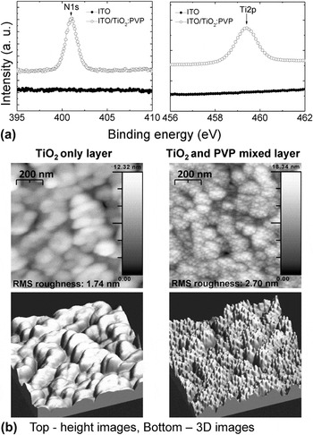
For confirming the presence of each surface component in TiO2:PVP (1:1, by weight) films deposited on ITO, XPS measurements were conducted. Samples with specific ratios TiO2 and PVP were selected for study based on the performance of PSC as will be shown below. Figure 1(a) compares XPS data from bare glass/ITO and glass/ITO/TiO2:PVP substrates. The peaks around 400 eV (N, 1S), and 460 eV (Ti,2P), indicate the presence of PVP and TiO2. To examine the surface morphology, TiO2 and TiO2:PVP films were studied by AFM. Figure 1(b) shows AFM topographic images of the TiO2 and TiO2:PVP-coated ITO/glass substrates. These images reveal a root-mean-square surface roughness of 1.74 nm for TiO2 films and 2.70 nm for TiO2:PVP films. However, a noticeable difference was found in morphology. Before adding the PVP dispersant, the TiO2 nanoparticles appeared to be aggregated. However, well-dispersed, individual TiO2 nanoparticles were observed with the PVP dispersant. Otherwise, TiO2 nanoparticles are highly aggregated even after 30 min of ultrasonication, as shown in the TiO2 film without PVP modification.
(a) XPS spectrum of the N1s and Ti2p core level for ITO and ITO/TiO2:PVP surfaces. (b) AFM images (top: height images, bottom: 3D images) of TiO2 (left) and TiO2:PVP (right) on glass/ITO substrates

The WFs of the TiO2-coated ITO substrates was found to be 4.47 ± 0.02 eV (averaged over 3 points) and of 4.33 ± 0.02 eV (averaged over 3 points) for TiO2:PVP-coated ITO substrates. For comparison, the WF of ITO is 4.65 ± 0.02 eV (averaged over 3 points). A highly oriented pyrolytic graphite (HOPG) sample with a WF of 4.5 eV was used as the reference. Although only modest reductions of the WF are observed, the WF value of the TiO2:PVP modified ITO-coated substrates is similar to that of ZnO-coated ITO electrodes which have previously been used for the realization of inverted PSCs.
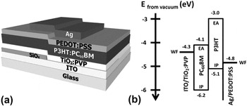
To investigate the performance of solar cells with TiO2:PVP-coated ITO electrodes, we fabricated inverted PSCs with a layered structure of: glass/ITO/TiO2:PVP/P3HT:PC60BM/
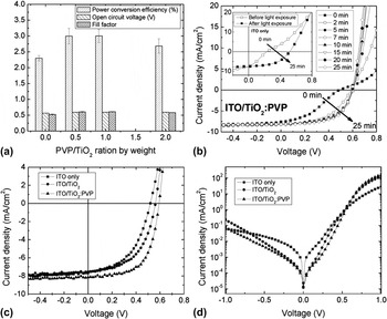
PEDOT:PSS/Ag, shown in Fig. 2. To examine the effect of the ratio of the PVP to TiO2 (by weight) on the PSC device performance, four PSC devices with ITO electrode coatings having different PVP/TiO2 ratios of 0, 0.5:1, 1:1, and 2:1 were fabricated. Figure 3(a) shows the device performance parameters, power conversion efficiency (PCE), open circuit voltage (V OC), and fill factor (FF) as a function of the PVP to TiO2 nanoparticle ratio. The presence of PVP is found to improve the device performance. Although no major differences are found between devices having PVP/TiO2 ratios of 0.5:1 and 1:1, a clear decrease in performance is observed for devices with a 2:1 ratio. This decrease in performance may be attributed to the excessive concentration of PVP, which is known to be an insulator.Reference Small, Chen, Subbiah, Amb, Tsang, Lai, Reynolds and So17
(a) Device structure of an inverted P3HT:PC60BM solar cell with ITO/TiO2:PVP for an electron-collecting electrode. (b) Energy level diagram of the components of the solar cell device (WF stands for work function, EA for electron affinity and IP for ionization potential).

In the following part, we will discuss in detail the properties of PSCs with PVP:TiO2 (1:1 wt%) layers. Figure 3(b) shows the J-V characteristics of pristine and light-exposed devices with the ITO/TiO2:PVP electron selective electrodes. Pristine devices exhibited an S-shaped kink causing a low FF of 0.37, a small V OC of 490 mV, and a PCE of 1.39%. These pristine devices were subjected to the continuous illumination, inside a N2-filled glove box, from the simulated AM 1.5G illumination source. After 10 min of irradiation, the S-shape disappeared and remained unchanged after up to 25 min of exposure. After exposure, the PSCs with the ITO/TiO2:PVP electron selective electrode displayed an V OC of 592 ± 1 mV, a short circuit current density (J SC) of 8.3 ± 0.5 mA/cm2, a FF of 0.61 ± 0.01 and a PCE of 3.0 ± 0.2%. The PCEs of these devices are comparable to P3HT:PC60BM-based inverted PSCs, where titania (TiO2 or TiOx)-coated ITO has been used as an electron-collecting electrode and when the active layer was processed by doctor blading (PCE = 3.1%)Reference Waldauf, Morana, Denk, Schilinsky, Coakley, Choulis and Brabec7, by CBD (PCE = 3.21%)Reference Kuwabara, Sugiyama, Kuzuba, Yamaguchi and Takahashi9 and by spin coating (PCE = 2.4%).Reference Kim, Lee, Gomez, Kim and Loo10
(a) PCE, V OC, and FF of inverted P3HT:PC60BM solar cells with ITO/TiO2:PVP electrodes having various weight ratios between PVP and TiO2. (b) J-V characteristics of solar cells with ITO/TiO2:PVP electrodes under illumination, as a function of light exposure time. Inset: J-V characteristics of solar cells with ITO only electrodes under illumination, before and after light exposure. (c) Representative J-V characteristics under illumination for inverted P3HT:PC60BM solar cells with ITO, ITO/TiO2, and ITO/TiO2:PVP electrodes. (d) Representative semi-log J-V characteristics in dark for inverted P3HT:PC60BM solar cells with ITO, ITO/TiO2, and ITO/TiO2:PVP electrodes.

The appearance of an S-shape kink in the J-V characteristics of PSCs has been related to poor charge selectivity of an electrode. This lack of selectivity generally arises from an increased contact recombination that in this case would lead to a slow rate of electron collection. Upon illumination, a reduction of the WF of ITO is expected.Reference Olivier, Servant, Vergnolle, Mosca and Garry24, Reference Wang, Lu, Hsu, Lee, Hong, Perng, Horng and Meng25 This reduction would lead to an improved electron selectivity of the electrode.
For confirming the reduction of WF upon illumination, ITO and TiO2:PVP-coated ITO substrates were subjected to 25 min of light exposure under the solar simulator through the glass side (as the PSC devices). After the light exposure, the WF of ITO was 4.45 ± 0.02 eV (averaged over 3 points); a significant reduction compared with its initial value prior to light exposure (4.65 ± 0.02 eV). Similarly the WFs of the TiO2:PVP samples decreased from 4.33 ± 0.02 eV to 3.99 ± 0.02 eV (averaged over 3 points) after light exposure. The values of the WF obtained with the Kelvin probe appear to be low enough to provide good electron selectivity, given the electron affinity (EA) of PC60BM (4.1 eV).Reference Cheun, Fuentes-Hernandez, Zhou, Potscavage, Kim, Shim, Dindar and Kippelen3 It is expected however that even though the TiO2:PVP layer appears to be homogeneous on the microscopic scale, it will not likely be fully conformal, and thus regions of uncoated ITO would be exposed. The nonconformal coverage will result in a spatial distribution of nanometer size domains with high (bare ITO) and low (TiO2:PVP-covered ITO) work function across the surface of the electrode. Hence, the areas with higher work function will offer poor electron-selectivity and consequently will yield J-V curves with S-shape characteristics. Upon UV exposure, the electron-selectivity of these areas improve as the work function of ITO decreases, leading to a much better the electron selectivity of the entire electrode. This hypothesis is supported by the fact that when ITO alone is used as electron-collecting electrode, the reduction of its work function upon illumination in solar cell devices leads to the disappearance of the S-shape kink from its J-V characteristics, as shown in the inset of Fig. 3(b).
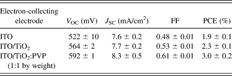
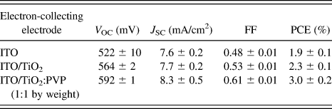
For comparing the performance of the TiO2/PVP-coated ITO electrode with coatings of pure TiO2 nanoparticles and with bare ITO, two other inverted PSCs with a structure of glass/ITO/TiO2/P3HT:PC60BM/PEDOT:PSS/Ag and a structure of glass/ITO/P3HT:PC60BM/PEDOT:PSS/Ag were made by following identical processing conditions as previously described, with the exception of the electron-selective layers. For making a fair comparison of the above devices with those having a TiO2/PVP-coated ITO electrode, the devices were exposed for 25 min under the solar simulator before measuring the electrical characteristics of these PSCs. As observed in the TiO2/PVP-coated ITO electrodes, the WF of the TiO2-coated ITO electrode decreased from 4.47 ± 0.02 eV to 4.26 ± 0.02 eV after light exposure. Figures 3(c) and 3(d) show a comparison of the J-V characteristics of the three inverted PSCs, after being exposed to light for 25 min, under illumination (c) and in dark (d). Table I summarizes the photovoltaic performances, averaged over five devices, of all the PSCs cells evaluated. The PSCs with ITO as electron-collecting electrodes exhibited a V OC of 522 ± 10 mV, a J SC of 7.6 ± 0.2 mA/cm2, a FF of 0.48 ± 0.01 and a PCE of 1.9 ± 0.1% while the PSCs with ITO/TiO2 as electron-collecting electrodes exhibited a V OC of 564 ± 2 mV, a J SC of 7.7 ± 0.2 mA/cm2, a FF of 0.53 ± 0.01 and a PCE of 2.3 ± 0.1%.
Summary of the averagedFootnote a device performance of inverted P3HT:PC60BM (1:0.7 by weight) solar cells with ITO, ITO/TiO2, and ITO/TiO2:PVP (1:1 by weight) electron-collecting layer. 25 min light exposure was performed on ITO, ITO/TiO2, and ITO/TiO2:PVP devices before measurement.
a Average was calculated over five devices.
For PSCs with an ITO electron-collecting electrode, in the absence of band-bending effects, even after the light exposure a relatively large energy level mismatch of 0.35 eV can be expected between the WF of the ITO (4.45 eV) and the electron affinity (EA) of PC60BM. While these PSCs work, the small value of the FF (0.48) and V OC (522 mV) indicates that the electron-selectivity of these electrodesReference Wagenpfahl, Rauh, Binder, Deibel and Dyakonov26 is poor in comparison to PSCs that use a TiO2/PVP-coated ITO electrode, having a FF of 0.61 and V OC (592 mV). In the case of the PSCs with the TiO2 layer, there is a slight improvement in all the parameters of the device performance compared with PSC devices with bare ITO electrodes, leading to a 20% higher PCE than devices with bare ITO electrodes, but the performance is inferior to that of PSCs with an TiO2/PVP-coated ITO electrode. We have found that in addition to assisting in the dispersion of TiO2 nanoparticles in an aqueous solution, PVP also provides an additional contribution to the WF reduction observed in TiO2/PVP-coated ITO electrodes. A detailed study of the role of PVP as a surface modifier that reduces the WF of ITO will be presented elsewhere.
IV. CONCLUSIONS
In this report, we investigated the morphological and electrical properties of a new electron-selective electrode, TiO2:PVP-coated ITO. As a dispersant, the PVP was able to coordinate onto and disperse TiO2 nanoparticles uniformly in films on top of ITO. The TiO2:PVP-coated ITO electrode was shown to provide good electron-selectivity in inverted PSCs. After being exposed to light from a solar simulator for 10 min, devices with TiO2:PVP-coated ITO electrodes showed around 1.8 times larger PCE values than devices with TiO2-coated ITO electrodes. Light exposure was shown to lead to reductions of the WF of ITO, TiO2-coated ITO and TiO2:PVP-coated ITO electrodes. The need for light exposure prior to optimum device operation may be related to the nonconformal coverage in the nanometer scale of the spin-coated layers used to coat the ITO surface. In addition to assisting the dispersion of the TiO2 nanoparticles, the addition of PVP was found to lead to even larger reductions of the WF in TiO2:PVP-coated ITO electrodes compared with TiO2-coated ITO electrode, and consequently to inverted PSCs with improved performance.
ACKNOWLEDGMENTS
This work was funded in part through the Center for Interface Science: Solar Electric Materials, an Energy Frontier Research Center funded by the U.S. Department of Energy, Office of Science, Office of Basic Energy Sciences under Award No. DE-SC0001084 (H.C, Y.Z., J.S., B.K.), by the STC Program of the National Science Foundation under Agreement No. DMR-0120967 (C.F., D.K.H.), and by the Office of Naval Research (Grant No. N00014-11-1-0462) (A.D., Y.K, J.W.P.). Part of this work was performed at the Microelectronics Research Center at Georgia Institute of Technology, a member of the National Nanotechnology Infrastructure Network, which is supported by NSF (Grant No. ECS- 03-35765).