I. INTRODUCTION
Since the beginning of their development in the early 2000s, RF MEMS (Micro Electro Mechanical Systems) have always suffered from a lack of reliability, hampering their mass production, and commercialization. These limitations are due to the complex underlying physics of failure dominated by strong multiphysics and multiple scale phenomena, made fuzzier by the shortcoming in technology stability, which needs yet to meet industrial standards. As far as technical bottle-neck issues are concerned, one of the major failure mechanism identified in the past was the dielectric charging, which induces a drift of pull-in and pull-out voltages, and quickly leads to permanent stiction in open or closed state. However recent publications have clearly showed that this phenomenon is no more the main failure cause for ohmic micro-contact switches, since it can be avoided by means of design tricks or control voltages tuning approaches [Reference Mardivirin, Bouyge, Pothier, Crunteanu-Stanescu and Blondy1]. Consequently, another failure mechanism becomes the predominant one, i.e. the degradation of the resistive micro-contact properties throughout the switch's lifetime.
As for dielectric charging, intense research activity is mandatory to study the root causes of this failure, and to derive solutions to overcome it. This is made difficult by the small sizes at stake in these devices, and by the multiphysical aspect of the micro-contacts. Indeed, mechanical, thermal, electrical, and even chemical aspects have to be taken into account to elaborate an accurate behavioral model. In particular, the contact pressure and the corresponding temperature have to be determined precisely, knowing that these two parameters are interdependent. In order to do so, the model needs to be completed by sets of data that include the electrical and the thermo-mechanical properties of the thin-film metallizations used to realize the contact. Hence, a new set-up was developed for the characterization of contact materials used in micro-switches. In previous works the study of the Au/Au, Ru/Ru, and Au/Ru contact resistance, comparing the stability with respect to an increased level of current has been already presented [Reference Broue2–Reference Broue4]. The present paper intends to recall these previous results to extend and focus on critical aspects, such as contact asperity, joule-effect-induced heating, and finally contact adhesion. These studies are systematically carried out with different levels of current and for several pairs of different contact materials.
The work presented in this paper aims at demonstrating the enhanced stability of bimetallic contacts compared to mono-metallic ones. A comparison of five contact pairs is presented, clearly highlighting a lower sensitivity of the bimetallic ones to temperature effects.
II. BACKGROUND THEORY
The micro-contact physically differs from the macro-contact due to the influence of surface roughness and the smaller contact force available in micro switches. Only high points on each surface come in contact, and the effective contact area, named asperities or a-spots, is largely smaller than the apparent one. The way the electrons are transported through electrical connections (ballistic, quasi-ballistic, or ohmic transport) needs to be determined to evaluate the resistance of contact. A detailed presentation of the different conduction modes (ohmic, ballistic, and mixed) and of the mechanical aspects (plastic and elastic deformation) can be found in [Reference Broue2]. In the model used here the conduction mode is considered to be ohmic and the deformation mainly plastic. This assumption can be used to describe the deformation of the asperities during the first actuations, known as “burn-in” phase.
A) Conduction mode
For a single circular spot of contact, “ohmic contact” means that the contact radius a, is at least one order of magnitude higher than the mean free path l e of the electrons in the material. In this case the Ohm's law can be applied at each point in the contact. The measured resistance is then dominated by a diffuse scattering mechanism, and is given by the Holm resistance formula. This electrical resistance is directly linked to the constriction of current lines between the contacts. It causes a local increase of the current density and tends to increase the electrical potential drop between the two sides of the asperity. The expression of this constriction resistance is
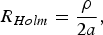
where ρ is the resistivity of the contact material. It is necessary to keep in mind that generally the current flows by multiple asperities. The easiest approach consists in considering that the whole conductance 1/R eff is the sum of the conductances 1/R n of the multiple contact spots with varying sizes (no interaction between the spots):
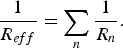
This expression is a first approximation. More complex models can be used to find an accurate approximation [Reference Holm5].
B) Deformation mode
When the two contact surfaces collide with each other, the asperities of each contact could have three deformation modes: elastic, elastic–plastic, and plastic, depending on the level of stress applied to the materials. During the first contact establishment between the two surfaces, the stress applied on the high points of the asperities is generally higher than the yield stress of the contact material. This is due to a necessary roughness adaptation of the surfaces. Thus the deformation of the contact asperities is considered to be predominantly plastic. The contact area and the contact load can be linked to the radius of the contact spot a using Abbott and Firestone's plastic contact model [Reference Holm5]:
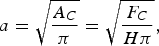
where A C is the contact area, F C the contact force, and H the Meyer hardness of the softer material. This leads the stress to reduce toward the yield point after several actuations, where the behavior becomes closer to a domain of perfect-elastic or elastic–plastic transition. Thus, only perfect-plastic behavior will be first considered, by applying Abbott and Firestone's plastic contact model.
C) Contact temperature model
Heating of the contact spots is extremely localized when the current flows through the contact: the device level remains at room temperature but softening or melting temperatures can be reached on the asperities [Reference Jensen, Chow, Huang, Saitou, Volakis and Kurabayashi6]. The highest contact spot temperature T C has been expressed by Kohlrauch as a function of the contact voltage V c for an ohmic contact [Reference Holm5]:
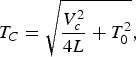
where L = 2.45 × 10⁻⁸ W Ω/K2 is the Lorentz constant and T 0 the ambient temperature. Equation (5) is obtained from the Wiedemann–Franz law for a conductor heated by the current produced by the voltage V C between two arbitrary isotherms with the temperature T 0: the assumption is made that the thermal and electric currents obey similar laws thus with symmetric contacts the generated heat flows in the same path as the electric current. The resistivity is also dependant on the temperature.
D) Performances and reliability of micro contacts
Performances of electrical contacts in MEMS switches are strongly linked with the materials used. Their mechanical and electrical properties will govern the evolution of the contact resistance when the load is applied, as well as its sensitivity to the main failure mechanisms: Three types of root causes can be highlighted: the mechanical (cold welding, wear, and strain hardening), electrical (arcing, hot welding, and annealing), and chemical ones (formation of insulating films at the extreme surface), all inducing modifications of the topological, mechanical, and electrical properties of the contact. The best compromise between mechanical and electrical performances has to be found to reach reliable operations. The material must have good electrical conductivity to avoid losses, high melting point to handle power, appropriate hardness to avoid stiction, and chemical inertness to avoid oxidation [Reference Kwon7]. This information can be partly found in the literature, but it does not replace a direct quantitative characterization of the MUT, as it is done by means of the setup presented in next subsection.
III. METHODOLOGY
A) Description of the experimental set-up
Advanced characterization of the contact properties requires high control of the load applied to the contact, of the displacement of the moving part, and of the electrical properties of this contact. These conditions can be reached using a nanoindenter coupled with a high-resolution source meter. The spherical diamond tip acts as a mechanical actuator, which applies a punctual load on the free-standing electrode mimicking the switch action at the contact interface. Previous works described the set-up and showed the relevance of such an approach to simulate a distributed actuation pressure [Reference Kwon7] while additional information can be found in [Reference Broue2, Reference Broue3].
B) Test vehicle description
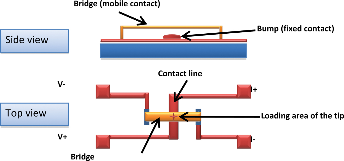
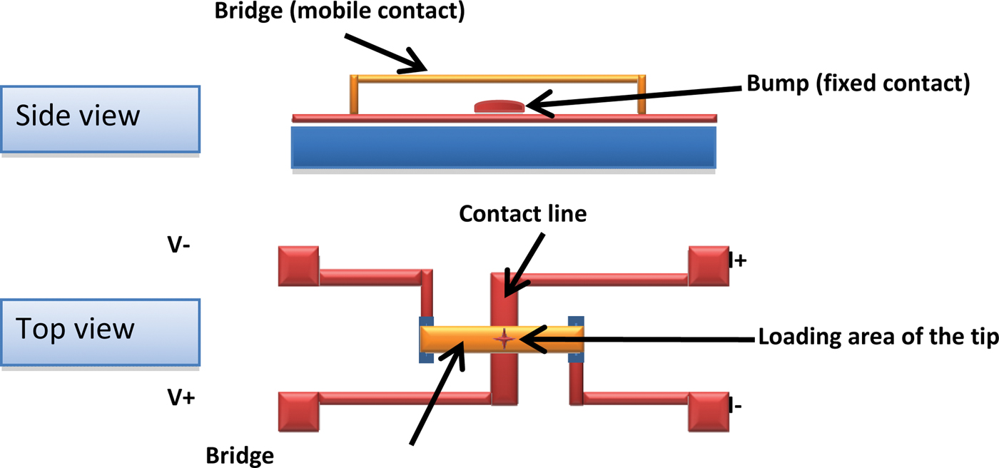
Specific test vehicles have been designed to allow an efficient extraction of characteristic curves and make possible the comparison between different contact shapes or materials. As illustrated in Fig. 1, the microfabricated devices are composed of a bridge suspended over a contact line. Thanks to a true four-point system and the specific design, only the contact resistance is measured, being the resistance of the remaining structure, lines and bridge patterned on the substrate automatically removed. This method for measuring contact resistance is the same as the one used in the crossed rod design of Holm [Reference Holm5]. A 3 µm × 3 µm bump is processed underneath the bridge.
Schematic of the test structures.
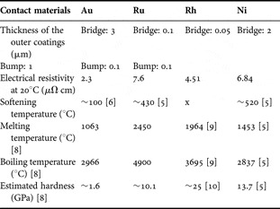
Four contact materials are tested (cf. Table 1): first gold, which is the most popular material for electrical contact because of its high bulk conductivity, its high oxidation resistance, its low propensity to form alien surface films [Reference Patton and Zabinski11], and its compatibility with MEMS fabrication methods. However, gold is a soft material subject to large surface modifications while switching cycles occur. Furthermore, gold is prone to contact wear and stiction, which affect the contact performance. This is the reason why new contact metals such as Ru, Rh, and Ni, have been introduced. These are much harder than pure Au or any Au alloy. They may provide better resistance stability in spite of a higher bulk resistivity [Reference Ke, Miao and Oberhammer12]. On the other hand, ruthenium and rhodium are typical frictional polymer-forming metals, they tend to adsorb organic vapor from air and form a contaminating film [Reference McGruer, Adams, Chen, Guo and Du13]. Nevertheless, the introduction of these contact metal candidates, endowed with higher melting point, gives the opportunity to investigate their behavior under large current levels.
List of properties of switch contact metals.

Five kinds of test structures with different contact metals are used for this study: Au/Au, Ru/Ru, Au/Ru, Rh/Rh, and Au/Ni. They have been successfully fabricated at LETI (Au, Ru, Ni) and NTB (Rh contact), and stored in dry N2 to slow down any environmental contamination of the contact surfaces. In spite of that, gradual contamination accumulation still occurred due to the device transfer between the different laboratories. The thicknesses of each contact material are synthetized in Table 1.
IV. EXPERIMENTAL RESULTS
A) Contact force versus contact resistance
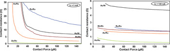
First of all, the contact resistance evolution with increasing contact force and current levels are studied. The results are presented in Fig. 2. When the contact is established between two metallic electrodes, the effective contact area is very low. Only the higher points of the electrodes are in contact. The contact area is then very low and the contact resistance is high and unstable. At a certain minimum force, depending on the material under investigation, a significant reduction of the resistance occurs as considerable plastic deformation takes place, causing rupture of undesired films at the contact interface. At higher forces, the contact remains stable and the resistance decreases slightly with further increasing of the force until a saturated regime is reached [Reference Schimkat14].
Contact resistance versus contact force as a function of the current flowing through the contact for Au/Ru, Au/Au, Ru/Ru, Rh/Rh, and Au/Ni contacts at 1 and 100 mA.

Figure 2 shows the contact resistance for Au/Ru, Au/Au, Ru/Ru, Rh/Rh, and Au/Ni contacts as a function of the measured contact force with a contact current of 1 and 100 mA. Concerning mono-metallic contacts, one can see that the resistivity of the materials governs the level of resistance obtained both at 1 and 100 mA.
The Au/Ru bimetallic contact is relatively stable at maximum contact load. The behavior of the Au/Ru contact seems nearer to a very soft material rather than being in between a soft and a hard material. This confirms that in an asymmetric contact made of a soft and a hard material is the former to dictate the overall behavior. Our assumption is that the asperities of the softer material are much more deformed by a hard material surface. The results on Au/Ni contact are quite surprising because of the high level of the contact resistance, which is consistently higher than the expected one for 1–100 mA. It is suspected that the Ni part of the contact collected a large layer of contaminants on the contact surface because of a long period of hazardous storage.
Special efforts have to be made to well understand these first results. In general, the results on Au/Ru provided an attractive trade-off between low contact resistance and handling of relatively high power as will be shown in the next section.
B) Contact heating focus
To further examine the heating effect on contact resistance, the study is focused on the contact temperature when the maximum contact load is reached at 150 µN by gradually loading and unloading the bridge with an increased current level at each cycle. The methodology consists in measuring the contact voltage while applying the current through the asperities. The contact temperature is then calculated by means of the contact voltage measured across the contact (5).
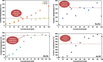
The published softening temperature for gold contact is ~100°C, corresponding to a contact voltage of 70–80 mV for contact near room temperature [Reference Holm5]. For Au/Au contact, the current is increased until reaching the softening temperature, around 40 mA (Fig. 3). Then, the contact resistance continues to decrease keeping the contact temperature roughly constant. The contact temperature increases with a constant slope from 1 to 40 mA. The potential drop across the contact remains almost constant between 65 and 75 mV (from 80 to 120°C). The same behavior is partially observed for other symmetrical contact Ru/Ru. The published softening temperature for ruthenium contact is ~430°C, corresponding to a contact voltage of 200 mV and contact near room temperature [Reference Umemoto15]. As pointed out previously, when the softening temperature is reached, the contact temperature does not depend strongly on contact current at high current levels. Beyond this value, the contact temperature is unstable even though it seems to oscillate around this softening temperature. To our knowledge, the softening temperature of rhodium is still unknown, and has not been reported yet in the literature. This pronounced leveling of the potential occurs in the same manner than for Au/Au and Ru/Ru contacts. This result suggests that the softening temperature of rhodium is around 360°C.
Contact temperature versus the contact current for Au/Au, Au/Ru, Ru/Ru, Rh/Rh, and Au/Ni contacts at 150 µN.

On the other hand, the behavior for the bimetallic contacts Au/Ni and Au/Ru defers from the two others. As shown in Fig. 3, the contact temperature increases with the current level without reaching a maximum. And the leveling of the potentials across the Au/Ni contact is observed, but for contact temperatures largely higher than the nickel or the gold softening temperature. In asymmetrical contacts, the temperature distribution within the contact constriction is not comparable to the one in symmetrical contacts: as the conductivity of both materials is different, thermoelectric effects appear.
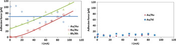
C) Determination of adhesion forces
The set-up used provides a measurement of the exceeding force required to reopen the contact with a continuously increasing tensile force. The force sensor of the nanoindenter measures the adhesion during the discontinuing of the mechanical and electrical contact. Moreover, the evolution in the pull-off force while increasing the current is tracked in order to show variations on the adhesion versus the contact temperature (Fig. 4). These tests are done in a quasi-cold switching mode (I = 1 µA and V c = 0.05 mV) and with a relative humidity below 5% to guarantee low moisture content conditions.
Pull-off force versus contact current for each contact material – bimetallic contacts exhibit low adhesion forces.

Results on Au/Au contact show that the contact begins to adhere with a really low current. The increase of the current level does not affect the contact adhesion. These results can be explained by the low contact resistance (<0.2 Ω) for the Au/Au contacts generated by a large contact area at 150 µN. This yields to an increase of the metallic bond and leads to a higher adhesion between the contact surfaces. For the Ru/Ru and Rh/Rh cases, the behavior differs from the gold one. Adhesion is continuously increasing from low to medium power.
Au/Ru and Au/Ni contacts show low adherence without high evolution of the pull-off force. The evolution of the pull-off force with increasing current is really different for bimetallic contacts as this kind of contact prevents the adherence between the contact parts. More extensive exploration of the adherence conditions have to be done to explain why the adhesion seems to become smaller for the bimetallic contacts.
V. DISCUSSION
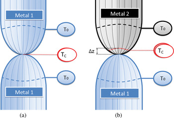
The previous section pointed out the dissimilar behavior of symmetrical and asymmetrical contact materials. For the symmetrical contacts, the potential across the contacts cannot really exceed the softening voltages at these current levels. On the contrary, the asymmetrical contacts may withstand voltages beyond the softening level of the contact materials. Figure 5(a) provides a schematic view of the symmetric case (same material, Metal 1).
Temperature distribution (a) in a symmetric constriction (b) in the constriction of a contact between two metals Metal 1 and Metal 2 with different conductivities and hardness.

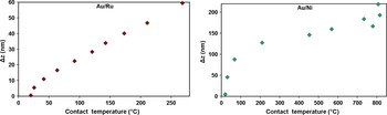
The assumption that the electrical and thermal currents flow in the same paths, is always supported by the Wiedemann–Franz law [Reference Holm5]. T 0 is the bulk temperature in the both members of the contact. The highest temperature T C is localized at the extreme contact interface across which no heat flows for a monometallic contact. The temperature distribution is symmetric around the hottest contact spot precisely localized at the intersection between both parts of the contact. Figure 5(b) illustrates the temperature distribution at the contact constriction between two different metals (Metal 1 and Metal 2) with different conductivities (ρ metal2 > ρ metal1) and mechanical hardness (H metal2 > H metal1) [Reference Holm5]. The temperature distribution around the hottest area at the contact interface has changed because of the different nature of both contact parts. Thus there is a change in the average distance of the thermoelectric heat flow. The maximum temperature T C is located within the less conductive material at a distance Δz from the physical interface [Reference Holm5]. A simple model predicts the location of the maximum temperature in a bimetallic contact [Reference Slade16]:

where ΔV is the potential drop between the physical interface and the plane of maximum temperature, ρ 1,m and ρ 2,m are the electrical resistivity of material 1 and 2 at the maximum temperature T C. Figure 6 depicts the location of the maximum temperature in the less conductive member of the bimetallic contact. The maximum temperature is always located within the hardest materials (Δz MAX = 60 nm for ruthenium and Δz MAX = 220 nm for nickel). Consequently, it has no influence on the contact asperities, and on the voltage and resistance measured. In addition, this explains that the highest adhesion occurs between identical metals, whereas bimetallic combinations exhibit weaker adhesion [Reference Stachowiak, Batchelor and Stachowiak17]. The threshold temperature observed for Au/Ni contact is probably a softening of the contact surfaces generated by the heat produced within the nickel member, and dissipated by conduction to the contact interface.
Location of the plane of maximum temperature in Au/Ru and Au/Ni contacts as a function of the maximum temperature.

VI. CONCLUSION
This test facility enables new characterization tests of MEMS ohmic contacts under realistic conditions. An emphasis was placed on the role of the low- to medium-power range leading to contact heating. First, the electro-mechanical responses of different contact configurations have been investigated. Au/Au and Au/Ru contacts have good performances and enhanced power-handling capability because of the electro-mechanical properties of the contact configuration. As a general rule, bimetallic contact should be able to handle relatively larger power, thanks to the electro thermal properties of this specific contact configuration. In addition, it has been demonstrated that bimetallic contacts reduce adherence during the unloading phase alleviating or reducing the common failure mechanism of stuck contacts. On this regard, Au/Ru contact seems to be a promising candidate for MEMS switches.
ACKNOWLEDGEMENTS
This work was supported by the ANR (Agence Nationale de la Recherche) and EURIMUS, respectively, in the framework of the FAME and SMARTIS projects.
 Adrien Broué received his French engineering degree, “Ingénieur de l'Institut National des Sciences Appliquées de Toulouse” in 2007. Since December 2007, he has been working as a PhD student on failure phenomena of ohmic contacts on MEMS switches. His PhD is a collaboration between NovaMEMS, which provides unique services in technology analysis and qualification of microtechnologies, and the Laboratoire d'Analyse et d'Architecture des Systemes – Centre National de la Recherche Scientifique of Toulouse. Most of his experiments are led at the laboratory AQ/LE in the CNES, Toulouse.
 Jeremie Dhennin received his master degree in micro- and nanophysics from the University of Paul Sabatier in Toulouse, France, in 2005. He joined NOVA MEMS as a research engineer working on multiphysical characterization and modeling of MEMS switch failure mechanisms. His current research activities focus on RF MEMS switches reliability, especially dealing with microcontact issues. He is now in charge of the project management for part of the NOVA MEMS team.
Nourredine Benjemaa IEEE Senior Member received the Doctorat es-sciences in physics from the University of Rennes I, France, in 1985. He is currently a professor of physics and electronics at the University of Rennes I where he directs group research on electrical contacts of the institute of Physics. His researches cover the physics and degradation encountered in electrical contacts. This research has been mainly concerned with low and medium electrical levels and focused on arc parameters and contact resistance. His work has been published in more than 100 papers mainly in ICEC, Holm, NARMS, IEEE journals and applied currently in the telecommunication and automobile fields. For theses scientific and technical achievement he received R Holm awards IEEE paper prices.
 Peter Heeb received his Dipl. Ing. FH degree from the University of Applied Sciences Buchs, Switzerland, in 2005. The M.Sc. degree he received from the University of Applied Sciences Vorarlberg, Austria, in 2009. Since 2005 he works as a R&D engineer at the Institute for Micro- and Nanotechnology of the University of Applied Sciences Buchs. At the Institute of Micro- and Nanotechnology he is specialized in the fields of micro (electro-)mechanical system development, hermetic packaging and mechanical testing.
 Dr. Fabio Coccetti received the Laurea (MS) degree in Electrical Engineering from the University of Perugia, Perugia, Italy and the PhD title in High Frequency Engineering at the Lehrstuhl für Hochfrequenztechnik at the Technische Universität München (TUM) in Munich Germany, in 1999 and 2004 respectively. In 2000 he has been seven months as visiting scientist at the Radiation Lab at University of Michigan USA. Since September 2004 he is working as research scientist at the Laboratoire d'Analyse et d'Architectures des Systèmes at the Centre National de la Recherche Scientifique (LAAS-CNRS) in Toulouse, France. During this period he has worked on numerous research projects going from the theoretical and experimental investigation of power handling in RF-MEMS to design modelling and experimental validation of RF Micro and Nanosystems. During 2004 – 2007 he has been the coordinator of the European Network of Excellence on RF-MEMS and RF Microsystems (AMICOM NoE). Since September 2008 he has been hired as project manager by the company Novamems, hosted as research scientist in LAAS.
His research interests include numerical techniques optimization, multiphysics (concurrent electrical and thermo-mechanical), design and modelling of reconfigurable circuits for microwave and millimetre applications and more recently he has joined as principal investigator a number of national and European projects focusing reliability assessment of RF-MEMS components. Dr. Coccetti is member of the IEEE society, since January 2009 vice-chair of the MTT-S TC-25 on RF-Nanotechnology and cofounder of the Topical Group on RF-MEMS within the European Microwave Association (EUMA)
 Dr. Patrick Pons received the PhD degree in electronics from Toulouse University (France), in 1990. Since 1991 he has been a researcher in the National Scientific Research Center - Laboratory of Analysis and Architecture of Systems in Toulouse. His research interests are focused inmicrotechnology and microsensors. In 1995, he started studying microtechnology for microwave applications. Now he manages the development of this technology for high frequency microsystems, and also develops pressure sensors for specific applications. In 2005 he started research in a new field coupling sensors and RF for the development of passive wireless sensors.
 Pr. Robert Plana obtained its PhD in 1993 at LAAS-CNRS and Paul Sabatier University on noise modeling and characterization of advanced microwave devices (HEMT, PHEMT, and HBT) that includes reliability. He has been a professor at Paul Sabatier University and Institut Universitaire de France, since 2000, and he has started a research team at LAAS-CNRS in the field of micro- and nanosystems for rf and millimeterwave communications. Its main interests are in the technology, design, modeling, testing, characterization, and reliability of RF MEMS for low noise and high-power millimetre wave applications, and the development of the MEMS IC concept for smart microsystem. He has built a network of excellence in Europe in this field, “AMICOM,” regrouping 25 research groups. He has authored and coauthored more than 300 international journals and conferences. In 2004, he was appointed as Deputy Director of the Information and Communication Department at the CNRS Headquarter. Since November 2009, he has been appointed as head of the Department of Physics, Mathematics, Nanosciences, and Nanotechnology, Information, and Communication Technology at the Ministry of Research, in charge of defining the French strategy for research and innovation.