Introduction
It is now well established that the mechanical properties of metals and alloys, such as strength, ductility, or toughness, result almost exclusively from the ability of dislocations to multiply and move through the crystalline lattice. Various approaches have been taken to tailor microstructures in order to improve these properties.Reference Vetterick, Leff, Marshall, Baldwin, Misra, Hattar and Taheri1–Reference Ovid’ko, Valiev and Zhu5 Advanced chemistries have historically been the most popular approach to tune dislocation mobility; this is being explored currently for the design of high-entropy alloys.Reference Miracle and Senkov4 Multiplying grain boundaries (GBs), ultimately resulting in nanocrystalline (nc) materials,Reference Ovid’ko, Valiev and Zhu5 has also become a classical way to increase the yield strength of a material, but often at the expense of ductility. Combining both approaches can circumvent some of the drawbacks,Reference Hu, Shi, Sauvage, Sha and Lu6 which indicates that GBReference Barr, Thomas, Hart, Harlow, Anber and Taheri2 and twinReference Leff and Taheri7 engineering are probably key to fine-tuning the properties of future alloys.
In situ mechanical testing has become an essential technique to investigate the impact of composition and microstructure on material properties, in particular because one can observe the mechanisms at play.Reference Messerschmidt8–Reference Yu, Legros and Minor10 Its versatility is further enhanced by recent quantitative capabilities, such as automated crystal orientation mapping (ACOM), or piezo-/microload cells-equipped transmission electron microscopy (TEM) holders and scanning electron microscopy (SEM) stages.Reference Legros9–Reference Kang, Merrill and Wheeler13 Visualization of the deformation of submicron volumes, a key feature of these recent developments, helps to close the gap between experiments and calculations. So does faster mechanical testing,Reference Ramachandramoorthy, Milan, Lin, Trolier-McKinstry, Corigliano and Espinosa14 which may also help unveil deformation mechanisms via the activation volume analysisReference Ramachandramoorthy, Gao, Bernal and Espinosa15 of variable strain-rate experiments. Among all of the mechanisms studied in situ, those involving GBs are particularly difficult to decipher, despite their major implications for macroscopic properties. In particular, dislocation–GB interactionsReference Malyar, Micha, Dehm and Kirchlechner16–Reference Chassagne, Legros and Rodney18 and GB-based plasticity where boundaries act as strain carriers,Reference Legros, Gianola and Hemker19–Reference Zhu, Cao, Wang, Deng, Li, Zhang and Mao21 are critical processes that need both high-resolution imaging and statistical analysis.
Understanding strain accommodation at GBs
Initially developed for crystal orientation mapping, quantitative diffraction methods may also be used to calculate geometrically necessary dislocation (GND) densities during deformation of metals by relating the curl of the orientation field to Nye’s dislocation density tensor.Reference Leff and Taheri7,Reference Leff, Weinberger and Taheri22–Reference Nye, Leff, Barr and Taheri24 This approach was originally pioneered in the electron backscatter diffraction (EBSD) community, but has since been shown to be applicable to orientation mapping in the TEM as well.
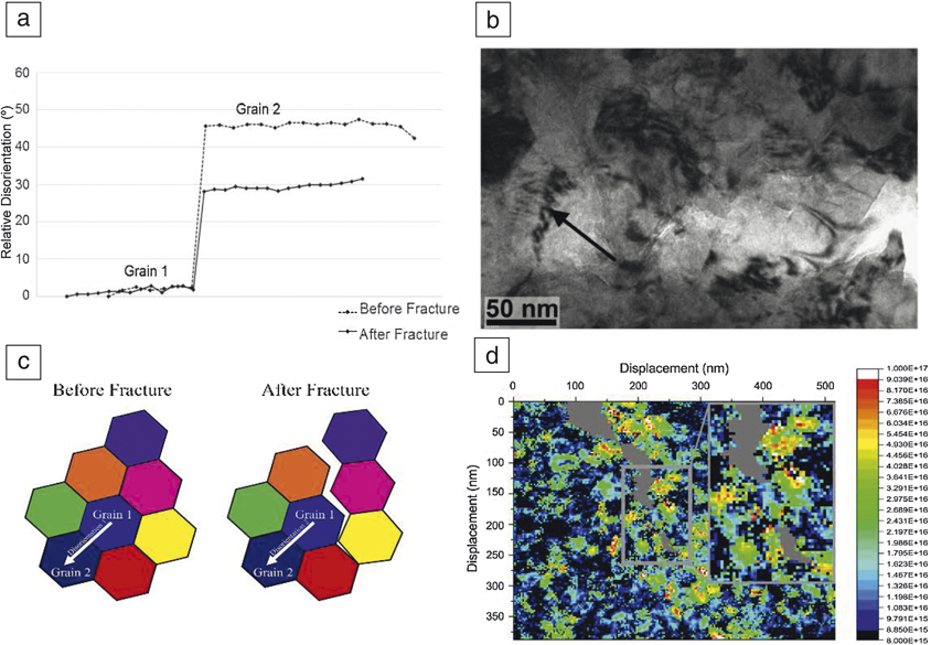
Recently, the deformation of nc-Fe films was studied through coupled in situ TEM tensile testing and quantitative dislocation density analysis (Figure 1). Orientation maps were acquired intermittently during in situ TEM tensile testing using automated crystal orientation mapping (ACOM–a NanoMEGAS analysis system). The orientation measurements were used to calculate GND density values, a lower-bound estimate of the dislocation density required to accommodate a measured lattice curvature.Reference Leff, Weinberger and Taheri22 ACOM data can be fed directly into equations to calculate the Nye tensor, as described in Reference Reference Leff, Weinberger and Taheri22.
(a) Quantitative measurement of grain rotation and disorientation, in a nc-Fe thin film undergoing mechanical deformation, (b) shown via in situ transmission electron microscopy imaging and (c) schematically. (d) Spatial mapping of dislocation density measured during the deformation process. Reprinted with permission from Reference Reference Vetterick, Leff, Marshall, Baldwin, Misra, Hattar and Taheri1. © 2018 Elsevier.

The use of electron microscopy methods to study dislocation content, in general, is dependent on various microscope parameters.Reference Leff and Taheri7,Reference Leff, Weinberger and Taheri22–Reference Ruggles and Fullwood27 For TEM specifically, these include spot size, step size, beam precession angle, and detection efficiency. Overcoming limitations of the sample itself are difficult, and despite ACOM producing kinematic diffraction patterns, information loss and ambiguous information is an issue for more complex analysis of such data. Postprocessing algorithmic methods based on diffraction pattern matching such as the dictionary methodReference Ram, Wright, Singh and De Graef28 can assist in decreasing ambiguity in grain orientation, but cannot be universally applied to all dislocation and defect complexes.Reference Leff, Weinberger and Taheri22 The concurrent nature of the grain rotation and dislocation motion measured in situ indicated that grain rotation occurs at fairly large grain sizes and there is no sharp transition from dislocation-mediated to GB sliding mechanisms as grain size is decreased in body-centered-cubic iron.
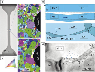
In situ TEM and ACOM were also used in small-grained Al to quantify the amount of grain rotation involved during plastic deformation. It appears that shear-coupled GB migration (SCGBM)Reference Cahn and Taylor29–Reference Han, Thomas and Srolovitz34 is the dominant mechanism despite both processes (SCGBM and grain rotation) being based on the motion of disconnections, specific GB defects that combine a step and a dislocation.Reference Han, Thomas and Srolovitz34,Reference Hirth and Pond35 Some of these disconnections involved in grain rotation are seen in Figure 2.Reference Mompiou and Legros36 These GB-based modes of deformation may become prominent in small grained materials when dislocation activity is shut down.
(a) Overview of a notched tensile sample. (b) Automated crystal orientation mapping obtained during in situ transmission electron microscopy straining of an ultrafine grain. Note: εpl, plastic strain. Al sample. (c, d) Grain growth occurs mainly through shear-coupled grain-boundary migration (SCGBM), but some grains experience relative rotation (such as grains 1 and 27). SCGBM and rotation occurs through the motion of disconnections, d. These defects are bound to the GB as they possess both a step and a dislocation character. Here, they only carry a Burgers vector b = 2a/3 [111] without step.Reference Mompiou and Legros36

The more general case encountered in metallurgy is the dislocation–GB interaction, which can be completely isolated and characterized by reducing the sample volume down to the submicron scale and selecting a given GB or twin. Using in situ techniques, the interaction mechanism can be quantified and—in rare cases—directly observed. Due to their importance in many deformation regimes, coherent twin boundaries (CTBs) have been studied in particular over the past decade, using SEM, Laue microdiffraction, and TEM.Reference Dehm, Jaya, Raghavan and Kirchlechner12
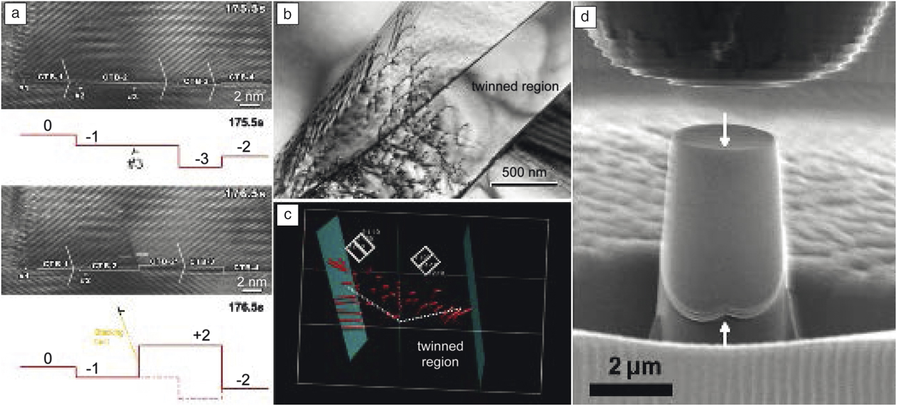
SEM studies have revealed the collective slip behavior of dislocations by analyzing the slip steps formed at a sample surface together with the (engineering) normal stress applied. For Cu samples aligned for easy slip transmission—where the dislocation can transmit in a cross-slip-like manner—a negligible stress increase for micropillars containing CTBs compared to single crystalsReference Imrich, Kirchlechner, Motz and Dehm37,Reference Liebig, Krauß, Göken and Merle38 was found. This does not necessarily imply a negligible transmission stress, as stress amplification caused by dislocation pileups cannot be excluded.Reference Imrich, Kirchlechner, Motz and Dehm37 Hence, to measure the slip transmission stress of a single dislocation through an interface, the absence of dislocation pileups needs to be proven (i.e., by synchrotron-based Laue microdiffraction with in situ capabilities).Reference Maass, Van Petegem, Van Swygenhoven, Derlet, Volkert and Grolimund39 Malyar et al.Reference Malyar, Dehm and Kirchlechner40 estimated the stress required for ideal slip transmission for Cu to be ∼17 MPa, a value remarkably close to previous estimates of the stress required for cross-slip (∼24 +/– 2 MPa).Reference Caillard and Martin41 This result was confirmed by measuring the activation volume of slip transmissionReference Malyar, Grabowski, Dehm and Kirchlechner42 for ideal slip transmission in focused ion beam (FIB)-prepared Cu (Figure 3d).
(a) Dislocation interactions and multiplication during nanoindentation of a nanotwinned Cu thin film. Reprinted with permission from Reference Reference Li, Wang, Misra, Zhang, Huang and Hirth43. © 2011 Elsevier. (b, c) Bright-field image of dislocations gliding across a coherent twin boundary (CTB) in α-Ti with (c) accompanying 3D model constructed from electron tomogram of the interaction.Reference Kacher and Robertson44 (d) Scanning electron microscope image taken during the deformation of a Cu micropillar containing a single CTB (along white arrows).Reference Malyar, Grabowski, Dehm and Kirchlechner42

The direct observation of dislocation slip-transmission processes at interfaces requires TEM. In one case, nanoindentation was performed on nanotwinned Cu thin films while imaging the dislocation behavior at high resolution.Reference Li, Wang, Misra, Zhang, Huang and Hirth43 Under certain stress conditions, CTBs were observed to act as a continuous source of partial dislocations, contributing to the strength and work-hardening behavior of the nanotwinned material (Figure 3a).
In situ TEM tensile experiments combined with electron tomographyReference Kacher and Robertson44,Reference Kacher and Robertson45 confirmed that the interaction of dislocations with CTBs depended on the crystal structure (face-centered cubic [fcc] or hexagonal close-packed [hcp]), the geometry between the incoming dislocations’ Burgers vectors and CTB plane, and the magnitude of the residual twin-boundary dislocation Burgers vector. In α-Ti, under favorable alignment of slip planes across the boundary, CTBs are essentially invisible to dislocation propagation as dislocations could transverse the boundary via a simple cross-slip-like mechanism (Figure 3b–c) similar to the observations in previous SEM investigations. Chassagne et al. observed dislocations crossing a CTB containing defects in Cu, which is often the case even in undeformed samples.Reference Chassagne, Legros and Rodney18 Although the boundary geometry permitted direct transmission, a dislocation pileup formed, suggesting either that transmission behavior varies between fcc and hcp materials, or that the defect state in the boundary affects the transmission process.Reference Chassagne, Legros and Rodney18
Kacher et al. observed, in austenitic stainless steels, that if the Burgers vector of incoming dislocations is in the plane of the CTB, the dislocations are accommodated into the boundary and glide along its plane.Reference Kacher and Robertson45 If the CTB is not a glide plane, a dislocation pileup forms and residual boundary dislocations, resulting from the misorientations between incoming and outcoming slip systems, are left by traversing dislocations, resulting in a local elastic strain buildup. This shows that even with what is considered as a simple interaction (dislocation/CTB), many questions remain depending on deformation levels and the number of slip systems involved, which is important for understanding the role of CTBs in failure initiation processes.
Beyond uniaxial and quasistatic testing
Among the efforts to expand the range of nanomechanical testing (typically, between 10–5 s–1 and 10–2 s–1), the high strain rate regime has remained mostly unexplored, primarily due to limitations of mechanical design such as resonance frequencies and data acquisition/control electronics. At the macroscale, bulk mechanical properties are measured with dedicated instruments such as dynamic tensile test setups or ballistic devicesReference Jia and Ramesh46 that have just started to approach the nanoscale.Reference Lee, Veysset, Singer, Retsch, Saini, Pezeril, Nelson and Thomas47 Several nanoindentation instruments capable of strain rates up to ∼1 s–1 have been developed, but none of them is yet widely used for measuring fundamental mechanical properties at very high strain rates.Reference Jennings, Li and Greer48
Recently, an intrinsically displacement-controlled nanomechanical testing system was developed and strain rates up to 1000 s–1 were demonstrated on nc-Ni micropillars.Reference Guillonneau, Mieszala, Wehrs, Schwiedrzik, Grop, Frey, Philippe, Breguet, Michler and Wheeler49 Considering that a displacement speed of 10 mm/s on a 1-µm-high pillar translates to a strain of 10,000 s–1, a 10 µs experiment is then sufficient to achieve 10% strain. Such short experiments reduce thermal drift problems and high strain-rate experiments at variable temperatures become easier to perform than quasi-static ones. Similar to quasistatic experiments, flow stress and strain-hardening coefficients can be determined.
In addition, activation volumes can be extracted from constant strain-rate tests, strain-rate jump tests, or stress-relaxation tests at a given test temperature. They are on the order of the atomic volume (or b Reference Vetterick, Gruber, Suri, Baldwin, Kirk and Baldo3, with b being the Burgers vector) for diffusional mechanisms such as Nabarro–Herring or Coble creep, and on the order of 1000 b Reference Vetterick, Gruber, Suri, Baldwin, Kirk and Baldo3 for dislocations moving through a dislocation forest in polycrystalline materials. For high strain-rate experiments, however, current SEMs cannot capture the deformation in situ at the highest strain rates, but SEM imaging is still required for positioning and post-experiment imaging as well as during stepwise loading applying plastic strain increments, which is often beneficial to avoid geometrical constriction.Reference Schamel, Wheeler, Niederberger, Michler, Sologubenko and Spolenak50 Further details on high strain-rate testing can be also found in the article by Barnoush et al. in this issue.Reference Barnoush, Hosemann, Molina-Aldareguia and Wheeler51
Analyzing the strain-rate sensitivity of materials is another way to sort out the mechanisms at play. Combined with automated sample preparation in focused ion beam (FIB) microscopes, the activation volume of slip transmissionReference Malyar, Grabowski, Dehm and Kirchlechner42 for ideal slip transmission has been determined for Cu (Figure 3d), as well as for high Mn steels.Reference Choi, Sandlöbes, Malyar, Kirchlechner, Korte-Kerzel, Dehm, De Cooman and Raabe52,Reference Choi, Sandlöbes, Malyar, Kirchlechner, Korte-Kerzel, Dehm, Choi and Raabe53 In nanocrystalline metals, several dislocation-based and GB-mediated mechanisms have been proposed to explain their strain-rate sensitivity.Reference Mohanty, Wheeler, Raghavan, Wehrs, Hasegawa, Mischler, Philippe and Michler54,Reference Schwaiger, Moser, Dao, Chollacoop and Suresh55 Because a single micropillar contains a large number of crystallites, measuring its mechanical properties can be carried out with quality and reproducibility comparable to regular bulk tests. Strain rates of up to eight orders of magnitudes (0.001 s–1 to 1000 s–1) were explored in a single setup on a large number of FIB-micromachined nc-nickel samples.Reference Guillonneau, Mieszala, Wehrs, Schwiedrzik, Grop, Frey, Philippe, Breguet, Michler and Wheeler49
Most of these miniaturized techniques now include high-resolution digital image correlation (HRDIC) methods that allow SEM in situ deformation tests with high spatial resolution.Reference Di Gioacchino and Quinta da Fonseca56,Reference Zhang, Lunt, Abdolvand, Wilkinson, Preuss and Dunne57 Following the evolution of slip activity in a statistically relevant number of grains, thereby unveiling competing deformation mechanisms, can thus be carried out with high confidence in engineering materials.Reference Chen and Daly58 Although the deformation properties of metals under multiaxial loading conditions differ from those predicted by uniaxial tests, the latter govern our understanding of the micromechanical behavior of materials. Several multiaxial deformation methods have been developed such as bulge pressure tests, flat punch, and cruciform tests.
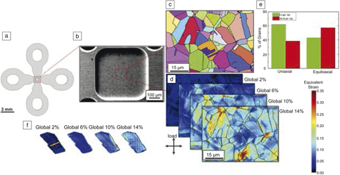
A miniaturized biaxial testing set up was developed for in situ diffraction experiments at synchrotron beamlines and in SEM chambers for HRDICReference Van Petegem, Guitton, Dupraz, Bollhalder, Sofinowski and Upadhyay59 (Figure 4). Miniaturized samples (Figure 4a–b) can be manufactured using electrochemical micromachining for HRDIC (Figure 4d) and electron backscatter diffraction (EBSD) (Figure 4c) studies.Reference Polatidis, Hsu, Smid and Van Swygenhoven60 Defect accumulation and evolving microstructures can be followed upon different loading states, or strain paths. Figure 4d shows HRDIC slip traces in a 304 stainless steel during equibiaxial loading to different global strain levels as well as the traces of an area loaded until a maximum global strain of 14% is achieved. Figure 4f shows the evolution of slip traces in one particular grain, revealing that at 10% global strain, a second slip system is activated. Careful comparison of the slip traces in several grains shows that equibiaxial loading favors martensitic transformation through the activation of multiple slip systems (Figure 4e), with slip intercepts acting as nucleation sites for martensite. The obtained information is essential to implement new physics-based (e.g., kineticReference Zecevic, Upadhyay, Polatidis, Panzner, Van Swygenhoven and Knezevic61) micromechanical models, for which constitutive equations until now have relied solely on monotonic uniaxial tests.
(a) Miniaturized cruciform-shaped sample with (b) reduced thickness in the center for (c) electron backscatter diffraction, and (d) high-resolution digital image correlation method investigation. (e) Statistical analysis showing that equibiaxial loading results in more grains exhibiting multislip activation. (f) Example of a grain at 2% global strain, initially exhibiting one slip system corresponding to the highest Schmid factor (red) and with superimposed traces of the second highest (yellow) Schmid factor that appears upon further loading (10–14% global strain) on one edge of the grain.Reference Polatidis, Hsu, Smid and Van Swygenhoven60

Overall, the combination of strain-rate sensitivity approaches, quantitative diffraction methods with in situ imaging and micromechanical testing confirm that deformation mechanisms in nanocrystalline metals are complex and do not rely on a single mechanism. And even a perfectly delimited mechanism such as dislocation–twin interaction may lead to various outputs. To gain new, additional insights into the different deformation modes, a combinatorial approach analyzing a large number of samples over various temperatures and strain rates is a promising toolset to explore complex nanomaterials or multicomponent alloys.

Josh Kacher has been an assistant professor at the Georgia Institute of Technology since 2015. He received his BS and MS degrees from Brigham Young University in applied physics in 2008, and in mechanical engineering in 2009. He received his PhD degree in materials science and engineering from the University of Illinois at Urbana-Champaign in 2012. He was a postdoctoral fellow at the University of California. His research focuses on the degradation and failure of metals and alloys in extreme environments. Kacher can be reached by email at josh.kacher@mse.gatech.edu.

Christoph Kirchlechner is a group leader for nano- and micromechanics at the Max-Planck-Institut für Eisenforschung GmbH, Germany. He studied materials science at the University of Leoben, Austria, where he also obtained his PhD degree. His current research focuses on in situ deformation, fatigue, and fracture at the micron scale combined with synchrotron-based Laue microdiffraction. He received a Promotio Sub Auspiciis Praesidentis Rei Publicae Award in 2012. In 2017, he received the Heinz Maier-Leibnitz Award of the German Research Foundation. Kirchlechner can be reached by email at kirchlechner@mpie.de.

Johann Michler has been head of the Laboratory for Mechanics of Materials and Nanostructures at Empa—Swiss Federal Laboratories for Materials Science and Technology, Thun, Switzerland, since 2000. He studied materials science in Erlangen, Germany, and received his PhD degree in 1999 from the L’Ecole Polytechnique Fédérale de Lausanne, Switzerland. His research interests include synthesis of thin films via physical vapor deposition, atomic layer deposition, electrochemical methods, and the development of advanced analytical methods to measure mechanical properties at small length scales under extreme conditions. He has authored more than 300 peer-reviewed papers and is co-founder of two startup companies. Michler can be reached by email at johann.michler@empa.ch.

Efthymios Polatidis is responsible for the neutron diffractometer POLDI at SINQ, at the Paul Scherrer Institute (PSI), Switzerland. He studied mechanical engineering at the University of Thessaly, Greece. He received his PhD degree from The University of Manchester, UK, in 2012. He completed postdoctoral research at the Max Planck Institute for Intelligent Systems, Germany, and at PSI within the European Research Council Advanced Grant (MULTIAX). His current research interests include mechanical behavior and phase transformations of engineering materials and residual stress characterization using diffraction. Polatidis can be reached by email at efthymios.polatidis@psi.ch.

Ruth Schwaiger has been head of the Nanomechanics Research Group at Karlsruhe Institute of Technology (KIT), Germany, since 2010. She studied physics at the Technische Universität Wien in Vienna, Austria, conducted her doctoral research at the Max Planck Institute for Metals Research, Germany, and obtained her PhD degree from the University of Stuttgart, Germany, in 2002. After completing postdoctoral research at the Massachusetts Institute of Technology, she joined the Forschungszentrum Karlsruhe, Germany, in 2004, and then moved to a management consulting firm in 2007. Her research interests include deformation mechanisms in materials, the mechanics of small-scale structures, biomechanics and mechanical metamaterials, and aims to develop a mechanism-based understanding of deformation and failure. Schwaiger can be reached by email at ruth.schwaiger@kit.edu.

Helena Van Swygenhoven-Moens is a full professor at École Polytechnique Fédérale de Lausanne, Switzerland, and is head of a research group at the Paul Scherer Institute, Switzerland. She studied physics at the Free University of Brussels, Belgium, and she received her PhD degree in 1983 from the Central Jury, Belgium. She conducted research with a Marie-Heim Vögtlin Grant of the Swiss National Science Foundation, Switzerland. Her research focuses on the development of in situ experiments at synchrotron and neutron facilities to study microstructures during operation and synthesis, providing synergies with computational modeling. She is a Fellow of the Materials Research Society, an elected member of the Royal Academy of Science of Belgium, and a European Research Council advanced grant holder. Van Swygenhoven-Moens can be reached by email at helena.vanswygenhoven@psi.ch.

Mitra Taheri is the Hoeganaes Chair Professor in the Department of Materials Science and Engineering at Drexel University. She leads the Dynamic Characterization Group, which focuses on the development and use of in situ microscopy tools to characterize materials for a wide variety of applications, ranging from energy to health. She received her PhD degree in materials science and engineering from Carnegie Mellon University in 2005. Before joining Drexel University in 2008, Taheri held positions as a NRC Postdoctoral Fellow at the US Naval Research Laboratory and as a Director’s Postdoctoral Fellow at Lawrence Livermore National Laboratory, as well as positions as an ONR Summer Faculty Fellow at the Naval Surface Warfare Center, and a visiting professor at Politecnico di Milano, Italy. She will move her group to Johns Hopkins University in 2020. Taheri can be reached by email at mtaheri@coe.drexel.edu.

Marc Legros has been at the Centre National de la Recherche Scientifique (CNRS), France, since 1997, first in the Laboratoire de Physique des Matériaux, and since 2002, in the Centre d’Elaboration des Matériaux et d’Etudes Structurales. He obtained his PhD degree in solid-state physics from the Université Paul Sabatier, France, in 1994. He was a postdoctoral fellow at Johns Hopkins University. His research focuses on several metallic and semiconducting compounds, for understanding deformation mechanisms observed through in situ transmission electron microscopy experiments. He received the Bessel Prize from the Humboldt Foundation in 2013, the Constellium Prize from Académie des Sciences in 2017, and the Silver Medal of CNRS in 2018. He is currently coordinating the International Research Network on the mechanics of nano-objects “Mecano.” Legros can be reached by email at marc.legros@cemes.fr.