Introduction
According to the European Joint Research Center, by 2100, the proportion of renewable energy in the total energy demand will be as high as 86%. Among the renewable energy sources, solar energy accounts for more than 60% of the total energy demand [1]. Recently, organic–inorganic halide perovskites have attracted enormous interest as a new photovoltaic material for solar cells. Since perovskite solar cells (PSCs) based on CH3NH3PbI3 were first reported with a power conversion efficiency (PCE) of 3.8% in 2009, the current PCE of PSCs has exceeded 22.1% [Reference Kojima, Teshima, Shirai and Miyasaka2, Reference Yang, Park, Jung, Jeon, Kim, Lee, Shin, Seo, Kim and Noh3, Reference Zhao, Yu, Wang, Liao, Shrestha, Grice, Cimaroli, Guan, Ellingson, Zhu, Zhao, Xiong and Yan4]. Besides the high efficiency, low-temperature solution-based fabrication routes provide an abroad prospect for flexible or tandem modules based on nonheat resistant substrates [Reference Bu, Wu, Liu, Yang, Zhou, Yu, Qin, Shi, Wang and Li5, Reference Li, Zhang, Wang, Sarvari, Liu, Wu, Yang and Wang6, Reference Zhang, Wu, Zhang, Wang, Liu, Chen, Ji, Liu, Ahmad and Chen7]. In order to realize the commercialization of PSCs, enormous efforts have been made to promote the stability of devices and upscaling [Reference Tavakoli, Tavakoli, Nourbakhsh, Waleed, Virk and Fan8, Reference Bi, Gao, Scopelliti, Oveisi, Luo, Grätzel, Hagfeldt and Nazeeruddin9]. The key to improve PCE of PSCs lies in the optimization of the perovskite layer morphology. Optoelectronic properties of perovskite such as light absorption, charge carrier diffusion length, charge transport, and recombination are directly dependent on film morphology [Reference Zheng, Zhang, Ma, Lu, Chen, Wang, Xiao and Gong10, Reference Wang, Liu, Zhang, Zhang, Ahmad, Ying, Wang, Li, Chen and Wu11, Reference Wang, Zhang, Zhang, Liu, Ji, Chen, Chen, Wu and Li12, Reference Zhang, Wu, Zhang, Waseem, Wang, Mahdi, Chen, Gao, Chen, Wu and Li13]. And as a result, various fabrication methods including anti-solvent treatment (A.S.T.), vacuum evaporation, two-step sequential deposition, vapor assisted deposition, additive-assisted deposition, spray, and doctor blade have been developed to obtain high-quality perovskite films [Reference Xiao, Kerner, Zhao, Tran, Lee, Koh, Scholes and Rand14, Reference Liu, Johnston and Snaith15, Reference Wu, Li, Han, Wang, Li, Cai, Zhou, Noda and Han16, Reference Burschka, Pellet, Moon, Humphrybaker, Gao, Nazeeruddin and Grätzel17, Reference Liu, Zhang, Yang, Yang, Ren, Pang and Liu18]. Among these approaches, anti-solvent method is well developed due to the low cost and feasible operation as well as superior PCE of PSCs.
It is well-known that anti-solvent can speed up the heterogenous nucleation via the quick extraction of solvent to leave solute. In this process, anti-solvent works on the perovskite precursor and dissolved solvent (such as DMSO, DMF, and GBL). It is interesting and meaningful to improve the quality of perovskite films via anti-solvent process and solvent engineering [Reference Wang, Li, Zhang, Liu, Gu, Sarvari, Ye, Wu, Wang and Chen19]. In 2015, Han et al. used DMSO solvent to retard the crystallization of PbI2 and thus fabricated a compact PbI2 film. However, due to the volatility of DMSO, the nucleation rate of the mesophase MAI-PbI2-DMSO is different, which leads to an uneven grain size [Reference Rong, Tang, Zhao, Zhong, Venkatesan, Graham, Patton, Jing, Guloy and Yao20]. It was demonstrated that the kinds of solvents and deposition methods seriously affect the nucleation speed during the deposition processes. In 2014, Xiao et al. screened 12 different kinds of solvents for the treatment of spinning MAPbI3 perovskite film [Reference Manda, Fuzhi, Wenchao, Yasmina, Ye, Joanne, Angus, Udo, Yi Bing and Leone21]. Anti-solvent engineering has proven to be an effective and facile way to tune the nucleation and crystal growth to obtain high-quality films. However, limited study focuses on the dependence of different anti-solvents on nucleation kinetics of perovskite and PCE of PSCs. Understanding the mechanism of different anti-solvent engineering is crucial for well controlling film morphology and improving performance of PSCs. Meanwhile, environmental-friendly anti-solvents (such as ether, isopropanol, and ethanol) are also rarely employed and investigated. Green anti-solvents have a low boiling point and solubility of perovskite precursors. They are very beneficial to protect the environment and reduce atmosphere pollution while polarity of isopropanol and ethanol can be a big issue for fabricating high performance PSCs. Thus, studying the effects of various anti-solvents with different physicochemical properties on perovskite films formation is urgent and meaningful.
In this paper, we employed six kinds of frequently used and low cost anti-solvents including toluene (Tol), chlorobenzene (CB), ether, isopropanol (IPA), ethanol (Eth), and acetone with different physicochemical properties to treat the spinning perovskite films deposited from a mixed DMSO and DMF solution. The results demonstrate that the anti-solvent shows a significant effect on the perovskite crystal growth kinetics due to different boiling points, polarities, as well as chemical groups. PSCs with the best performance prepared by using anti-solvent of ether yield an efficiency of 18.47%. The results reveal the low cost and facile anti-solvent engineering process is a promising approach for the fabrication of efficient PSCs.
Results and discussion
Figure 1(a) illustrates the preparation procedure for perovskite films by different anti-solvents. Perovskite precursor solution was first dripped on the TiO2-coated FTO glass substrate and then spun at a fixed rotation speed. Due to the evaporation of solvent during spin coating, the excess solution was spun-off and the perovskite precursor solution was gradually concentrated. Each kind of anti-solvent was then dripped onto the surface of the wet film before the precipitation of perovskite during the spin-coating process. The rapid and homogenous crystallization creates a uniform, dense, and pinhole-free high-quality perovskite thin film because of the quick precapitation.
(a) Schematic diagram of anti-solvent assisted perovskite deposition process. (b) Diagraph of boiling point versus polarity of six kinds of anti-solvents. (c) Schematic molecular structures of six kinds of anti-solvents.

As shown in Fig. 1(b), six kinds of anti-solvents with different polarities and boiling points were employed in our research. The results show that acetone is a strong polar solvent and may dissolve the precursor of perovskite recipe because the stronger polarity and nonprotic the solution is, the easier the perovskite to dissolve. Therefore, the quality of the film formed by using strong polar solution should be considerably poor. The solvent polarity of Tol, CB, and ether is relatively low to other solvents, which makes those anti-solvents popular for the preparation of perovskite films. Besides, the diagram reveals that CB has the highest boiling point, and solvents with high boiling point dry much slower during the spin-coating, leading to relatively more residual CB solution on perovskite films. Furthermore, CB also does harm to environment and human health. IPA and Eth both have a low boiling point and solubility of perovskite precursors. The polarity of these two anti-solvents is around 4 which is between the polarity of CB and that of acetone. They are very beneficial to protect the environment and reduce atmosphere pollution. In order to explore effect of boiling point and polarity on perovskite formation mechanism, we used these six kinds of solvents with different polarities and boiling points to treat perovskite as anti-solvents on a uniform platform.
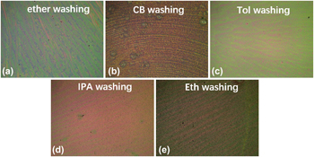
As shown in Fig. 2, un-annealed perovskite films exhibit dramatically different textures. The morphology of perovskite films is uneven and poor after treatment by the strong polar solvent acetone because the solvent will dissolve the perovskite films during this process. After treated by ether and Tol anti-solvent, radial needle-shaped crystals grow in the relatively uniform surface. With the treatment of CB, the distribution of needle crystals trends to be more homogenous and denser. There is no thermal contact between the vacuum holder of the spin-coater and the substrate. The evaporative cooling leads to micrometer scale morphology of un-annealed perovskite on the substrate. In this process, nucleation kinetics of anti-solvent method is dominant compared to crystal growth [Reference Paek, Schouwink, Athanasopoulou, Cho, Grancini, Lee, Zhang, Stellacci, Nazeeruddin and Gao22]. The needle crystals after ether and CB treatment were more homogenously distributed and denser than those from IPA and Eth treatment. Needle crystals were also obtained through IPA anti-solvent treatment. This should be owed to the quick evaporation of IPA with a low boiling point. After spin-coating, perovskite films with Eth treatment show a low quality surface, which implies an inhomogenous nucleation kinetic. The different colors of each metallographic microscope image thanks to different thicknesses of each film. The size of metallographic microscope image is 6.52 mm length and 4.89 mm width, respectively. Actually, high dissolution of perovskite precursors could result in the rough surface of perovskite films. For the case of CB, ether, and Tol, low polarity around 3 ensures the extraction of perovskite from the high polarity solvent such as DMSO and DMF. The polarity of acetone is about 5.4, which could seriously destroy the formation of perovskite crystals. So, the appropriate polarity of anti-solvent should be between 4.5 and 2.0.
Metallographic microscope images of un-annealed perovskite film treated by anti-solvents (a) ether, (b) CB, (c) Tol, (d) IPA, and (e) Eth.

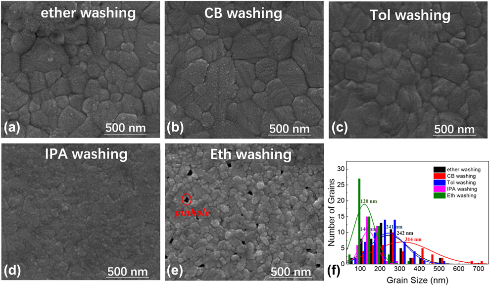
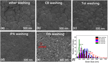
To further study the morphology of the films on a nanometer scale, scanning electron microscope (SEM) images are carried out in Figs. 3(a)–3(e). As shown in Fig. 3(e), it is obviously that the Eth prepared perovskite film exhibits some pinholes. The Eth-treated film shows a large surface inhomogeneity due to the higher polarity and lower boiling point of Eth. According to our previous discussion, polarity and boiling point can seriously affect the nucleation kinetics and the volume of residual anti-solvent. Meanwhile, Eth could decompose the perovskites. Therefore, boundaries and grain size of each CH3NH3PbI3 crystal are quite different. IPA washing procedure shows a unique phenomenon here. Grain boundaries of perovskites with IPA washing are not clear and the grain size is larger than that of perovskites with Eth washing. Luckily, perovskite films prepared by IPA washing are very dense. Low solubility of organic components and appropriate polarity are important for the high performance surface morphology of perovskite films. In comparison, perovskite fabricated by CB, ether, and Tol with lower polarities washing shows clear grain boundaries and larger grain size. These results confirm that the difference in boundaries and grain size of these films attributes to different fabrication processes. The quick separation of perovskite precursors from the solution, the formation of perovskite crystal grains, and the grain boundaries are strongly affected by the polarity and boiling point of the anti-solvent. More nuclei and quicker extraction of perovskite are formed in the washing process with the anti-solvent of low boiling point and low polarity. It is obvious that too fast anti-solvent evaporation leads to a poor extracting of perovskite precursors. As it is shown in Fig. 3, different grain sizes are obtained after treatment by these five anti-solvents. The grain size statistics of perovskite films are also shown in Fig. 3(e) (calculated by Nano Measurement software). The perovskite films treated by ether, CB, and Tol show much bigger perovskite crystals (242, 314, and 241 nm) than the others, which reduce the grain boundaries and the electronic trap states, thus facilitate the charge transport and reduce the recombination [Reference Wang, Wu, Zhang, Liu, Zhang, Ji, Gu, Chen and Li23, Reference Pathak, Sepe, Sadhanala, Deschler, Haghighirad, Sakai, Goedel, Stranks, Noel and Price24]. Poor surface morphology of perovskite films treated by IPA and Eth is attributed to relatively high polarity compared to ether, CB, and Tol, which dissolve and decompose little perovskite and perovskite precursor. Meanwhile, we observed that the boiling point is not a key factor for the extraction of perovskite precursors.
SEM top views of perovskite films treated by (a) ether washing, (b) CB washing, (c) Tol washing, (d) IPA washing, (e) Eth washing, and (f) grain size statistics of perovskite films based on each anti-solvent.

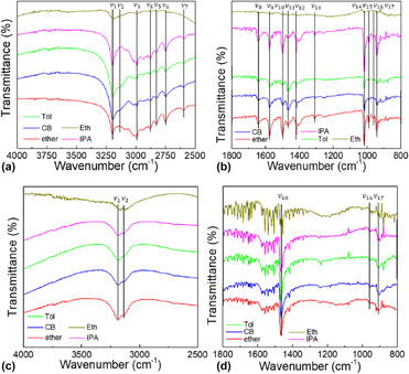
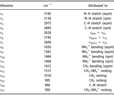
Fourier transform infrared spectrometer (FTIR) measurements were carried out to analyze the film forming process after treatment by ether, CB, Tol, IPA, and Eth washing. Here, we studied perovskite films with and without annealing as shown in Figs. 4(a) and 4(b), respectively. The FTIR measurement used transmission mode in the range of 4000–2500 and 1800–800 cm−1. It is obvious that several characteristic peaks related to N–H, C–H, NH3+, and C–N which belongs to CH3NH3PbI3 are observed in Fig. 4(a). Characteristic frequencies in the IR spectra of perovskite films were shown in Table I. The ν1 peak at 3185 cm−1 is weak for the Eth washing sample compared with this peak of samples with other anti-solvent. This result illustrates Eth could bring away organic cations and is not conductive to form high-quality perovskite. For the case of IPA or ether washing, ν3, ν6 − ν10, ν12 − ν15, ν17 are relatively high. ν3 is the asymmetric C–H stretching vibration. ν6 and ν7 are attributed to vibrational coupled modes which is ν10/11 + ν13. This improvement should be owed to the chemical nature of anti-solvent. ν8 and ν9 are asymmetric NH3+ bending, ν10 is the symmetric NH3+ bending, the enhancement of these peaks should be attributed to bending vibrations of NH3+. ν12 is the asymmetric CH3 bending mode, ν14 and ν15 are the CH3 rocking, and ν13, ν17 are the CH3–NH3+ rocking modes. In the formation process of CH3NH3PbI3, IPA and ether washing induced the bending vibration of CH3 and the rocking vibration of CH3–NH3+. We recognized the IPA and ether washing could induce stronger vibration of chemical bonds belonging to CH3NH3PbI3 in this anti-solvent. These two solvents contain CH2 and CH3 groups, and these chemical groups might react and affect the formation of perovskite crystals. It is interesting that ν16 (C–N stretch mode) was weak in IPA processed sample, which indicates there existed different functions between IPA and ether washing. After annealing, a lot of characterized peaks disappeared because of the rearrangement and recrystallization of perovskite crystals. Figure 4(b) (after annealed) shows that only ν1, ν2, ν10, ν16, and ν17 were observed in the spectrum. As in our previous discussion, ν1, ν2, ν10, ν16, and ν17 related to N–H stretch, NH3+ bending, C–N stretch, and CH3–NH3+ rocking which could represent the formation of CH3NH3PbI3. The high baselines indicate strong light absorption and light scattering.
The FTIR of un-annealed perovskite films treated by ether, CB, Tol, IPA, and Eth ranged from (a) 4000–2500 cm−1 to (b) 1800–800 cm−1. The FTIR of annealed perovskite films treated by ether, CB, Tol, IPA, and Eth ranged from (c) 4000–2500 cm−1 to (d) 1800–800 cm−1.

Characteristic frequencies in the IR spectra of perovskite films.

The UV-visible (range from 400 to 1000 nm) absorption spectra of perovskite films prepared with different anti-solvents were measured and shown in Fig. 5(a). We measured the samples with the films facing to the light. There are similar absorption spectra of perovskite films and based lines except acetone, which should be owed to its strong polarity (polarity = 5.4). Based on our previous discussion, the polarity limit that can dissolve perovskite is more than 4.5. Our results are consistent with the conclusion of Bu et al. [Reference Bu, Wu, Liu, Yang, Zhou, Yu, Qin, Shi, Wang and Li5]. It is also obvious that the absorption of perovskite films obtained via the ether and CB processes is slightly larger at ∼760 nm than that of the perovskite films prepared by using other washing solvents. This illustrates the treatment by ether or CB has a great optical absorption of perovskite films. Besides, we intercept UV-Vis absorption spectrum from 700 to 800 nm [Fig. 5(b)] to study this optical absorption in detail. Figure 5(b) shows six absorption steep slopes at 760 nm for perovskite films fabricated by anti-solvent of ether, CB, Tol, IPA, Eth, and acetone, respectively. It is interesting to find that with IPA, perovskite film achieved a relatively high absorption at 760 nm. Meanwhile, the film with Eth washing process exhibits a relatively weak absorption slope at 760 nm, which indicates that the perovskite was not formed well in this process due to the poor solubility of perovskites. However, the baseline of perovskite with IPA or Eth washing is much higher due to the diffuse reflection effect of light. Combined with our previous discussion, IPA or Eth washing leads to a rougher surface of perovskite than that with ether washing. Excessively strong polarity of anti-solvent is really bad for the morphology of perovskite. With ether, CB, and Tol treatment, perovskite films both have a good absorption slope at 760 nm. Therefore, different absorptions of perovskite should be owing to different anti-solvent extraction properties.
(a) UV-vis absorption spectra of perovskite using different anti-solvents. (b) UV-vis absorption spectra (range from 700 to 800 nm) of perovskite using different anti-solvents.

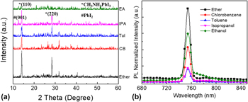
X-ray diffraction (XRD) spectra of different anti-solvent engineered perovskite films are shown in Fig. 6(a). The XRD patterns with perovskite peaks are at 14.16° and 28.1°, corresponding to the (110) and (220) planes of CH3NH3PbI3, respectively. During thermal treatment, solvent molecules are driven out of the precursors in order to form the final perovskite film. The perovskite peaks of the (110) and (220) are the sharpest and highest for the film prepared by the ether treatment. This suggests that ether can better enhance the crystallinity of CH3NH3PbI3 compared to the other anti-solvents. Because of the low boiling point and suitable polarity of ether, there is less residual anti-solvent, which is favorable for the crystallization of perovskite. Perovskite films are fabricated with IPA. CB and Tol washing all have stronger diffraction peaks of the (110) and (220) planes of perovskite, which shows well crystallization of perovskite films in these processes. However, there is an obvious (001) peak of PbI2 at 12.6° when the IPA washing process was used. This demonstrates that IPA cannot completely extract perovskite precursors during the formation of perovskite crystal. Furthermore, Eth washing process leads to more residual PbI2, which shows a stronger XRD peak of (001) at 12.6°. Although IPA and Eth are environmental-friendly anti-solvent in fabrication of PSCs, their high polarity has become a big issue. Ether with a suitable boiling point and polarity ensures the best crystallization of perovskite films.
(a) XRD patterns of perovskite films treated with different anti-solvents. (b) Steady-state absorption spectra of perovskite film prepared under different anti-solvent treatments after annealing.
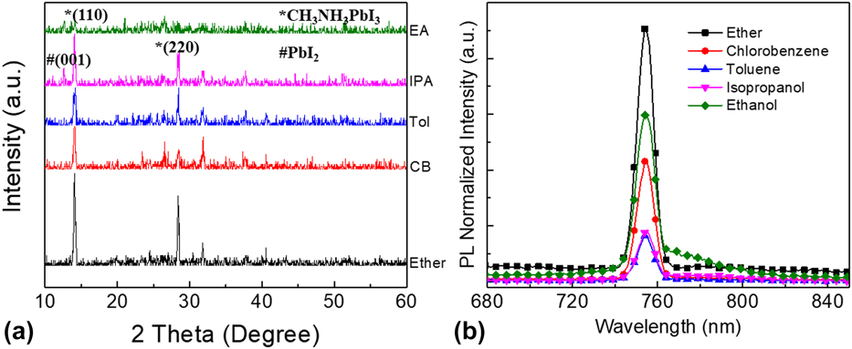
Steady PL measurement results are shown in Fig. 6(b). The perovskite films are deposited on the TiO2 films. And the film treated by ether has the highest PL intensity. Then the sequence from high to low is Eth, CB, IPA, and Tol. And the PL intensity of IPA and Tol is close. The intensity of steady PL is always associate with nonradiative charge transfer at interface and recombination [Reference Chen, Xiong, Rong, Mei, Sheng, Jiang, Hu, Li and Han25, Reference Ogomi, Morita, Tsukamoto, Saitho, Shen, Toyoda, Yoshino, Pandey, Ma and Hayase26, Reference Zuo, Gu, Ye, Fu, Wu, Li and Chen27, Reference Shih, Lan, Li, Hsieh, Wang, Wu and Lin28]. This demonstrates the lower nonradiative recombination in the crystal of ether-treated film. According to our device structure, the higher steady PL intensity means there is a lower nonradiative recombination in the crystal of ether-treated film. The treatment by ether results in high-quality perovskite film with lower trap states. Both IPA- and Tol-treated films have very weak steady PL values, which will cause a relatively poor perovskite film performance. It is observed that the PL of perovskite with Eth washing is very high due to the modification of perovskite morphology by Eth washing. This should be owed to the change of the thickness of perovskite films and the increase of diffuse reflection from rough surface. We can see that intensities of integrated steady PL spectra are also consistent with the trend of the V OC, FF, and PCE statistics.
Figure 7(a) presents the current density–voltage (J–V) curves of devices processed in different anti-solvents. The sample fabricated with the ether exhibits the best PCE, which is 18.47%. Such high PCE should be attributed to a lower charge recombination in perovskite film. This result is also consistent with the previous UV-Vis absorption and XRD analysis. The best PCEs under optimized conditions for perovskites with ether, CB, Tol, and IPA are 18.47%, 14.11%, 14.95%, and 8.13%, respectively. Besides, the fill factors of these PSCs based on four kinds of anti-solvents are 71.59, 63.20, 73.46, and 55.44%. The improved performance of the PSC with Ether or toluene is mainly attributed to the increased fill factor. The lower PCE of IPA-treated films can be explained by the SEM images in Fig. 3. We can see that the number of grain boundaries is slightly larger with IPA treatment, which will increase the charge recombination inside the device. The external quantum efficiency (EQE) for the ether-treated solar cell is shown in Fig. 7(b). The perovskite shows a wide photoresponse from 300 to 800 nm, suggesting that solar light can be efficiently collected by the terminal electrode and be converted to charge carriers, which results in the high photocurrent density of the PSC. Meanwhile, the estimated J SC value was in good agreement with the J SC values from the J–V measurement.
Statistics of parameters obtained from each anti-solvent treatment. (a) J–V curves of the solar cell samples with ether, CB, Tol, and IPA. (b) EQE spectra of ether treated PSC. Distribution of the (c) efficiency, (d) J SC, (e) V OC, and (f) FF of the devices with different anti-solvents processes.

Figures 7(c)–7(f) show parameter (PCE, J SC, V OC, and FF) statistics of devices processed by using different anti-solvents. It is clear that PCE, J SC, V OC, and FF all exhibit a similar trend with the result illustrated in Fig. 4(b). The difference is reflected in the contact quality with hole transport layer (HTL) and the morphology of perovskite, which determines the series resistance (R S) and parallel resistance (R SH) of the total device, respectively. As shown in Fig. 7(d), the sample treated by ether has a relatively high current density (J SC), which illustrates ether treatment can reduce the recombination significantly. It is reported that V OC and FF can reflect the junction properties of PSCs [Reference Dong, Xu, Shi, Li, Luo, Meng and Chen29]. Higher V OC and FF lead to an improvement of PCE, which are attributed to the enhancement of the quality of perovskite films. We also observe that the distribution of these parameters of PSCs with IPA washing is more concentrated and uniform. This confirms IPA anti-solvent washing has a useful modification for CH3NH3PbI3 films.
Conclusion
In this study, we optimized anti-solvent treatment for perovskite film crystallization. The results demonstrate that anti-solvents with both low boiling point and good polarity lead to high-quality PSCs. Besides, some chemical groups (such as CH2 and CH3) in anti-solvent (IPA and ether) also induced stronger vibration of chemical bonds and then affected the formation of perovskite. The polarity of anti-solvents plays a crucial role in the solubility of solution (DMF/DMSO). Furthermore, low boiling point creates a suitable environment for perovskite film on the spin substrate to evaporate the mixed anti-solvent and solution solvents (DMF/DMSO) fast and effectively. The PCE of PSCs exhibits a best performance of 18.47% by using ether as an anti-solvent.
Experimental methods
Device fabrication
FTO glass substrates were cleaned sequentially in alkaline detergent, acetone, ethanol, and DI water for 15 min each, followed by drying with N2 flow. A compact layer of TiO2 was deposited via spray pyrolysis at 500 °C from a precursor solution of titanium diisopropoxide bis (acetylacetonate) in ethanol (volume ratio, 1:39). The films were annealed at 500 °C for 20 min and then cooled down to room temperature. The mesoporous TiO2 scaffold was spin-coated at 4000 rpm for 30 s and annealed at 500 °C for 20 min, in which the pristine paste was diluted in ethanol (weight ratio, 1:5). CH3NH3PbI3 was synthesized using the one-step spin-coating method and the following experiments except for gold deposition were carried out in a glove box in nitrogen. The perovskite solution contains 691.5 mg PbI2, 238.5 mg MAI in 0.945 mL DMF, and 0.1065 mL DMSO, and stirred more than 2 h. 80 μL perovskite solution was spin-coated at 4500 rpm for 30 s. The anti-solvent was poured on the samples at the end of 25 s. The samples were annealed at 110 °C for 1 h. The substrates were subsequently covered with a 72.3 mg/mL solution of spiro-OMeTAD in 1 mL chlorobenzene with 28.8 μL of added 4-tert-butylpyridine, 17.5 μL of a stock solution of 520 mg/mL lithium bis(trifluoromethylsulphonyl)imide in acetonitrile, and 29 μL of 520 mg/mL tris(2-(1H-pyrazol-1-yl)-4-tert-butylpyridine) cobalt(III) bis (trifluoromethylsulphonyl) imide in acetonitrile. This solution was spin-coated at 4000 rpm for 30 s. Finally, 80 nm of a gold film was deposited using thermal evaporation.
Measurement and characterization
X-ray diffraction (XRD) diagrams were carried out using a Bede D1 system (Scientech, Shanghai, China) with Cu Kα radiation. Scanning electron microscope (SEM) images were obtained using field emission fitting SEM (FEI-Inspect F50, Holland, Thermo Fisher Scientific, Massachusetts). The UV-vis absorption spectrum was measured by an ultraviolet-visible (UV-vis) spectrophotometer (Schimadzu UV-3101 PC, Shimadzu, Kyoto, Japan). Current–voltage measurements were carried out using Keithley 2400 (Keithley, Austin, Texas) under AM 1.5 G illuminations (1000 W/m2) from a solar simulator (Newport Oriel Solar 3 A Class AAA, 64,023 A). The AM 1.5 G sun light (100 mW/cm2) was calibrated using a standard Si-solar cell (Oriel, VLSI standards, Newport Corporation, Wuxi, China). Metallographic microscope images were carried out by MZ5000 (Jiangnan Yongxin, Jiangnan Yongxin, Nanjing, China). Steady PL curves were measured by F-4600 Fluorescence Spectrophotometer (HITACHI, Tokyo, Japan). FTIR iS50R was used to measure our Fourier transform infrared (FTIR) spectroscopies.
Acknowledgments
This work was supported by the National Natural Science Foundation of China under Grant Nos. 61421002, 61574029, 61471085, and 61474015.