Introduction
In recent years, reconfigurable antennas have garnered significant attention due to their ability to adapt to complex wireless communication environments [Reference Hossain, Rahman and Murshed1–Reference Muthuvel, Shaw and Choukiker8]. These antennas are classified into three main types based on their performance characteristics: polarization-reconfigurable antennas, pattern-reconfigurable antennas, and frequency-reconfigurable antennas. Each type addresses specific challenges in wireless communication. Polarization-reconfigurable antennas, in particular, offer valuable capabilities by dynamically switching between different polarization states such as linear polarization (LP), left-hand circular polarization (LHCP), and right-hand circular polarization (RHCP). This versatility is critical for optimizing signal quality in diverse electromagnetic conditions, which is essential for ensuring robust communication systems. By minimizing interference and effectively managing complex signal paths, these antennas enhance network reliability and throughput [Reference Zhang, Jiao and Zhang9, Reference Al-Yasir, Abdullah and Ojaroudi Parchin10]. The adaptability of polarization-reconfigurable antennas not only improves signal reception and transmission but also contributes to better overall performance in challenging wireless environments. This makes them indispensable tools for achieving reliable and efficient communication systems in modern wireless networks.
Due to the superior performance of polarization-reconfigurable antennas, many researchers have conducted extensive research in this field in recent years [Reference Zhang, Zhang and Huang11–Reference Wang, Yang and Geyi14]. They are dedicated to improving the performance of these antennas and enhancing their ability to adapt to different communication environments. Polarization-reconfigurable antennas mainly include LP reconfigurable antennas, CP reconfigurable antennas, and hybrid reconfigurable antennas. Antennas capable of switching between different LP states are known as LP reconfigurable antennas [Reference Tran, Nguyen-Trong and Le15–Reference Chen, Liu and Chen17]. The work in [Reference Chen, Liu and Chen17] investigates an antenna capable of switching among seven distinct LP states without altering its performance, achieved through a multi-layer structure. But the antenna can only operate in LP mode, the anti-interference ability is weak and the use range is narrow. On the other hand, antennas that can switch between different CP states are referred to as CP reconfigurable antennas. Compared to general LP reconfigurable antennas, CP reconfigurable antennas exhibit stronger interference resistance and help eliminate multipath effects [Reference Lee and Sung18, Reference Ye, Li and Zhang19]. Ye QC et al. [Reference Ye, Li and Zhang19] proposed a reconfigurable CP array with enhanced axial-ratio (AR) bandwidth and high gain, achieved through the control of two PIN diode switches loaded on the slot and a simple DC bias design. However, for this antenna, when the incoming wave is an LP wave, although it can be received, it will lose half of its energy. Additionally, antennas capable of switching between CPs and LPs are classified as hybrid reconfigurable antennas. These antennas offer enhanced adaptability to polarization and are well-suited for complex communication environments and demands, garnering significant attention [Reference Lee and Sung20–Reference Li, Shi and Xu26]. Tran HH and Park HC [Reference Tran and Park21] introduced a simple high-gain diversity Fabry-Perot resonator antenna that alternates between CPs and LPs via PIN diode switching. However, the impedance bandwidth of the antenna is narrow, which cannot meet the needs of modern broadband communication.
In this paper, a hybrid polarization-reconfigurable antenna is proposed. The antenna utilizes a stepped coplanar waveguide (CPW) structure for feeding, with a monopole section in the center connected to four horizontal branches via PIN diodes. By selectively switching the PIN diodes between ON/OFF states within the radiation structure, the antenna can be reconfigured to operate in LHCP, RHCP, and LP. The design of the antenna is characterized by its simplicity and compactness, facilitating easy integration and requiring fewer components for structure reconfiguration. It exhibits wide impedance and AR bandwidths. Experimental measurements demonstrate that the antenna effectively covers the 2.4-GHz WLAN band (2400 to 2480 MHz) and the LTE TD 2300 band (2300 to 2400 MHz), making it highly suitable for diverse wireless communication environments.
Polarization-reconfigurable antenna design
Antenna structure
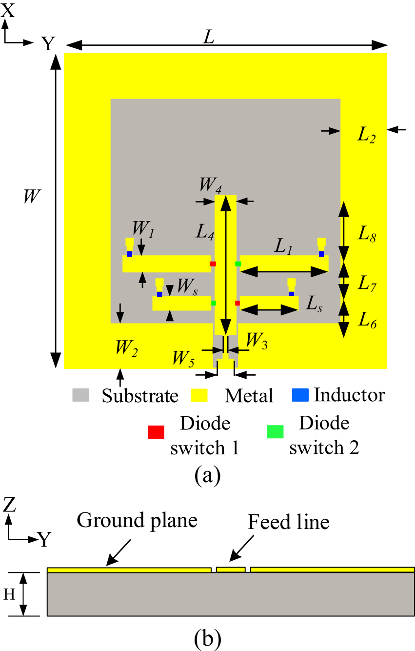
Figure 1 illustrates the detailed structure and overall geometric shape of the polarization- reconfigurable antenna designed in this work. The antenna features a simple structure and mainly comprises a dielectric substrate and an upper-layer radiating element. The dielectric substrate is constructed from FR4 with a thickness of 1.6 mm, a relative dielectric constant of 4.4, and a loss tangent of 0.02. The overall dimensions of the antenna are 70 × 70 × 1.6 mm3. The antenna is fed by a CPW, and its central monopole is connected to four horizontal stubs via PIN diodes. The CPW features a stepped structure to ensure good impedance matching. Specifically, the lower section connected to the SMA connector measures 0.7 × 5 mm2, the middle section measures 5 × 0.7 mm2, and the upper section measures 32 × 6 mm2, resulting in a total length of 37.7 mm.
Structure of polarization-reconfigurable antenna. (a) Top view. (b) Side view.

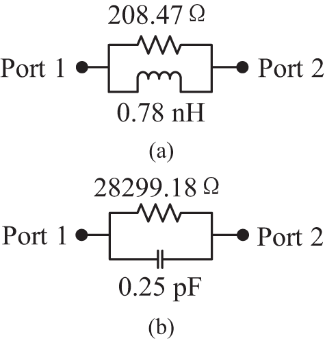
Four PIN diodes, SMP1340-079LF from Skyworks [27], are integrated between the horizontal branches and the monopole to control their connectivity. In Fig. 1, diode switch 1 (S1 and S2) denotes two switches in the same state, while diode switch 2 (S3 and S4) indicates another pair of switches in the same state. For diode switch 1, the side near the monopole acts as the cathode, and the side near the horizontal branches serves as the anode. Conversely, for diode switch 2, the side near the monopole is the anode, and the side near the horizontal branches is the cathode. The equivalent circuit models for the diodes when ON and OFF are established using the TRL calibration method. When the diode is ON with a bias current of 100 mA, it exhibits an equivalent circuit consisting of a parallel inductor of 0.78 nH and a resistor of 208.47 Ω. When the diode is OFF, its equivalent circuit comprises a resistor of 28,299.18 Ω in parallel with a capacitor of 0.25 pF. These equivalent circuit models are employed in the HFSS simulation, as depicted in Fig. 2.
Equivalent circuit model of PIN diode. (a) ON state. (b) OFF state.

The DC bias circuit for the diode is located at the end of the horizontal stub and is connected to the diode through a pad. To prevent RF signals from leaking through the bias circuit and affecting the antenna, a 120-nH surface-mount inductor is installed. In practical circuit design, the DC bias circuit at the end of the diode’s horizontal stub connects to the DC voltage source via a 120-Ω resistor. There is no additional pad required on the other side of the switch, specifically on the microstrip feed line side. Instead, a bias tee directly applies the DC signal to the PIN diode, isolating it from the simultaneously fed RF signal. This setup helps minimize the impact on antenna performance [Reference Sun, Hu and Ren28] and reduces measurement errors [Reference Lee and Sung20], establishing a well-defined DC bias. In addition, the bias tee model used in measurements is the ZX85-12 G-S+.
Antenna analysis and design
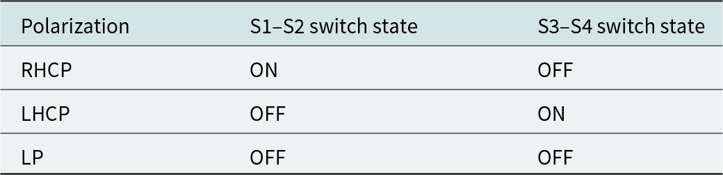
To excite CP, two orthogonal electric fields with the same amplitude and 90° phase difference are required. For the antenna, by optimizing the structural parameters of the feeding line and horizontal branches, and turning off the diode according to Table 1, the phase difference between the two orthogonal electric field components Eϕ and Eθ can be set to 90°, and their amplitudes can be adjusted to be equal. Then, the superposition of electric field components can be expressed as
 \begin{equation}\overrightarrow E = j{\text{|}}{E_\phi }|\hat \phi + |{E_\theta }|\hat \theta\end{equation}
States of the PIN diodes at different polarizations

which indicates an LHCP field. Similarly, changing the state of a diode, a RHCP will be generated with a total electric field as
 \begin{equation}\overrightarrow E = j{\text{|}}{E_\phi }|{{\text{e}}^{j\pi }}\hat \phi + |{E_\theta }|\hat \theta \end{equation}
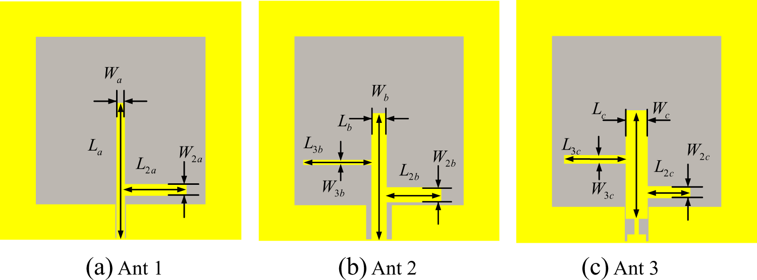
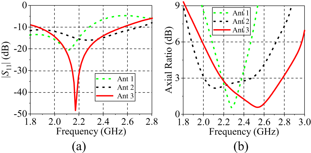
Figure 3 illustrates the evolutionary stages of the proposed antenna design with corresponding dimensions as shown in Table 2, while Fig. 4 depicts the corresponding antenna performance. In the initial antenna design (Ant 1), CP could not be achieved due to conflicting current distributions between the feed line and the left and right ground planes. Subsequently, horizontal branches were added, producing orthogonal current components between the feed line and branches, where the feed line current lagged 90 degrees behind the vertical branch currents. Adjusting the antenna dimensions to balance these current components effectively enabled the excitation of RHCP. However, this design exhibited a narrow AR bandwidth and relatively poor overall antenna performance. To enhance performance, a branch was added to the upper left side in Ant 2, along with adjustments to antenna dimensions to broaden the AR bandwidth. Nevertheless, in its LP configuration where all branches are disconnected, the antenna showed poor impedance bandwidth performance, failing to meet required frequency range criteria. To address these challenges, Ant 3 incorporated modifications to the middle section of the feed line, adopting a stepped structure. This enhancement significantly improved LP performance and further expanded the AR bandwidth for CP modes.
Design steps of the proposed antenna, (a) ant 1, (b) ant 2, (c) ant 3.

Simulated results of ant 1–3. (a) S-parameters. (b) AR.

Dimensions of ant 1, ant 2 and ant 3

Finally, additional branches were integrated into Ant 3, accompanied by the introduction of diodes to achieve polarization reconfigurability. Through iterative optimization of antenna parameters, the design depicted in Fig. 1 was achieved.
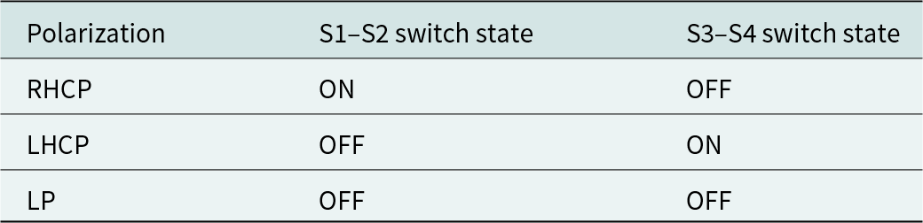
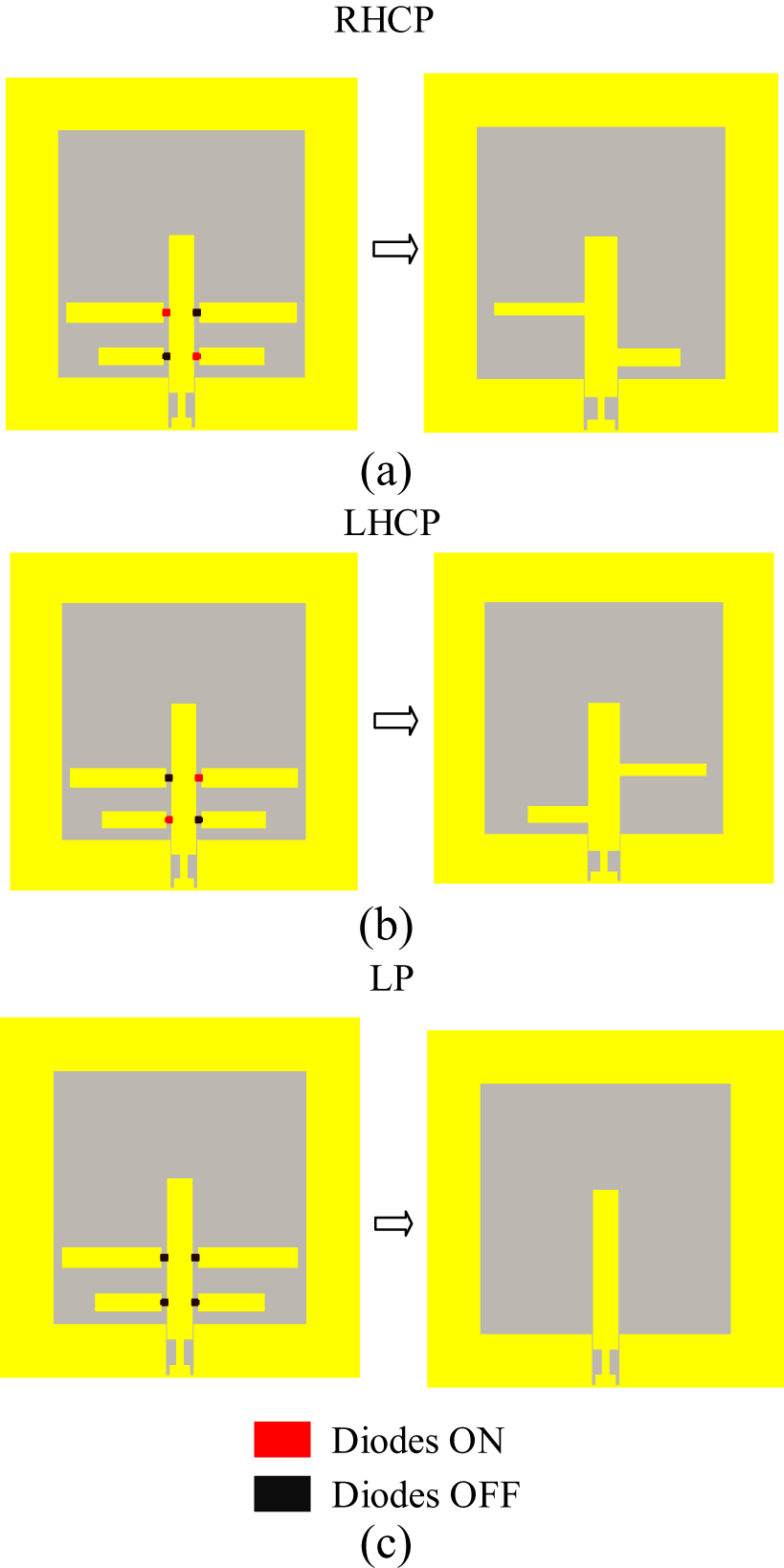
To analyze the operating principle, equivalent structures of the antenna in different states are depicted in Fig. 5, with the main radiation direction denoted as +Z. When a positive DC voltage is applied to the feeding line and a negative voltage is applied to diode switch 1 and diode switch 2 connected to the horizontal branches, diode switch 1 conducts while diode switch 2 remains off. This configuration causes the antenna to radiate RHCP waves, illustrated in the equivalent model in Fig. 5(a). Similarly, when both switches of diode switch 1 are in the cutoff state and both switches of diode switch 2 are in the conducting state, the antenna radiates LHCP waves, as shown in the equivalent model in Fig. 5(b). In the LP state, where both diode switch 1 and diode switch 2 are in the cutoff state, the antenna radiates LP waves. The equivalent model for the LP state is depicted in Fig. 5(c). Table 3 summarizes the different states of the PIN diodes corresponding to each polarization state.
Equivalent structures of the antenna in different states. (a) RHCP. (b) LHCP. (c) LP.

States of the PIN diodes at different polarizations

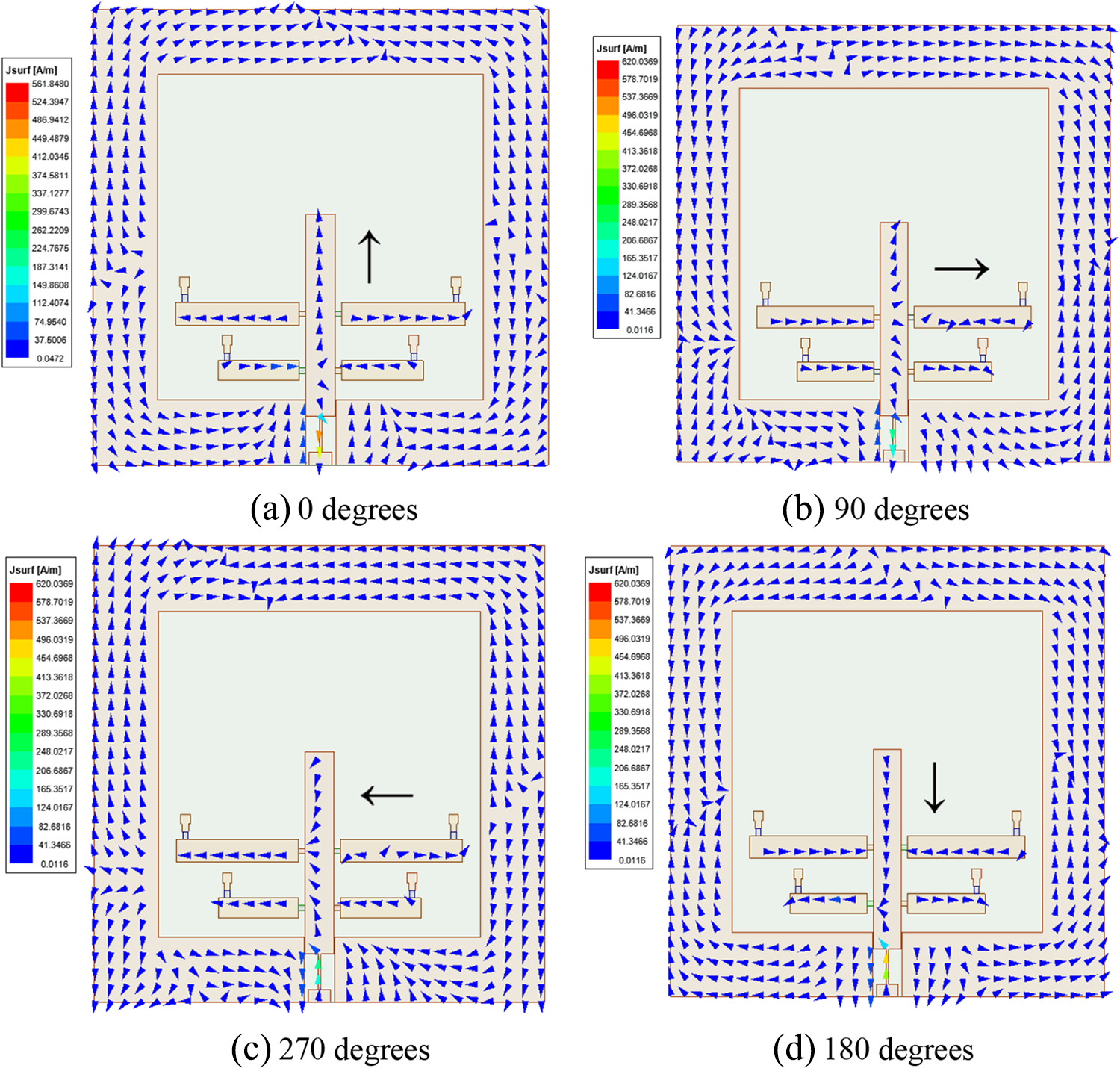
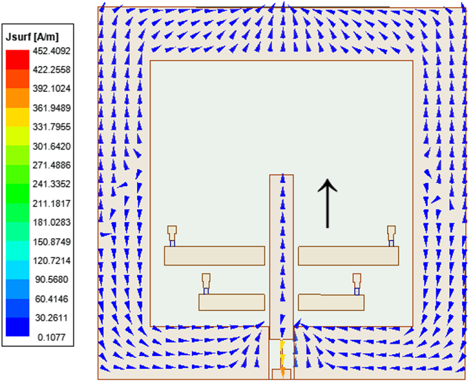
To further analyze the polarization characteristics enabled by the proposed antenna, Fig.6 illustrates the distribution of surface currents at different phases within one cycle at 2.45 GHz under the LHCP state. For simplicity, the current vector diagram for the RHCP state is omitted due to the symmetry of the antenna structure. As depicted in Fig. 6, when PIN diode switch 1 is OFF and switch 2 is ON, the electric field vector exhibits a counterclockwise rotation of LHCP radiation in the +Z direction. Fig. 7 displays the surface current distribution under the LP state, demonstrating the radiation of vertically polarized waves in this configuration.
Simulated current distribution of proposed antenna working at 2.4 GHz when switched to LHCP. (a) 0 degrees. (b) 90 degrees. (c) 270 degrees. (d) 180 degrees.

Simulated current distribution of proposed antenna working at 2.4 GHz when switched to LP.

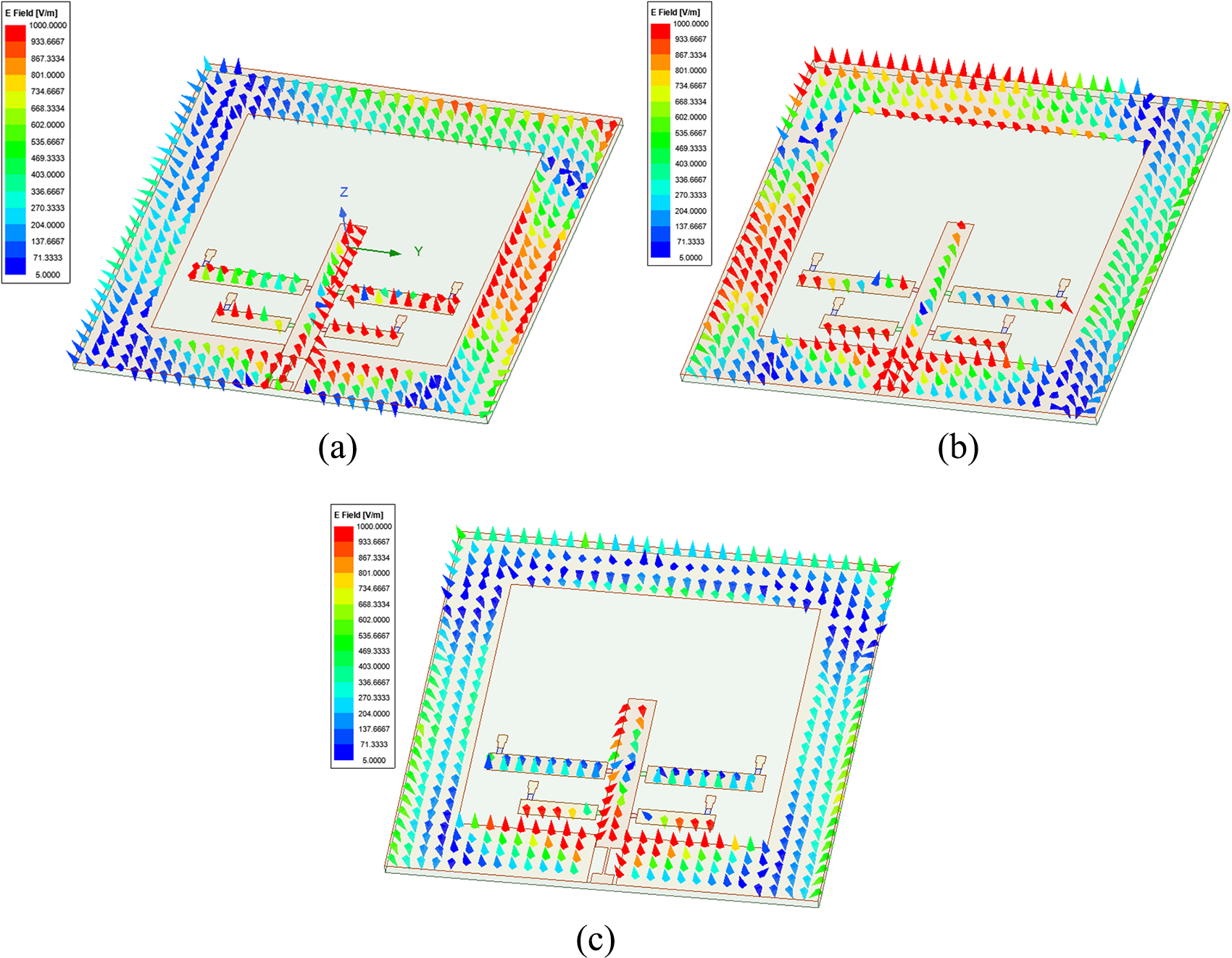
To illustrate the electric field behavior of the proposed antenna across different polarization states, Fig. 8 show the electric field distributions for LHCP, RHCP, and LP, respectively. Fig. 8(a) demonstrates a well-defined circular pattern with consistent phase rotation for RHCP. Fig. 8(b) shows a similar circular pattern but with opposite phase rotation for LHCP. Fig. 8(c) displays a linear electric field distribution, indicating strong and consistent LP. These figures highlight the antenna’s ability to support multiple polarization states effectively.
Simulated electric field of proposed antenna working at 2.4 GHz (a) RHCP. (b) LHCP. (c) LP.

Antenna parameter optimization
Structural parameters play crucial roles in influencing the polarization characteristics of an antenna. Studying these parameters is essential for optimizing antenna performance. Simulations have demonstrated that variations in the size of W 3 in the stepped feed structure, as well as the lengths of the upper horizontal branch L l and lower horizontal branch LS, have substantial impacts on the antenna’s reflection coefficient and AR. Due to the antenna’s symmetrical structure, the results for LHCP closely mirror those for RHCP. For clarity, only the LHCP results are presented here. Unless otherwise stated, when changing one parameter, all other parameters remain at their initial values.
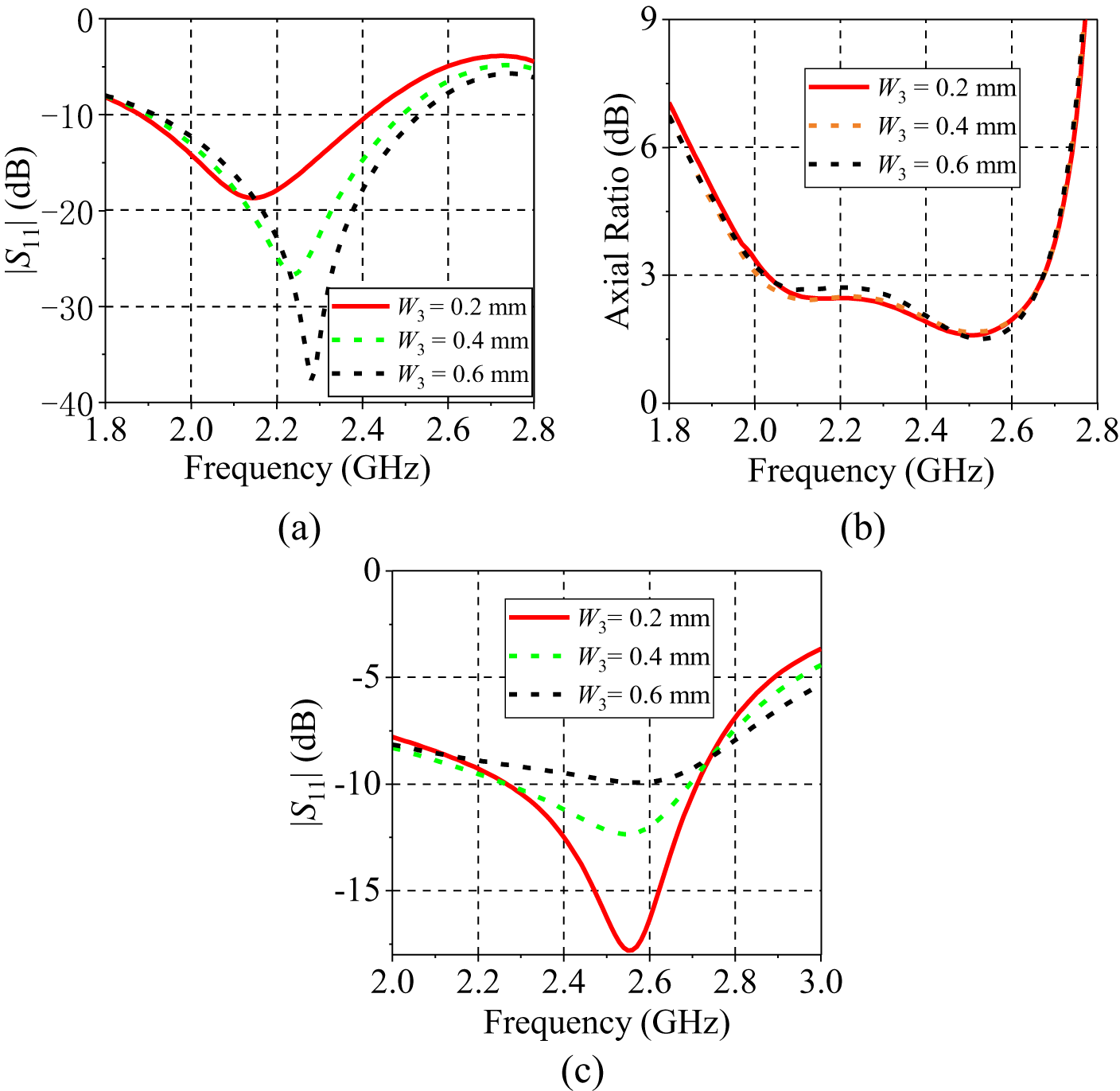
The middle section of the CPW feed line functions as an impedance transformer, where adjusting its width W 3 ensures optimal impedance matching. As shown in Fig. 9, W 3 has negligible impact on the AR of CP, but it does affect the S-parameters for both CP and LP. A narrower W 3 improves impedance matching for LP configurations. Through optimization using HFSS software, the final W 3 size was determined to be 0.4 mm.
The effect of W 3 on the antenna. (a) S-parameters of LHCP. (b) AR of LHCP. (c) S-parameters of LP.

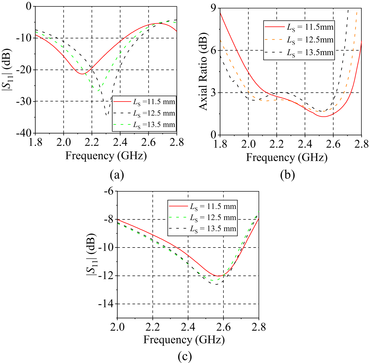
Figure 10 depicts the variation in antenna performance with changes in the length of the lower horizontal branch L S. It is evident that choosing L S to be 12.5 mm enhances the AR of CP.
The effect of L S on the antenna. (a) S-parameters of LHCP. (b) AR of LHCP. (c) S-parameters of LP.

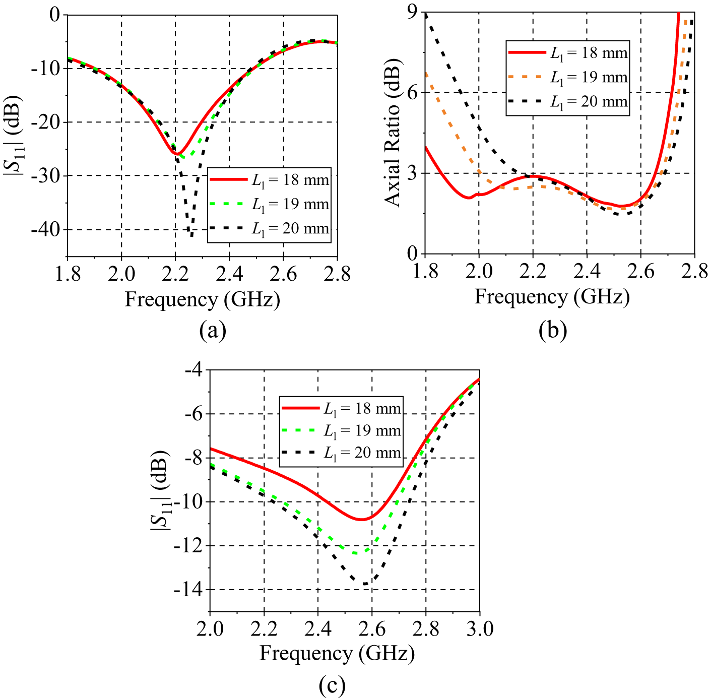
Figure 11 illustrates the impact of the length of the upper horizontal branch L l on both CP and LP. Despite being disconnected from the feed structure in the LP state, L l still affects the impedance bandwidth of LP. Larger values of L l lead to poorer impedance matching for LP. Conversely, for CP, reducing L l results in diminished AR performance. Therefore, a balanced consideration sets the length of the horizontal branch, L l, at 19 mm.
The effect of L l on the antenna. (a) s-parameters of LHCP. (b) AR of LHCP. (c) S-parameters of LP.

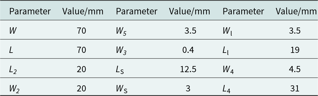
In addition to the parameters mentioned above, other structural aspects of the antenna also play a critical role, such as the length and width of the central feeding part. These dimensions significantly influence impedance matching for LP and AR performance for CP. Adjusting these parameters is essential to achieve optimal performance for both CP and LP simultaneously. Through optimization using Ansoft HFSS software, the final dimensions of the optimized antenna are detailed in Table 4.
Dimensions of the optimized antenna

Experiments and results
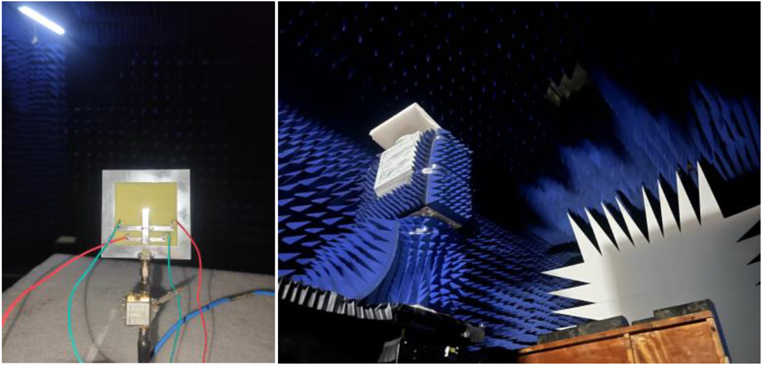
Based on the simulations, the proposed polarization-reconfigurable antenna was fabricated, whose photograph is shown in Fig. 12. A vector network analyzer was used to measure the S-parameters and to calibrate the system. The receiving antenna was positioned at a fixed distance from the DUT to capture the far-field radiation patterns. The measurement setup for the far-field measurements is shown in Fig. 13 below. Measurement involved various parameters, such as S-parameters, AR, normalized radiation patterns, and gains in different polarization states. These measurement results were then compared with those obtained from simulations.
Photograph of the fabricated antenna.

Photograph of the measurement setup for the far-field measurements.

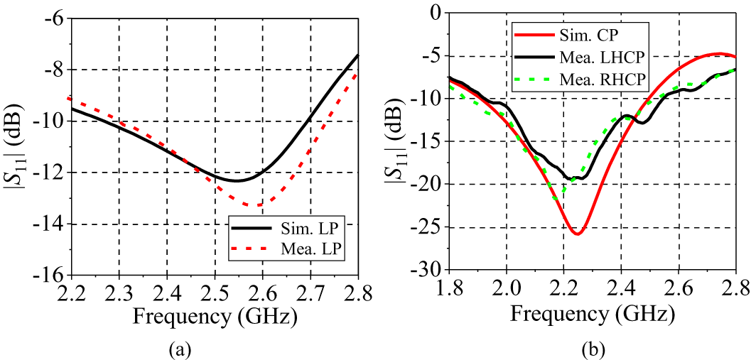
Figure 14 presents both the measured and simulated results of the antenna’s S-parameters. As shown in Fig. 13(a), in LP mode, the measured impedance bandwidth (|S 11| < − 10 dB) is 15.93% (2.31–2.71 GHz), while the simulated one is 16.94% (2.27–2.69 GHz). As illustrated in Fig. 13(b), in CP mode, the measured impedance bandwidth for LHCP (|S 11| < − 10 dB) is 27.8% (1.92–2.54 GHz), while for RHCP it is 30.7% (1.85–2.52 GHz). The simulated impedance bandwidth for CP (|S 11| < − 10 dB) is 27.3% (1.9–2.5 GHz). The measured results exhibit slight deviations from the simulations, which can be attributed to the fabrication tolerance of the antenna and the influence from the DC bias circuit.
Simulated and measured S-parameters of the antenna at different states. (a) LP state. (b) CP states.

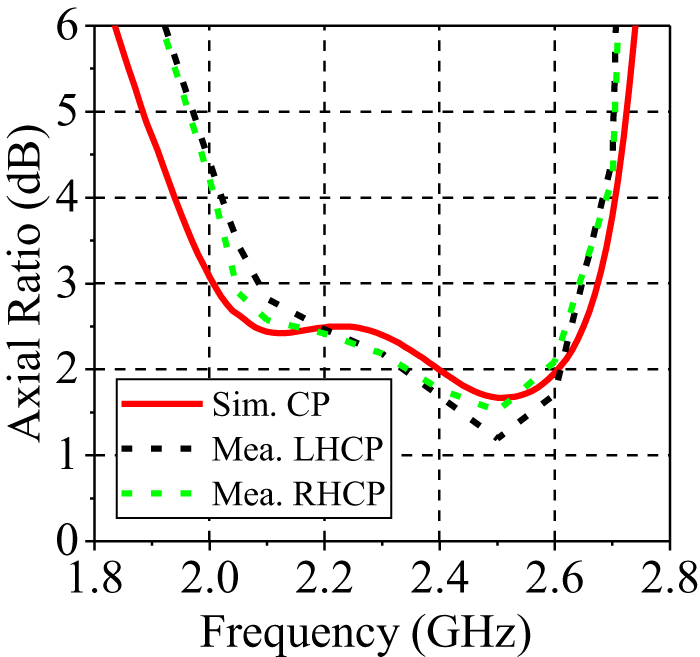
Figure 15 presents the measured and simulated results for the AR of the antenna in CP mode. In the LHCP mode, the measured 3-dB AR bandwidth is 22.4%, covering the 2.1–2.63 GHz frequency range. In the RHCP mode, the measured 3-dB AR bandwidth is 25.2%, covering the 2.05–2.64 GHz frequency range. The simulated AR bandwidth for CP is 27.9%, covering the 2–2.67 GHz frequency range. It can be seen that the AR results from simulation and measurement are generally consistent. From this, the overlap bandwidths for impedance bandwidth and AR bandwidth in LHCP and RHCP states are measured as 18.96% and 20.5%, respectively. Clearly, this antenna exhibits excellent CP performance, with its 3-dB AR bandwidth covering the 2.4-GHz WLAN band.
Simulated and measured ARs of the antenna at CP states.

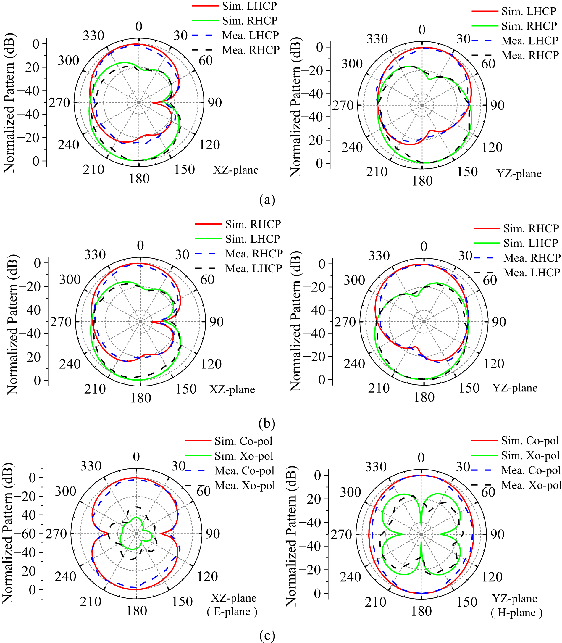
Figure 16 presents the measured and simulated normalized radiation patterns of the antenna at 2.45 GHz for three different polarization states in the XZ- and YZ-planes. From the CP patterns, it is evident that the antenna radiates along the ±Z axis, with stable measured radiation patterns. The LHCP pattern shows good broadside radiation patterns at the two main radiation directions, while the corresponding cross-polarized RHCP also exhibits similar patterns in the opposite directions. For the LP state, the measured and simulated patterns display distinct directional radiation along the XZ- and YZ-planes, indicating effective LP. On the H-plane, the four branches generate a current along their length direction, which excites a certain amount of radiation, leading to a higher cross-polarization. In contrast, on the E-plane, the current formed by the width direction of the four branches is relatively small, resulting in a lower cross-polarization.
Simulated and measured normalized radiation patterns of the antenna at 2.45 GHz at different states. (a) LHCP state. (b) RHCP state. (c) LP state.

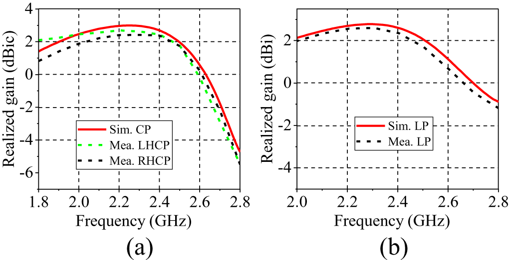
The measured and simulated gains of the antenna are shown in Fig. 17. It can be seen that the antenna maintains a stable gain across all three states. When the antenna operates in LHCP and RHCP modes, the measured gains are nearly identical. In LHCP, RHCP, and LP modes, the antenna’s measured maximum gains are 2.68 dBic, 2.42 dBic, and 2.6 dBi, respectively. The discrepancies between the simulated and measured gains are primarily due to limitations in antenna manufacturing precision, soldering of PIN diodes and capacitors, and imperfections in the measurement system. In addition, efficiency of the antenna at 2.45 GHz for different polarization states is shown in Table 5 below. It can be seen from the table that the efficiency of the measured antenna is greater than 83% under the three polarizations.
Simulated and measured realized gains of antenna at each state. (a) CP state. (b) LP states.

Efficiency of the antenna at 2.45 GHz for different polarization states

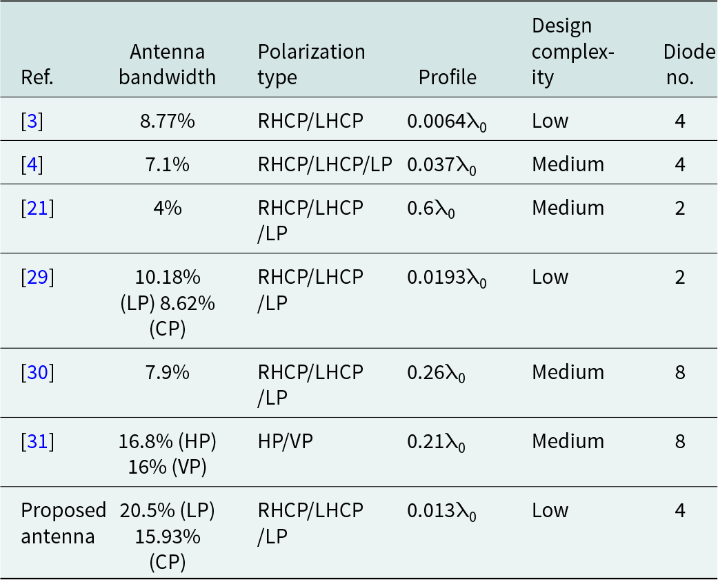
Table 6 provides a performance comparison between the proposed and the previous similar reconfigurable antennas. It can be seen from Table 5 that the comparison is made in terms of antenna bandwidth, polarization states, profile, design complexity, number of PIN diodes. In the comparison, antenna bandwidth refers to the overlap between AR and impedance bandwidths of the antenna at the CP mode, while it represents the impedance bandwidth for the LP mode. HP refers to horizontal polarization, and VP means vertical polarization.
Performance comparison between the proposed and the previous reconfigurable antennas

From the comparison, the proposed antenna provides a higher bandwidth, ensuring robust performance over a wide frequency range. It supports versatile polarization types, including RHCP, LHCP, and LP, making it adaptable to various applications and environments. The compact profile of 0.013λ0 makes it ideal for space-constrained applications such as portable devices and integrated circuits. Additionally, its low design complexity reduces manufacturing costs and makes it suitable for mass production. With four diodes, it achieves an optimal balance between performance and complexity, providing efficient operation without unnecessary intricacy. These features make the proposed antenna a highly competitive and versatile solution for modern communication systems.
Conclusion
This paper presents a compact, low-profile CPW-fed antenna designed for reconfigurable polarization, using four PIN diodes to switch between LHCP, RHCP, and LP states. Measurements demonstrate a LP impedance bandwidth of 15.93%, with AR and impedance bandwidths of 18.96% for LHCP and 20.5% for RHCP modes. This configuration effectively covers the 2.4-GHz WLAN system (2400–2480 MHz) and the LTE-TD 2300 band (2300–2400 MHz), meeting diverse wireless communication requirements. All the results validate the antenna’s consistent performance across different polarization states, enhancing its suitability for applications in consumer electronics and industrial communication systems.
Acknowledgement
This work was supported by the Fundamental Research Funds for the Central Universities (Grant No. B220202083).
Competing interests
The authors report no conflicts of interest.

Yang Wu received the B. S. degree in electric information engineering from Hunan University of Technology, Changsha, Hunan, China, in 2022. From September 2022, she is a master student of Nanjing University of Information Science and Technology, Nanjing, Jiangsu, China. Her research interests include broadband and multiband antennas, miniaturized and integrated antennas, and reconfigurable antennas.

Ningning Lu is a senior engineer and institute-level expert at the 54th Research Institute of China Electronics Technology Group Corporation (CETC), graduated from Beijing Jiaotong University with a specialization in Communication and Information Systems. His research focuses on IoT, cableless information networks, and integrated space-ground networks, where he has pioneered advancements in ultra-low-power IoT technologies. With 6 authorized invention patents, over 10 academic publications, and recognition as a Third-Tier Talent in Hebei Province’s “Three Three Two” Talent Project’ (2017), he demonstrates expertise in driving innovation across communication systems and next-generation network architectures.

Rui Ren received the Ph.D. degree in optical engineering from Nanjing University of Science and Technology, Nanjing, Jiangsu, China, in 2015. Since September 2015, she is a lecturer with the College of Mechanics and Materials, Hohai University, Nanjing, Jiangsu, China. Her research interests include electromagnetic fundamentals of photovoltaic conversion, solar electromagnetic energy harvesting and wireless power transfer, and intelligent electromagnetic regulation and system integration.

Hucheng Sun received the Ph.D. degree in electromagnetic field and microwave engineering from the National University of Singapore, Singapore, in 2014. Since 2014, he has been a Lecturer with the Nanjing University of Information Science and Technology, Nanjing, China. His current research interests include biodegradable Antennas for eco-friendly IoT networks, sustainable ambient energy harvesting, and AI-driven dynamic energy management.