Introduction
GaN-based light-emitting diodes (LEDs)Reference Guha and Bojarczuk1,Reference Tran, Osinski, Karlicek and Berishev2 and AlGaN/GaN heterostructuresReference Schremer, Smart, Wang, Ambacher, MacDonald and Shealy3–Reference Marchand, Zhao, Zhang, Moran, Coffie, Mishra, Speck, DenBaars and Freitas5 grown on silicon substrates appeared in the late 1990s and early 2000s. In the early days, two main challenges for growing GaN on Si were identified: (1) nucleation of the AlN buffer layer, grown to prevent Ga-Si alloy formation, and quality/reproducibility of the resulting AlN/Si interface, and (2) epilayer cracking because of a larger thermal expansion coefficient for nitrides compared to silicon.Reference Follstaedt, Han, Provencio and Fleming6–Reference Semond, Cordier, Grandjean, Natali, Damilano, Vézian and Massies8 Because of this critical thickness for the onset of cracking (∼1 μm), it appeared challenging to reduce the threading dislocation density (TDD), which is the main defect in GaN layers and decreases when the layer thickness increases. Now, GaN-on-Si technology has experienced significant improvements in terms of layer growth quality.Reference Zhu, Wallis and Humphreys9 However, mass adoption of GaN-on-Si for lighting is still controversial, mainly because epilayers on Si are more complex (and more expensive) to grow compared to, for example, GaN on Al2O3 (sapphire).10 Concerning electronic applications, the context is more favorable for GaN on Si because of the poor thermal conductivity of Al2O3 (sapphire) and the high cost of SiC, both of which are commonly used substrates for GaN.10
GaN on Si thus seems to be a promising contender for the fabrication of low cost and highly efficient power devices.Reference Baliga11 However, despite promising performance achieved using AlGaN/GaN heterostructures on Si,Reference Yanagihara, Uemoto, Ueda, Tanaka and Ueda12–Reference Ueda, Ishida, Tanaka and Ueda15 this technology is facing reproducibility and reliability issues.Reference Wuerfl, Bahat-Treidel, Brunner, Cho, Hilt, Ivo, Knauer, Kurpas, Lossy, Schulz, Singwald, Weyers and Zhytnytska16 The purpose of this article, with the previous background, is to present some of the challenges of epitaxial growth of GaN on Si, with an emphasis on basic aspects that are important to consider for power electronics. Power electronics is the application of solid-state electronics for the control and conversion of electric power.
Understanding the AlN nucleation process
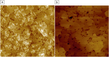
Despite large lattice mismatch (+19%), AlN buffer layers having smooth surface morphologies (typically with rms <0.5 nm) can be grown on Si(111). Typical surface morphologies of AlN buffer layers grown on Si(111) by metal–organic chemical vapor deposition (MOCVD)Reference Frayssinet, Cordier, Schenk and Bavard17 and molecular beam epitaxy (MBE)Reference Moreno18 are shown in Figure 1. It is worth noting that there is no issue regarding the control of the polarity of the AlN buffer layer, and only the Al-polarity (Al–N bond parallel to the growth axis is oriented from the Al atom toward the N atom) is obtained starting from a clean silicon surface. It is also worth noting that growth of GaN directly on Si is very challenging due to a reaction between Ga and Si (melt-back etching).Reference Zhu, Wallis and Humphreys9
Atomic force microscope images (1 μm × 1 μm) of the surface morphology of a 200-nm-thick AlN buffer layer grown on Si(111) by (a) NH3 molecular beam epitaxy (MBE)Reference Moreno18 at 1030°C and (b) metal–organic chemical vapor deposition (MOCVD) at 1145°C.Reference Frayssinet, Cordier, Schenk and Bavard17 Under optimized growth conditions, the roughness is about the same (≤0.5 nm), independent of the growth techniques used. Terraces and step-edges are resolved on surfaces grown by MBE, while dislocations and grain boundaries are observed on surfaces grown by MOCVD.

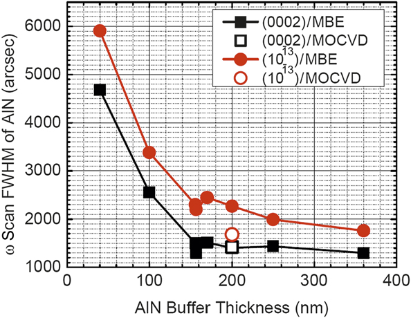
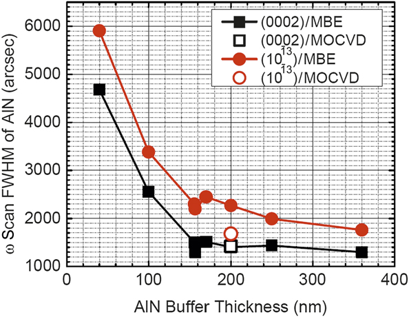
Other buffer layer materials have been proposed,Reference Zhu, Wallis and Humphreys9 such as SiC, boron monophosphide, and scandium nitride, but AlN buffer layers are by far the preferred choice because of easy implementation.Reference Zhu, Wallis and Humphreys9 As shown in Figure 2, the crystalline quality of AlN buffer layers improves with AlN thickness. When the growth conditions and cleaning of the Si surface are optimized, similar structural qualities are achieved using both MOCVD and MBE.Reference Frayssinet, Cordier, Schenk and Bavard17,Reference Moreno18 As studied on plan-view transmission electron microscopy images, the threading dislocation density (TDD) reaching the AlN surface ranges from high to low 1010 cm–2. As discussed in the next section, the surface morphology and crystalline quality of AlN influence the strain relaxation kinetics of the top GaN layer.
The dependence of full width at half maximum (FWHM) of AlN (002) and (103) x-ray diffraction ω scans on AlN buffer layer thickness grown by molecular beam epitaxy (MBE)Reference Moreno18 and metal–organic chemical vapor deposition (MOCVD).Reference Frayssinet, Cordier, Schenk and Bavard17 Under optimized growth conditions, the threading dislocation density (TDD) in AlN layers grown by MOCVD is in the low 1010 cm–2, while TDD values for NH3 MBE are in the high 1010 cm–2. The difference arises mainly because of the growth temperature.
AlN buffer layers are good candidates for the growth of GaN on Si, but it is important to mention that the nucleation of AlN on Si is a very complex process,Reference Semond, Cordier, Grandjean, Natali, Damilano, Vézian and Massies8,Reference Zhu, Wallis and Humphreys9,Reference Le Louarn, Vézian, Semond and Massies19,Reference Dadgar, Hempel, Bläsing, Schulz, Fritze, Christen and Krost20 and the formation of the AlN/Si interface raises many questions.Reference Kaiser, Jakob, Zweck, Gebhardt, Ambacher, Dimitrov, Schremer, Smart and Shealy7,Reference Zhu, Wallis and Humphreys9,Reference Le Louarn, Vézian, Semond and Massies19,Reference Liu, Ponce, Dadgar and Krost21–Reference Radtke, Couillard, Botton, Zhu and Humphreys23 Interestingly, it has recently been reported that the AlN/Si interface is likely responsible for a strong decrease in the device breakdown voltage,Reference Yacoub, Fahle, Finken, Hahn, Blumberg, Prost, Kalisch, Heuken and Vescan24 and by removing the Si substrate, it is possible to significantly enhance the breakdown voltage.Reference Srivastava, Das, Visalli, Derluyn, Van Hove, Malinowski, Marcon, Geens, Cheng, Degroote, Leys, Germain, Decoutere, Mertens and Borghs25 The following discussion will give a deeper insight into the complexities surrounding the AlN nucleation process on Si, which will subsequently enable us to answer how to obtain a sharp AlN/Si interface. With a sharp interface, the growth process is under control and reproducible.
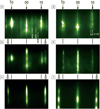
Using MBE,Reference Semond, Cordier, Grandjean, Natali, Damilano, Vézian and Massies8,Reference Le Louarn, Vézian, Semond and Massies19,Reference Nikishin, Antipov, Francoeur, Faleev, Seryogin, Elyukhin, Temkin, Prokofyeva, Holtz, Konkar and Zollner26 which requires an ultrahigh vacuum (UHV) and a clean environment, it has been shown that any residual traces of NH3 in the atmosphere surrounding a clean Si substrate will react with its surface (Figure 3a). Depending on the surface temperature and the amount of NH3 in the surroundings, SiNx species form at the surface of the substrate. They may take different forms, such as weakly bonded species, a very thin crystalline layer, or amorphous nanometer thick layers.
Reflection high-energy electron diffraction patterns along the [–110] azimuth of Si(111) during AlN nucleation. (a–c) NH3-first nucleation process: (a) after NH3 pre-flow of Si(111) at 650°C and rapid thermal annealing at 820°C, a (8 × 8) surface reconstruction characteristic of β-Si3N4(0001) surface is obtained. (b) After deposition of 1 monolayer (ML) of aluminum at 650°C, the AlN(0001) (1 × 1) orders indicated by white arrows coexist with the Si(111) ones and (c) after the growth of 40 nm AlN buffer layer at 920°C. (d–f) Al-first nucleation process: (d) after deposition of 1 ML of aluminum at 650°C leading to the formation of the Al-Si γ phase, (e) after the nitridation of the γ phase at 650°C, and (f) after the growth of 40 nm AlN buffer layer at 920°C. Reprinted with permission from Reference 19. © 2009 Elsevier.

Interestingly, whichever growth technique is used, MBE or MOCVD, sharp AlN/Si interfaces have been demonstratedReference Semond, Cordier, Grandjean, Natali, Damilano, Vézian and Massies8,Reference Liu, Ponce, Dadgar and Krost21 using very different and sometimes opposite growth strategies. Some MOCVD researchersReference Zhu, Wallis and Humphreys9,Reference Dadgar, Hempel, Bläsing, Schulz, Fritze, Christen and Krost20,Reference Yacoub, Fahle, Finken, Hahn, Blumberg, Prost, Kalisch, Heuken and Vescan24 do not remove the oxide layer from the starting Si surface, more likely considering that it is a protective layer against species in the growth chamber. Once the desired temperature is reached (above the temperature required to remove the oxide), the surface is first exposed to a trimethylaluminum (TMA) pre-dose, which is key to obtain a sharp AlN/Si interface. Other MOCVD researchers expose the clean Si surface to an NH3 pre-flow before starting the AlN buffer layer growth. Some researchers have observed that there is always a SiNx amorphous interlayer at the AlN/Si interface.Reference Zhu, Wallis and Humphreys9 More or less, the same statement can be applied to MBE, with some researchers suggesting that it is essential to use an Al pre-dose (Figure 3d), and others reporting that an NH3 pre-flow (Figure 3a) is key to getting a sharp interface.
Is there a rational explanation for these contradictory observations? When a Si surface is exposed to TMA or Al, the Al atoms have a strong tendency to diffuse into the Si (especially considering the very high temperature, 900–1200°C, used for AlN growth),Reference Wen, Dähne-Prietsch, Bauer, Cuberes, Manke and Kaindl27,Reference Calleja, Sánchez-García, Basak, Sánchez, Calle, Youinou, Muñoz, Serrano, Blanco, Villar, Laine, Oila, Saarinen, Hautojärvi, Molloy, Somerford and Harrison28 and an Al-Si alloy may form (Figure 3d).Reference Gröger and von Blanckenhagen29,Reference Saranin, Kotlyar, Zotov, Kasyanova, Cherevik and Lifshits30 Knowing this, it is hard to explain how a TMA or Al pre-flow would help give a sharp AlN/Si interface. However, one possible explanation is that a thin SiNx layer is unintentionally formed, right after the oxide removal, and when Al atoms reach the surface, they weaken the Si–N bonds and form Al–N bonds (Figure 3b), which are energetically more favorable. Of course, this would happen only if the SiNx layer is very thin, typically a monolayer. This scenario is supported by studies carried out for MBE showing that even in a UHV growth reactor, any residual background traces of NH3 surrounding a clean Si surface will form a very thin crystalline SiNx layer, even at low temperatures (Figure 3a).Reference Semond, Cordier, Grandjean, Natali, Damilano, Vézian and Massies8,Reference Le Louarn, Vézian, Semond and Massies19,Reference Nikishin, Antipov, Francoeur, Faleev, Seryogin, Elyukhin, Temkin, Prokofyeva, Holtz, Konkar and Zollner26 These studies also show that such a very thin crystalline SiNx layer can be reduced using an Al pre-dose leading to the formation of epitaxial AlN islands (Figure 3b) because of the more energetically favorable Al–N bond versus the Si–N bond.
This also explains why exposing the Si surface to a well-controlled small amount of NH3 right after the oxide removal could lead to a sharp AlN/Si interface. Therefore, it seems that the choice of Al-first or NH3-first is related to the cleanliness (mostly related to the unwanted NH3 residual background pressure) inside the growth reactor. The nucleation temperature also plays a key role; the lower the temperature, the lower the probability of forming an amorphous interlayer. Note that whatever growth temperature is used, a crystalline SiN monolayer will form as soon as some ammonia reaches the Si surface. At low temperatures there is not enough energy for the NH molecules to diffuse through the crystalline SiN layer to form a thick amorphous SiN layer.
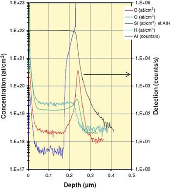
It is also important to remember that from a crystallographic point of view, a sharp interface (where there is no amorphous interlayer) does not necessarily mean that the interface is sharp from a chemical point of view. During growth of AlN buffer layers on Si, the Si atoms out-diffuse from the substrate into the growing layer, and Al atoms may diffuse into the Si substrate as well. Figure 4,Reference Moreno18 which corresponds to the NH3-first nucleation process shown in Figure 3a–c, presents secondary ion mass spectrometry profiles measured from an AlN buffer layer (250 nm thick) grown by MBE on Si(111). The AlN nucleation was carried out at 650°C, followed by a temperature ramp above 900°C to promote AlN growth. Despite this rather low growth temperature, Si and Al diffusion across the interface was visible. Beyond a depth of a few tens of nanometers depth, the Si atom concentration in AlN decreased abruptly, reaching a background level in the mid-1017 atoms/cm3. On the other hand, despite the use of the NH3 pre-flow nucleation process shown in Figure 3a–c, Al diffusion into the silicon is observed, resulting in an Al-doped silicon subsurface layer. One could anticipate that Al diffusion would be even higher using a TMA or Al pre-flow nucleation process. The residual carbon and oxygen concentration in the AlN buffer layer, respectively, was about 2 × 10¹⁸ and 2 × 10¹⁹ atoms/cm3 and is likely from the growth chamber. The amount of carbon and oxygen atoms at the AlN/Si interface turns out to be highly dependent on the cleaning procedure used for the silicon wafers (ex situ versus in situ, low temperature versus high temperature).Reference Moreno18
Secondary ion mass spectrometry results for a 250-nm-thick AlN buffer layer grown by NH3 molecular beam epitaxy at 920°C.Reference Moreno18 AlN nucleation is made using the NH3 first nucleation process, as shown in Figure 3a–c.

Thus, nucleation of AlN on Si is a critical step, and some companies are now developing growth reactors with in situ chamber cleaning procedures in order to specifically address this cleanliness issue. However, despite the importance of this step and the very well-known related issues, there are few reports on fabrication of devices using GaN on Si that discuss this aspect. This is surprising, because in terms of reproducibility, performance, and reliability, the nucleation process is critical.
GaN growth for electronic applications
In order to obtain low TDD GaN on Si, a 3D growth mode is required, where growth conditions reduce the density of dislocations reaching the top surface, thus achieving a TDD as low as few 108 cm–2 can be achieved.Reference Zhu, Wallis and Humphreys9 This is typically what is needed to fabricate high-efficiency LEDs. Unfortunately, for the fabrication of AlGaN/GaN high-electron-mobility transistors (HEMTs), such a 3D growth mode is prohibited. As a result, GaN on Si layers developed for electronic devices have a higher TDD, typically 109 cm–2 or higher.
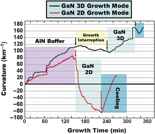
There are several reasons why a 3D growth mode cannot be applied for HEMTs for growing GaN: Three-dimensional growth of GaN is accompanied by impurity incorporation (mainly oxygen) (Figure 5), resulting in a conductive GaN layer, while for electronic devices, highly resistive GaN layers are mandatory. In addition, the most popular technique to promote 3D growth is to use a SiN masking layer, and it is suspected that Si atoms form a doped layer that is not desiredReference Dadgar, Hempel, Bläsing, Schulz, Fritze, Christen and Krost20 for highly resistive layers.
In situ wafer curvature measured during the growth by NH3 molecular beam epitaxy of a 500-nm-thick GaN layer on a 200-nm-thick AlN buffer layer on 2-in (∼50 mm) Si(111) substrates. Red curve: GaN layer following a 2D growth mode on the AlN buffer layer; a compressive strain develops. Black curve: After a growth interruption that is required for the deposition of a SiN masking layer, GaN grows following a 3D growth mode (as indicated by the reflection high-energy electron diffraction pattern). A tensile strain develops due to strain relaxation, followed by the coalescence of islands.
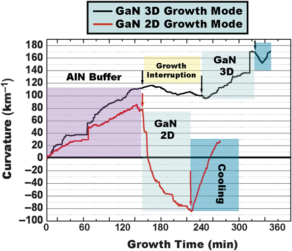
Three-dimensional growth of GaN allows fast relaxation of epitaxial strain, which is not desirable and leads to cracking of the GaN epilayer. To grow crack-free GaN layers on Si, it is necessary to maintain a certain amount of compressive strain in GaN in order to compensate for the tensile strain appearing during the post-growth cooling from the growth temperature to room temperature (Figure 5). This tensile strain is due to the larger thermal expansion coefficient (115%) of GaN with respect to Si. To maintain the GaN layer under compressive strain, the GaN layer must be grown on a layer having a smaller in-plane lattice parameter such as AlN or AlGaN.Reference Zhu, Wallis and Humphreys9,Reference Baron, Cordier, Chenot, Vennéguès, Tottereau, Leroux, Semond and Massies31 By increasing the layer thickness, strain relaxation occurs, and the GaN layer tends to recover its fully relaxed in-plane lattice parameter, which leads to cracking during cooling. At this point, the know-how of the growers comes into play to find ways of slowing down the relaxation rate of the growing GaN layer.Reference Baron, Cordier, Chenot, Vennéguès, Tottereau, Leroux, Semond and Massies31 In order to slow down the strain relaxation kinetics during growth of GaN on an Al-containing layer, the growth mode must be as close to 2D as possibleReference Baron, Cordier, Chenot, Vennéguès, Tottereau, Leroux, Semond and Massies31 (i.e., the growth front should be as smooth as possible). As soon as growth conditions (temperature, V/III ratio or amount of ammonia to the amount of Ga) deviate from a perfect 2D growth mode, the strain relaxation kinetics are enhanced. Consequently, to prevent cracking, growth of GaN must be 2D, which also means that the surface morphology of the initial AlN or AlGaN buffer layer needs to be as smooth as possible. Interestingly, TDD plays an important role in the strain relaxation kinetics.Reference Langer, Barski, Barbier, Renaud, Leszczynski, Grzegory and Porowski32 A lower TDD results in slower strain relaxation kinetics.
It is still an open question as to whether low/ultralow TDD (1–9 × 108 cm–2 and < 1 × 108 cm–2, respectively) GaN layers (unintentionally doped) are desirable, as it seems they are generally not resistive. In this application, it is important to reduce the leakage current as much as possible, thus low conductivity is desirable. It has been shown that some dislocations could act as acceptors, and they are very efficient in preventing leakage in GaN layers, resulting in lower buffer conductivity. Also, negatively charged dislocations may act as scattering centers, thus further reducing the buffer conductivity.
Because AlGaN/GaN HEMTs are grown using the 2D growth mode, the TDD typically ranges from 109 to 1010 cm–2, depending mostly on the overall thickness of layers. Despite such a high TDD, 2D electron gas mobility values of 2000 cm2/V∙s, which are close to the theoretical limit, are achieved with a sheet carrier concentration of approximately 1 × 1013 cm–2.Reference Baron, Cordier, Chenot, Vennéguès, Tottereau, Leroux, Semond and Massies31,Reference Cheng, Liang, Van Hove, Geens, De Jaeger, Srivastava, Kang, Favia, Bender, Decoutere, Dekoster, del Agua Borniquel, Jun and Chung33 Then, using the basic ideas discussed previously about Si out-diffusion, Al-diffusion, Ga-diffusion (responsible for the so-called melt-back etching but not discussed in this article), impurity incorporation, strain relaxation kinetics, TDD, and complex interplay among these phenomena, growers have developed many more sophisticated heterostructures.Reference Srivastava, Das, Visalli, Derluyn, Van Hove, Malinowski, Marcon, Geens, Cheng, Degroote, Leys, Germain, Decoutere, Mertens and Borghs25,Reference Baron, Cordier, Chenot, Vennéguès, Tottereau, Leroux, Semond and Massies31,Reference Cheng, Liang, Van Hove, Geens, De Jaeger, Srivastava, Kang, Favia, Bender, Decoutere, Dekoster, del Agua Borniquel, Jun and Chung33–Reference Selvaraj, Selvaraj and Egawa35
To improve material properties and/or device performances, growers may decide to use AlGaN buffer layers above the first AlN buffer layer, and carbon-doping of GaN to increase buffer resistivity may also be implemented, as well as the use of superlattices or AlGaN/AlGaN multiple interfaces. However, despite promising device performances, AlGaN/GaN heterostructures on Si still contain imperfections (dislocations, strain), which may lead to premature failure and reliability problems.Reference Wuerfl, Bahat-Treidel, Brunner, Cho, Hilt, Ivo, Knauer, Kurpas, Lossy, Schulz, Singwald, Weyers and Zhytnytska16 So, what can be done to improve performance, reproducibility, and reliability from the growth side? There is little evidence that dislocations are a first-order problem, but one can anticipate that reduction of the TDD is going to be essential. It could be that next-generation GaN on Si for power electronics will be grown using the 3D instead of 2D growth mode, taking advantage of developments for LEDs. At the same time, solutions need to be proposed to fabricate highly resistive, low TDD buffer layers. In addition, recent results showing the achievement of high breakdown voltage using thin epilayersReference Srivastava, Cheng, Das, Van Hove, Leys, Marcon, Visalli, Geens, Decoutere, Mertens and Borghs36 suggest this could be an interesting approach in simplifying growth processes to reduce bowing/cracking issues and to lower cost.
Despite the presence of imperfections, promising results have been reported using GaN on Si for power electronics. Now, we must address reproducibility and reliability issues. Some of these issues are likely to be related to growth processes and/or material imperfections. In the last few years, GaN on Si has been engaged in a very competitive race with GaN on Al2O3 for LEDs, and the grower’s toolbox for GaN on Si has been significantly improvedReference Zhu, Wallis and Humphreys9 and may lead to future improvements for power electronics, likely centered on materials quality and simplified heterostructures.
Conclusions
This article presents some of the challenges of epitaxial growth of GaN on Si related to the fabrication of AlGaN/GaN heterostructures for power electronics applications. Nucleation of the AlN buffer layer on Si is discussed, and an explanation is given in order to understand the different optimization processes that are reported. If nucleation is not well understood or well controlled, it could result in poor reproducibility. Moreover, supported by recent studies on the influence of the AlN/Si interface on the breakdown voltage, it is likely that the nucleation process is also responsible for device performance and reliability. Through the choice of using a 2D growth mode for AlGaN/GaN HEMTs instead of a 3D growth mode, basics of the growth of GaN on Si are reviewed. It is anticipated that material imperfections, such as dislocations and strain, could be considered as sources of device degradation; the epitaxial challenges discussed in this article should be fully understood and well controlled for the fabrication of high-performance, reproducible, and reliable AlGaN/GaN HEMTs on silicon.
Acknowledgments
The author thanks J.C. Moreno, A. Le Louarn, S. Vézian, and M.J. Rashid for assistance in the growth experiments, and E. Frayssinet, Y. Cordier, P. Srivastava, and S. Rennesson for fruitful discussions.