Introduction
In recent years, network communications around the world have been steadily developing towards high-speed communications and wide bandwidth. As people rely on fifth-generation (5G) communication technology and millimeter wave(mm-Wave) has attracted much attention in current 5G and future 6G wireless communications [Reference Qin, Chen and Xiang1–Reference Chung, Lee, Hsu and Lin4]. However, the mm-Wave has very high losses when using microstrip line circuits. Therefore, under the requirements of low loss, high-quality transmission, and high power, using substrate integrated waveguide (SIW) for circuit design has become a better choice [Reference Ashraf, Sebak and Kishk5–Reference Sun, Ban, Che and Nie10]. To achieve multi-beam control, beamforming networks have been widely used in 5G communications [Reference Li, Wu, Cao, Chen, Li and Zhang11, Reference Klionovski, Sharawi and Shamim12]. In recent years, the combined application of the Butler matrix and the array antenna has attracted much attention [Reference Xu, Shen, Xue and Hu13, Reference Aribi, Sedghi and Lou14]. The reason is that the Butler matrix has smooth transmission performance and modular component configuration. Therefore, applying the Butler matrix to the mm-Wave can provide a wider spectrum and lower delay transmission rate [Reference Liu, Chen and Qin15].
Common matrices currently include the Nolen matrix, Blass matrix, and Butler matrix. The Blass matrix requires the use of a fixed coupler for a larger range of coupling to achieve a good waveguide directional coupler, but its size advantage is not as good as the Nolen matrix and Butler matrix [Reference Lialios, Zekios and Georgakopoulos16]. The Nolen matrix [Reference Yang, Pan, Zheng, Hong and Chan17] is more flexible to design any number of beams, and the circuit paths do not need to be crossed. However, the Nolen matrix requires more couplers to design, so the circuit will be more complex than the Butler matrix. The Butler matrix also has many applications in radar, military, and satellites due to its relatively simple design [Reference Hilario Re, Comite, Podilchak, Alistarh, Goussetis, Sellathurai, Thompson and Lee18–Reference Agrawal and Kumar20]. In Zhong et al. [Reference Zhong, Ban, Lian, Yang, Guo and Yu21], the Butler matrix is mentioned to have better performance and ease of design, and can provide higher beam resolution from different feed designs.
Beamforming networks based on SIW structures can reduce transmission losses and are easily integrated and designed on planar structures [Reference Sun, Ban, Lian, Liu and Nie22, Reference Idury, Delmonte, Silvestri, Bozzi and Mukherjee23]. In recent years, many studies on Rotman lenses have also introduced SIW structures for design. The Rotman lens is a beamforming network that does not depend on the active circuit. The simple structure, wide bandwidth, and high gain characteristics of Rotman lenses have become one of the options for mm-Wave imaging applications [Reference Eid, Hester and Tentzeris24]. However, due to the high coupling characteristics of the Rotman lens between adjacent connection terminals, the connection terminals will easily interact with each other and reduce efficiency [Reference Li, Wu, Cao, Chen, Li and Zhang11]. On the other hand, the symmetrical structure of the Butler matrix can provide equal power distribution, and through this characteristic, better matching and isolation performance can be achieved [Reference Kong, Hu, Li, Zhang and Hong25].
Due to the unique performance of Butler matrices in millimeter waves, there are more and more studies on the combination of Butler matrices and array antennas. A 5 × 8 Butler matrix applied to the mm-Wave is designed in Qin et al. [Reference Qin, Chen and Xiang1]. To simplify the number and complexity of intersections in the matrix structure, a double-layer symmetrical SIW structure is used to design the Butler matrix. A S-band 8 × 8 Butler matrix is proposed in Wincza et al. [Reference Wincza, Gruszczynski and Sachse26]. The Butler matrix adopts a microstrip design and reduces the overall size through the modular component configuration of the Butler matrix. However, the radiation loss of the microstrip line structure is higher in the mm-Wave. In refs [Reference Yan, Zhao, Ban, Lian and Nie27, Reference Lian, Ban, Zhu and Guo28], a multi-beam feed circuit is also designed through a double-layer SIW structure to reduce the side lobe level (SLL). These studies show that in millimeter-wave designs, the Butler matrix of the SIW structure has better transmission performance than the Butler matrix of the microstrip structure. Many Butler matrix researches often choose slot antennas and patch antennas that are simple in structure and easy to integrate when designing mm-Wave multi-beam array antennas [Reference Qin, Chen and Xiang1, Reference Sun, Ban, Lian, Liu and Nie22, Reference Wu, Zhang, Zhou and Huang29–Reference Shady and Kishk37]. In Wu et al. [Reference Wu, Zhang, Zhou and Huang29], the three-layer 7 × 8 Butler matrix with an SIW slot array antenna effectively reduces the Butler matrix’s size. In Yang et al. [Reference Yang, Gao, Luo, Wen, Ban, Ren, Wu, Yang and Liu30], a patch antenna was used to design a multi-beam array antenna for the mm-Wave. The above two documents show that the patch array antenna has relatively good beam control performance. In Chung et al. [Reference Chung, Lin and Yang36], a Butler matrix patch antenna with microstrip line structure was proposed applied in 28 GHz. The beam angle generated by this antenna using a patch antenna can be better close to the ideal angle.
Therefore, this paper proposes a mm-Wave 4 × 4 Butler wide bandwidth patch antenna based on a planar SIW architecture. This design combines Butler matrix and patch array antennas to achieve a multi-beam switching wide bandwidth antenna with high-wide bandwidth, high gain, and precise beam angle. The proposed Butler matrix removes the 0° phase shifter in the conventional 4 × 4 Butler matrix and only configures two 45° phase shifters to achieve ±15° and ±45° beam ranges. At the same time, the antenna has the characteristics of a low side lobe level and can maintain good transmission quality. The antenna is integrated into a single-layer planar substrate and can be produced in a simple and low-cost manner.
Design structure of the Butler matrix
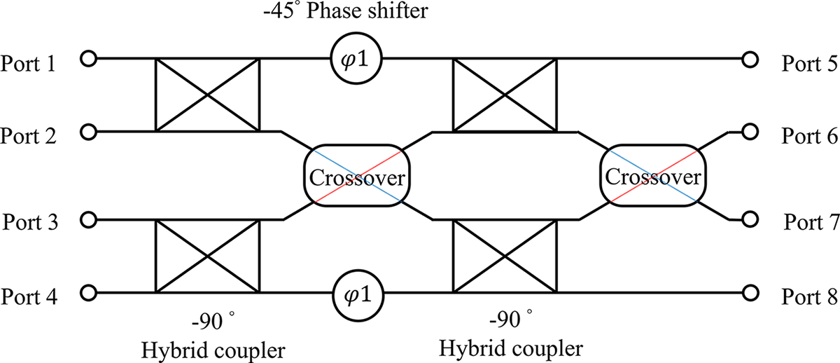
The traditional 4 × 4 Butler matrix design contains 4 inputs and 4 outputs. When the Butler matrix excites the inputs, each input will provide a different output beam. Figure 1 is the 4 × 4 Butler matrix circuit configuration, including four −90° hybrid couplers, two cross-classifiers and two −45° phase shifters. As can be seen in Fig. 1, the Butler matrix in this article only needs to use two −45° phase shifters to produce beam angles close to −45°, 135°, −135°, and 45°. In the Butler matrix, port 1 is the input end, port 2 is the isolation end, port 3 is the output end, and the coupling end of port 4. The cross-classifier is composed of two hybrid couplers based on the design characteristics of the SIW structure. To reduce the cross-coupler transmission loss, the central vertical interconnect access (VIA) design is adjusted so that the loss is close to 0 dB. The phase shifter uses the curvature of the delay line to accurately design the phase at −45°. The Butler matrix design was simulated using a Rogers Duroid 5880 substrate with a loss tangent of 0.0009 and a relative dielectric constant of 2.2.
Butler matrix architecture.

Hybrid coupler design
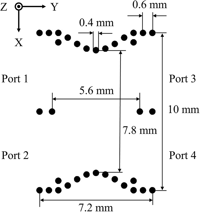
Hybrid couplers utilize the extended design of the Riblet structure [Reference Tiwari and Rao38, Reference Kim, Hirokawa and Ando39], which provides uniform power distribution, isolation, and matching effects. Through SIW technology, the common wall can be eliminated, and the design can produce electrical characteristics like that of a rectangular waveguide. The hybrid coupler designed in this article uses a VIA with a diameter of 0.4 mm and a VIA spacing of 0.6 mm, as shown in Fig. 2. The spacing and diameter between VIAs are designed according to the rules mentioned in Aourik et al. [Reference Aourik, Errkik, Zbitou and Latrach35] to minimize the radiation loss of the electric field. According to (1) [Reference Iqbal, Tiang, Wong, Alibakhshikenari, Falcone and Limiti40], the effective waveguide width can be derived to determine better support for the transverse electric field (TE) mode in the 38 GHz frequency range. Where  ${\omega _{eff}}$ is the effective width of the waveguide,
 $\omega $ is the width of the SIW,
 $d = 2r$ is the diameter of the VIA (
 $r$ is the radius), and
 $p$ is the spacing between the through holes. In the structural design, the upper and lower rows of VIA are arranged in a curved manner, making the structure approximate to two transverse waveguides. In Fig. 3(a), S11 can cover 28–41 GHz at −10 dB, the isolation S21 is close to −38 dB, and the output losses of both S31 and S41 are about 3 dB. Figure 3(b) shows that the signal output phase difference is −90°, so the coupler is also called a 3 dB −90° hybrid coupler.
 \begin{equation}\begin{array}{*{20}{c}}
{{\omega _{eff}} = \omega - 1.08\frac{{{d^2}}}{p} + 0.1\frac{{{d^2}}}{\omega }}
\end{array}\end{equation}
Hybrid coupler structure.

Simulation results of hybrid coupler. (a) S-parameters. (b) Phase.

Crossover design
The SIW crossover is a combination of two hybrid couplers, as shown in Fig. 4(a). Port 1 in the crossover is connected to port 4 and port 2 to port 3. The transmission loss S41 at 38 GHz is almost close to 0 dB, as shown in Fig. 4(b). During the evolution of Crossover, the VIAs in the center of the upper and lower rows are simplified and connected with straight lines, as shown in Fig. 5(a). To make the transmission loss closer to 0 dB, two VIAs are added in the center, and the relationship between the spacing of the two VIAs and the loss is analyzed. Finally, the best transmission loss is obtained when the distance between the two central VIAs is 1.2 mm, as shown in Fig. 5(b).
Structural design and simulation results of crossover. (a) Crossover structure. (b) S-parameter simulation results.

Evolution analysis of crossover. (a) Three structures. (b) Transmission loss.

Phase-shifter design
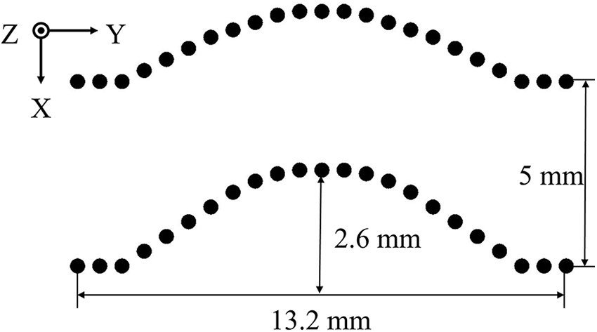
In the Butler matrix, a fixed output phase can be achieved through the phase angle of the phase shifter and the phase difference of the hybrid coupler. The delay line structure is the simplest way to design a phase shifter. From (2), the SIW delay line phase shifter can control the phase delay through the length and shape of the waveguide. In the formula, λ is the wavelength in the waveguide, and l is the delay line length. This design allows precise phase control without increasing the overall size. The phase shifter in this article realizes a −45° phase shifter through a curved SIW transmission line, and the dimensions are shown in Fig.6. The curvature of the transmission line allows the phase of the phase shifter to be accurately controlled at −45.13° and provides good wide bandwidth signal transmission, as shown in Fig. 7.
 \begin{equation}\begin{array}{*{20}{c}}
{\Delta \Phi = \frac{{2\pi }}{{\lambda g}} \cdot l}
\end{array}\end{equation}
−45° Delay line phase-shifter structure.

Simulation results of −45° phase shifter. (a) S-parameters. (b) Phase.

Butler matrix structure and performance
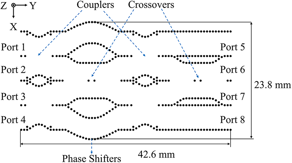
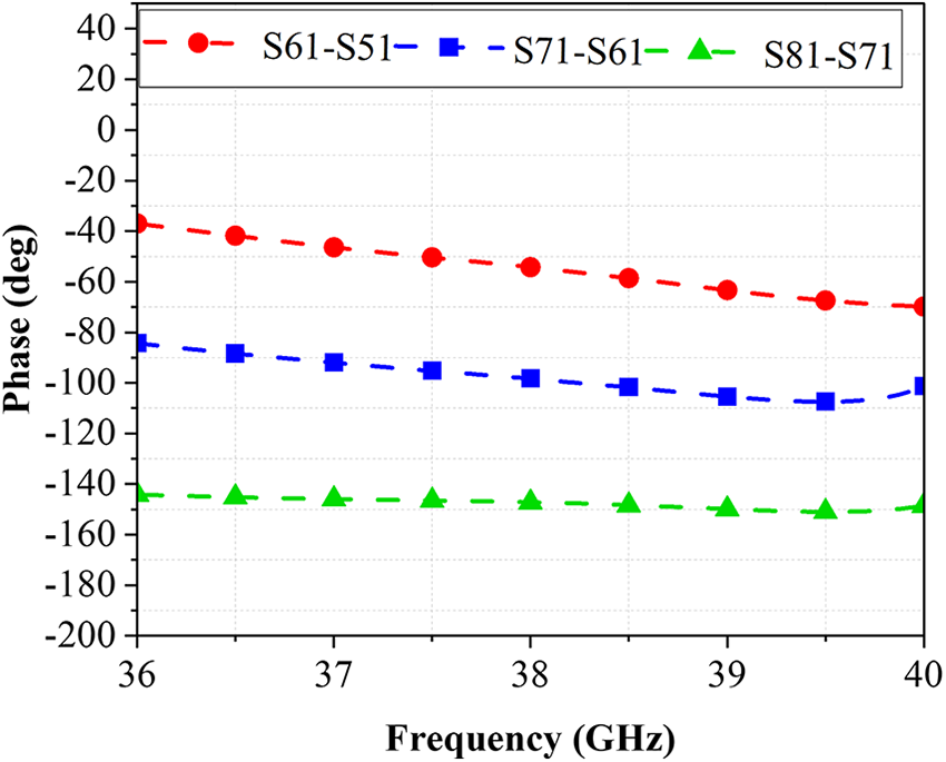
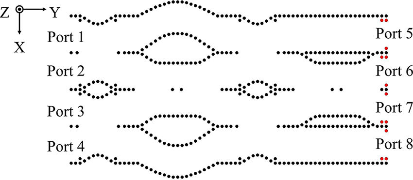
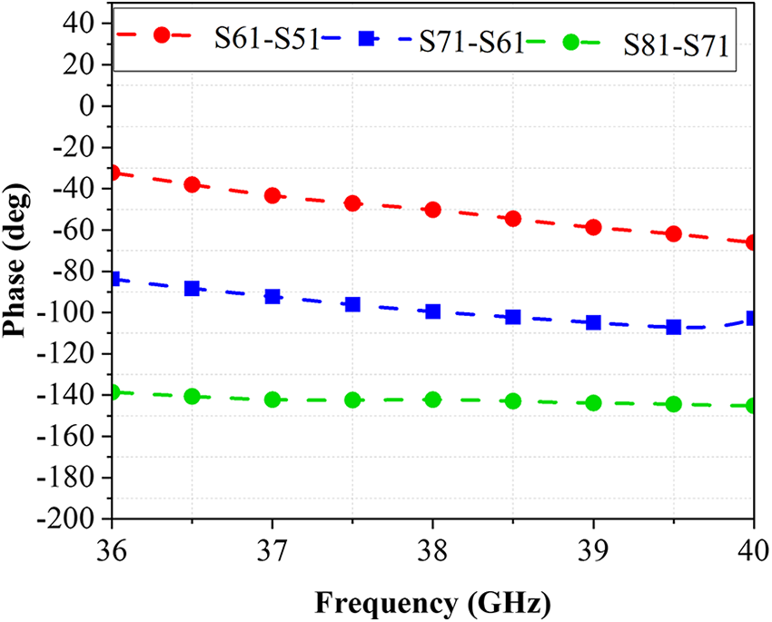
The Butler matrix in this article is a combination of the hybrid coupler, cross coupler, and phase shifter designed in the previous chapters. The configuration and size of the Butler matrix are shown in Fig. 8. Each component is connected to the first VIA and the last VIA with a gap of 0.6 mm and is simulated and verified using electromagnetic simulation software. Figure 8 shows that the Butler matrix is a symmetric structure, so port 1 and port 4, port 2 and port 3 are all symmetrical relationships. In Fig. 9, the S-parameter of the Butler matrix can cover 34–40.3 GHz (bandwidth 16.9%) under the standard below −10 dB. The simulation results of port 1 and port 4 and port 2 and port 3 are almost the same. In Fig. 10, when port 1 is excited, the phase difference between port 5 and port 6, port 7 and port 8 does not reach the ideal phase difference (−45°, −90°, and −135°). To make the phase closer to the ideal phase difference, VIA is added to ports 5–8 to affect the impedance matching, as shown in Fig. 11. In Fig. 12, the adjusted Butler matrix bandwidth covers 33.9–40.3 GHz (bandwidth 17.2%). In Fig. 13, the output phase difference after exciting port 1 is also closer to the ideal phase difference of −45, −90, and −135°.
Configuration of the Butler matrix structure.

S-parameter simulation results of the Butler matrix.

The output phase difference of the Butler matrix when port 1 is excited.

Configuration of the adjusted Butler matrix.

S-parameter simulation results of the adjusted Butler matrix.

The adjusted Butler matrix excites the output phase difference of port 1.

Patch antenna design and configuration for beam switching
Design of patch antenna
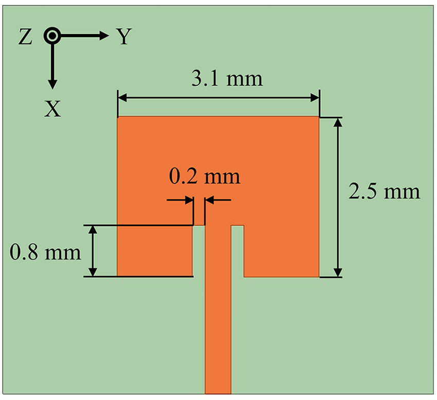
The patch antenna can enhance the bandwidth and beamforming capabilities of the Butler matrix while maintaining the uneven amplitude of the phase difference. Patch antennas provide good radiation patterns in high-frequency applications at low manufacturing costs. Figure 14 shows the patch antenna structure applied to the Butler matrix in this article. The patch antenna structure can be designed and calculated using (3)–(6) [Reference Chung, Lin and Yang36]. Where  ${v_C}$ is the speed of light, the length is L, the width is W, and the thickness is h. Figure 15 shows the simulated S-parameters and radiation pattern of a single patch antenna. In Fig. 15(a), the single patch antenna can cover the bandwidth of 37.3–38.6 GHz under the −10 dB standard and the return loss at 38 GHz is close to −33 dB. The peak gain of a single patch antenna is 7.6 dBi, as shown in Fig. 15(b).
 \begin{equation}\begin{array}{*{20}{c}}
{{f_C} = \frac{{{v_c}}}{{2{L_{eff\sqrt {{\varepsilon _{eff}}} }}}} = \frac{1}{{2\left( {L + 2{{\Delta }}L} \right)\sqrt {{\varepsilon _{eff}}} \sqrt {{\mu _0}{\varepsilon _0}} }} = q\frac{{{v_c}}}{{2L\sqrt {{\varepsilon _0}} }}}
\end{array}\end{equation}
 \begin{equation}\begin{array}{*{20}{c}}
{{\varepsilon _{eff}} = \frac{{{\varepsilon _r} + 1}}{2} + \frac{{{\varepsilon _r} - 1}}{2}\frac{1}{{\sqrt {1 + \frac{{12w}}{h}} }}}
\end{array}\end{equation}
 \begin{equation}\begin{array}{*{20}{c}}
{W = \frac{1}{{2{f_{rc}}\sqrt {{\varepsilon _{eff}}} \sqrt {{\mu _0}{\varepsilon _0}} }}\sqrt {1 + \frac{2}{{{\varepsilon _r} + 1}}} = \frac{{{v_c}}}{{2{f_r}}}\sqrt {\frac{2}{{{\varepsilon _r} + 1}}} }
\end{array}\end{equation}
 \begin{equation}\begin{array}{*{20}{c}}
{L = \frac{1}{{2{f_{rc}}\sqrt {{\varepsilon _{eff}}} \sqrt {{\mu _0}{\varepsilon _0}} }} - 2\Delta L}
\end{array}\end{equation}
Structural dimension diagram of a single patch antenna.

Simulation result of the single patch antenna. (a) S-parameters. (b) 38 GHz radiation pattern.

Configuration of patch antenna array
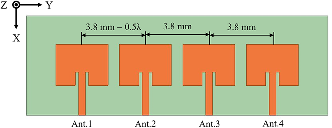
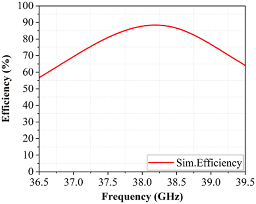
Figure 16 is a 38 GHz patch array antenna configuration. Each adjacent antenna is one-half wavelength apart from 38 GHz to effectively aggregate electromagnetic waves and increase antenna gain. Figure 17(a) shows that simultaneous excitation of Ant.1-4 can cover 37.4–38.8, 37.6–38.9, 37.6–38.9 and 37.4–38.8 GHz, respectively. At the same time, Fig. 17(b) also shows that the isolation between all antennas is below −10 dB. In addition, the beam gain of Ant.1-4 becomes 12.2 dBi, which is an overall increase of 4.6 dBi, as shown in Fig. 17(c). The array antenna has a more concentrated radiation beam, which means the antenna has good transmission quality. Finally, in Fig. 18, the antenna’s efficiency in the effective frequency band is 78.8–79.1%, and the efficiency at 38 GHz is 87.7%.
Patch array antenna structure and dimensions.

Simulation result of patch array antenna. (a) S-parameters. (b) Isolation. (c) 38 GHz radiation pattern.

Simulation efficiency of the patch array antenna.

Measurement and analysis discussion
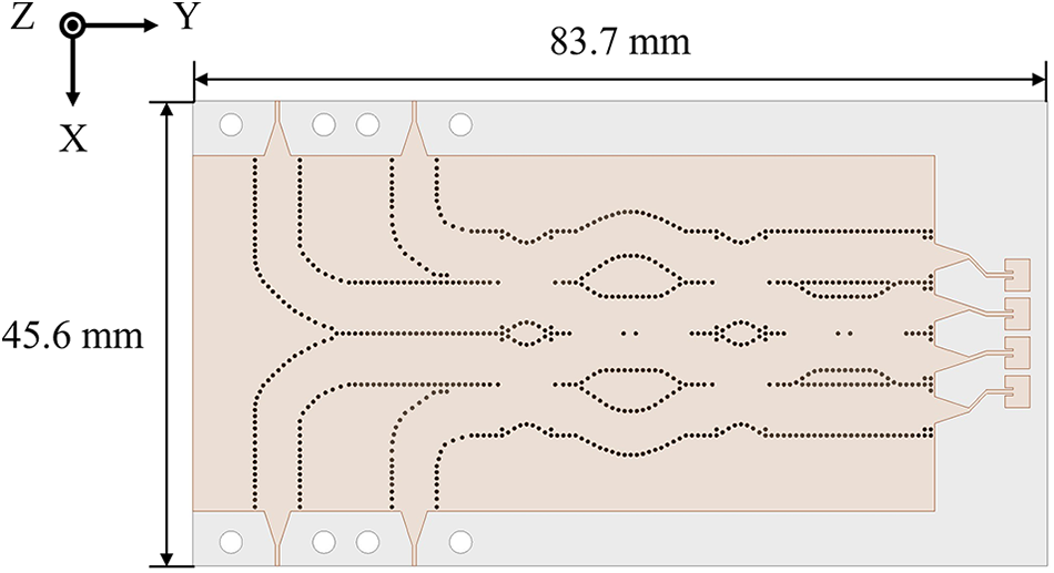
Figure 19 shows the structure and size of the combination of the Butler matrix and the patch antenna. The Butler matrix in this article needs to match the 50-Ohm SIW architecture with the 50-Ohm microstrip line. To achieve a complete matching effect between the Butler matrix and the patch array antenna, the transition structure of the microstrip taper needs to be added between the SIW and the microstrip line, as shown in Fig. 20. In single-layer circuits, microstrip taper is a common type of transition structure [Reference Kordiboroujeni and Bornemann41]. This transition structure provides good return loss over the full waveguide bandwidth. Figure 21(a) shows that the 4 × 4 Butler-wide bandwidth patch antenna is mainly divided into a conductor layer and a substrate layer. Finally, connect the end launch coaxial connector to the Butler matrix, as shown in Fig. 21(b). To reduce connection loss, the same microstrip taper transition structure is also added between the Butler matrix and the End Launch coaxial connector to achieve better match results.
4 × 4 Butler wide bandwidth patch antenna architecture.

SIW to microstrip transition structure.

Schematic diagram of the overall architecture of the 4 × 4 Butler-wide bandwidth patch antenna. (a) 3D-layered view. (b) Schematic diagram of adding the end launch coaxial connector.

The antenna is fabricated on a Rogers 5880 substrate with a thickness of 0.254 mm and a size of 83.7 × 45.6 mm2 (10.6λ0 × 5.77λ0), as shown in Fig. 22. Beamforming mainly uses the four patch antennas on the upper layer as the main radiation sources. The equipment used to measure the reflection coefficient is an Agilent network analyzer (model N5227A), which supports the 10 MHz to 67 GHz frequency band. The coaxial cable connected to the Butler matrix is WCA205-1.2 M to 65 GHz, with a total length of 120 mm, and its maximum supported frequency is 65 GHz. This cable is calibrated using SOL (short circuit, open circuit, load) and then the measurement is started, as shown in Fig. 23.
Prototype of 4 × 4 Butler-wide bandwidth patch antenna. (a) Top surface. (b) Bottom surface.

4 × 4 Butler wide bandwidth patch antenna for reflection coefficient measurement. (a) Erection method. (b) Antenna to be tested.

S-parameter analysis
Figure 24 shows the simulation and measurement results of the reflection coefficients (S11, S22, S33, S44) of the 4 × 4 Butler wide bandwidth patch antenna. In Table 1, the S-parameter simulation results of ports 1–4 can cover 33–42 GHz simultaneously, and the measured bandwidth is also consistent with the simulation, confirming that the antenna has a wide bandwidth advantage of close to 24%. Although the simulation and measurement results are slightly different, they almost maintain the same trend. These measurement differences may be due to loss in the end transmitter connector or manufacturing tolerances.
Reflection coefficient simulation and measurement results of the 4 × 4 Butler-wide bandwidth patch antenna ports 1–4. (a) Port 1. (b) Port 2. (c) Port 3. (d) Port 4. (e) Ports 1–4 measurement results.

Simulation and measurement of ports 1–4 reflection coefficient (s11–s44)

2D radiation direction analysis
In this article, mm-Wave chamber MW6 is used for radiation pattern measurement. The device environment can cover the range of 24–42 GHz. The measured antenna center point configuration can be seen in Fig. 25(a).
In Ma et al. [Reference Ma, Wu and Wang42], it is mentioned that the radiation pattern of an array antenna can be described by the array factor (AF), which is defined by (7). When different ports of the 4 × 4 Butler matrix are excited, the phase difference between adjacent output ports can be obtained by (8). According to the Butler matrix’s phase shift design, the corresponding phase values when Ports 1–4 are excited are shown in (9). Finally, the antenna radiation direction can be calculated by (10). Where In is the excitation vibration of the nth antenna unit,  ${\psi _{{\text{m}},{\text{m}} + 1}}$ is the phase difference between the m and m + 1 outputs,
 ${\psi _{0,1}} = 0$ is the reference phase, and
 ${d_{\text{r}}} = 2\pi d/\lambda $ is the ratio of the antenna spacing to the wavelength. Therefore, when Ports 1–4 are excited, the calculated main beam angles are approximately ±15° and ±45°.
 \begin{equation}\begin{array}{*{20}{c}}
{S\left( \theta \right) = \mathop \sum \limits_{n - 0}^{N - 1} {I_n}{e^{j\psi 0,n + 1}}}
\end{array}\end{equation}
 \begin{equation}\begin{array}{*{20}{c}}
{{\psi _{m,m + 1}} = {d_r}sin\theta - {\delta _{m,m + 1}}}
\end{array}\end{equation}
 \begin{equation}\begin{array}{*{20}{c}}
{{\delta _{m,m + 1}} = \left[ { - 45^\circ , - 90^\circ , - 135^\circ ,45^\circ } \right]}
\end{array}\end{equation}
 \begin{equation}\begin{array}{*{20}{c}}
{{\theta _n} = si{n^{ - 1}}\left( {\frac{{\lambda \left( {{\delta _{m,m + 1}}} \right)}}{{2\pi d}}} \right)}
\end{array}\end{equation}
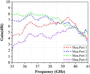
Fig.25(b) shows the setting positions of the X, Y, and Z axes of the MW6 millimeter-wave anechoic chamber and the way the antenna is placed. In Fig. 26, switching the feeds of the four ports can cause the antenna to switch the beam and observe the beam direction and peak gain results at 38 GHz. Figure 26 shows the simulated and measured radiation patterns after ports 1–4 are excited, respectively. Figure 27 is the frequency and gain curve of the proposed antenna. Table 2 shows that the measured and simulated beam angles of ports 1–4 are very close to the ideal ±15° and ±45° when operating at 38 GHz. The measurement results of port 1 and port 2 differ by 1°. In addition, the measured peak gains of ports 1–4 are 6.1, 7.3, 7.7, and 6.7 dBi, respectively. Although the measured peak gains of ports 1–4 are 1.4, 1.2, 0.9, and 0.8 dBi, respectively, lower than the simulation, the beam trends of the two are very close. At the same time, the error between the measured central beam angle and the calculated main beam angle is within about 1°, proving that this design can accurately provide the required radiation angle.
4 × 4 Butler-wide bandwidth patch antenna radiation pattern measurement environment. (a) Erection environment. (b) Antenna erection method.

Simulated and measured 2D radiation patterns of 4 × 4 Butler-wide bandwidth patch antenna.

Frequency and gain curve of the 4 × 4 Butler-wide bandwidth patch antenna.

Ports 1–4 main beam angle and peak gain

Figure 28 shows the normalized simulation and measurement results of the radiation direction when port 1 is switched to port 4. When the frequency is 38 GHz, the measured side lobe of port 1 is about −4.8 dBi, while the side lobe of port 4 is as low as −6 dBi. The lowest side lobes of port 2 and port 3 are −7 dBi and −9 dBi. Although the side lobes of port 1 are larger than those of other ports, the overall side lobes are very low and the direction of the main lobe is clear. This proves that the antenna has good transmission quality and radiation effect.
Normalized simulation and measurement results of radiation direction of 4 × 4 Butler-wide bandwidth patch antenna switching ports 1–4.

Literature discussion and comparison
Table 3 compares and analyzes the research on the Butler matrix in recent years with the proposed 4 × 4 Butler-wide bandwidth patch antenna. The table shows that the proposed antenna has a better bandwidth advantage than other studies. The antenna can cover the working frequency band of 33.8-43.1 and has a good bandwidth of 24.2%.The proposed antenna has a beam angle that is more accurate beam angle than [Reference Sun, Ban, Che and Nie10, Reference Chung, Lin and Yang36, Reference Shady and Kishk37, Reference Hussein, Rahim, Murad and Hanoosh43, Reference Sun, Ban, Li, Lian, Hu and Nie44] and only deviates from the ideal ±15° and ±45° by 1°. In the designs of refs [Reference Qin, Chen and Xiang1, Reference Zhu and Deng9, Reference Sun, Ban, Lian, Liu and Nie22, Reference Wu, Zhang, Zhou and Huang29], multi-layer boards or more complex design methods are used to achieve better bandwidth and gain. However, this article uses SIW technology to integrate components on a single-layer planar substrate to achieve good bandwidth and gain. At the same time, this production method also makes the overall cost lower and makes the antenna more practical. Although the slot antenna of [Reference Sun, Ban, Che and Nie10] is also integrated into a single-layer planar substrate and has a peak gain of 7.8–12.6 dBi, the antenna beam angle has an error of 3–5°. Therefore, the proposed antenna is very competitive with the performance of wide bandwidth, and low side lobes.
Comparison of Butler matrix antenna literature

*Ref = Reference, FBW = Fractional Bandwidth.
The impact of antenna on the human body
In the mm-Wave, when the wireless product transmit power exceeds 20 mW, Power Density (PD) will be evaluated for the 1 cm2 and 4 cm2 areas of the human body. The US Federal Communications Commission (FCC) specifies that the PD value cannot exceed 40 W/m2 and 10 W/m2 at 1 cm2 and 4 cm2, respectively. This criterion can be calculated from (11) [Reference Chung, Lin and Yang36]. Figure 29 shows the PD simulation results when the 4 × 4 Butler wide bandwidth patch antenna is placed on the human wrist. Table 4 shows the detailed values of the simulated PD. The simulation results show that the antenna is in the standard specification of PD, which confirms that the antenna has the characteristics to be used in wearable devices.
 \begin{equation}\begin{array}{*{20}{c}}
{{{\text{S}}_{{\text{inc}}}}\left( {A,\,d,\,{{\beta}_{\text{x}}}} \right) = \frac{1}{{\text{A}}} \smallint \limits_{\text{A}} Re[E(d,{{\beta}_{\text{x}}}) \times {{\text{H}}^{\text{*}}}\left( {d,\,{{\beta }_{\text{x}}}} \right)] \cdot {{\hat n}}ds}
\end{array}\end{equation}
PD simulation results of a 4 × 4 Butler-wide bandwidth patch antenna placed on the human wrist. (a) Schematic diagram of the antenna placed on the wrist. (b) 1 cm2. (c) 4 cm2.

PD simulation values of 4 × 4 Butler-wide bandwidth patch antenna when placed on a human wrist

Conclusion
This article proposes a 4 × 4 Butler wide bandwidth patch antenna, which can be applied to the 38 GHz mm-Wave. The antenna consists of a −90° hybrid coupler, a crossover, a −45° phase shifter, and a patch antenna. The antenna performs beam switching by exciting ports 1–4, and the generated beam angle can be accurately maintained at the ideal beam angle. The beam range is ±45° when port 1 and port 4 are excited, and the beam range is ±15° when port 2 and port 3 are excited. After switching four beams, the measured peak gain of the antenna can reach up to 8.5 dBi. Although the side lobes of port 2 and port 4 are higher than those of port 1 and port 4, the overall side lobe beams do not affect the main lobe beam, indicating that the matrix antenna has higher transmission quality. The measured results of this antenna can cover 33.8–43.1 GHz and have a wide bandwidth advantage of 24.2%. The above results confirm that the proposed 4 × 4 Butler-wide bandwidth patch antenna has better bandwidth advantages and good peak gain. Compared with the traditional Butler matrix structure, the Butler matrix in this article has a simpler structure and can maintain the beam angle range of ±45° and ±15° without using a 0° phase shifter. At the same time, the SIW structure is integrated and designed on a single-layer planar substrate, which is more cost-effective than multi-layer boards. The proposed antenna can also comply with PD standards when placed on the human body, which means that the antenna has characteristics that can be applied to portable devices. This antenna has a competitive advantage in future mm-Wave applications.
Acknowledgement
This work was supported by the National Science and Technology Council, Taiwan, R.O.C. under Grant NSTC 113-2221-E-027-068.
Funding statement
This research received no external funding.
Competing interests
The authors declare no conflict of interest.

MING-AN CHUNG received the B.Eng. and M.Eng. degrees in electronic engineering from the Chang Gung University, Taoyuan, Taiwan and the D.Eng. degree in electrical engineering from the National Taiwan University of Science and Technology (NTUST), Taipei, Taiwan, in 2003, 2005, and 2016, respectively. He is currently an Associate Professor with the Department of Electronic Engineering, National Taipei University of Technology (NTUT), where he also serves as the Leader of the Innovation Wireless Communication and Electromagnetic Applications Laboratory. His research interests include wireless communication propagation, intelligent robotics, self-driving vehicles, antenna design for various mobile and wireless communications, electromagnetic theory, and applications. He is also a Reviewer of many scientific journals, including the IEEE Transactions on Antennas and Propagation, IEEE Transactions on Industrial Informatics, Journal of Intelligent & Robotic Systems, IET Microwaves, Antennas and Propagation, IEEE Antennas and Wireless Propagation Letters, International Review of Electrical Engineering, International Journal on Communications Antenna and Propagation and AEÜ - International Journal of Electronics and Communications, and many international conferences, including ICRA, ICCE-TW, RFIT, ICBEB, EMCAR and SNSP.

CHIA-CHUN HSU received her M.S. degree in Electronic Engineering from the National Taipei University of Technology in 2024 and is currently pursuing a Ph.D. Her research interests include wireless communication propagation research, antenna design, AIOT, emotion recognition applications, and 3D printing technology applications.

CHIA-WEI LIN received his B.S. and M.S. degrees from Chung Yuan Christian University in 2007 and is currently pursuing a Ph.D. degree in Electrical Engineering at the National Taipei University of Technology. His research interests include wireless communication propagation research, antenna design, intelligent robotics research, and self-driving vehicle research, embedded systems, deep learning.