I. INTRODUCTION
The concept of impedance transforming coupled-line couplers has been first introduced in [Reference Cristal1], and followed in [Reference Ahn and Kim2–Reference Wincza, Gruszczynski and Kuta5]. It was shown that in such couplers, the obtainable impedance transformation ratio R is limited by inequality:
 $$R \le \displaystyle{1 \over {k_{cl}^2}}, $$
where k cl is coupling of the coupled-line section and in case of single-section coupled-line couplers equals the overall coupling k. The proposed in [Reference Wincza and Gruszczynski4, Reference Wincza, Gruszczynski and Kuta5] circuits are suitable for application in balanced circuits where directional couplers having equal terminating impedances at transmitted and coupled ports are needed, and equal power split (k = 0.707), between transmitted and coupled ports is required. Then pre-matching to transistors input/output low impedance can be realized simultaneously with power division to reduce the system complexity and occupied space. However, the maximum achievable impedance transformation ratio in such couplers equals R max = 2, which is insufficient for application in balanced amplifiers utilizing power transistors having typically very low-input impedance.
On the other hand, it has been recently shown in [Reference Sorocki, Staszek, Piekarz, Wincza and Gruszczynski6] that the utilization of left-handed (LH) transmission lines placed in between the coupled-line sections allows for decreasing the required coupling coefficient of the coupled-line sections, without affecting the coupling of the entire structure.
In this paper, we show that the limit (1) applies only to the utilized coupled-line sections and not to the nominal coupling of the designed directional coupler. Therefore, by lowering the coupling coefficient of coupled-line sections the transformation ratio R is increased, while the nominal coupling is ensured with the technique shown in [Reference Sorocki, Staszek, Piekarz, Wincza and Gruszczynski6]. The distinct differences between the proposed network and the one proposed in [Reference Sorocki, Staszek, Piekarz, Wincza and Gruszczynski6] are: (i) the characteristic impedances of the direct and the coupled lines are different and determined by the terminating impedances of respective ports; and (ii) the characteristic impedances of uncoupled LH transmission lines are also different and equal to the characteristic impedances of the direct and coupled lines, respectively. Therefore, the proposed couplers offer different properties and functionalities not reported until now. The presented approach has been theoretically investigated and validated by measurements of a 3 dB directional coupler having impedance transformation ratio equal R = 4.
II. THEORETICAL ANALYSIS
In [Reference Wincza, Gruszczynski and Kuta5] an approach to the design of impedance transforming directional couplers operating at the maximum achievable transformation ratio, i.e.:
 $${R_{max}} = \displaystyle{1 \over {k_{cl}^2}} $$
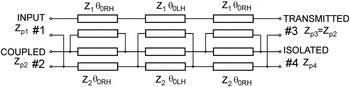
has been shown. In such a case, one coupled line is completely shielded by the second line allowing for the coupler to be modeled as an appropriate connection of two uncoupled transmission lines. Such an approach simplifies the analysis and is very convenient for the circuit design. On the other hand, lowering coupling coefficient of the coupled-line section below the nominal coupling of the designed directional coupler requires insertion of LH transmission-line sections having appropriate electrical length [Reference Sorocki, Staszek, Piekarz, Wincza and Gruszczynski6]. Taking this into account we have investigated the possibility of designing impedance transforming directional couplers in which the impedance transformation ratio is increased above the limit (2). The proposed circuit is shown schematically in Fig. 1.
Schematic diagram of the proposed impedance transforming directional couplers with enhanced transformation ratio realized as a connection of coupled-line sections (modeled as an appropriate connection of two uncoupled two-conductor transmission lines [Reference Wincza, Gruszczynski and Kuta5]) and ideal uncoupled LH transmission lines placed in between.

To investigate the properties of the proposed circuit, let us first consider the condition of impedance matching. Since both direct and coupled lines are transmission-line impedance transformers having the same transformation ratio R = Z p1/Z p3 = Z p2/Z p4, the conditions for ideal match can be derived from the properties of a lossless impedance transformer shown schematically in Fig. 2, and constituted of sections of right-handed (RH) and LH transmission lines. For the purpose of analysis, the LH transmission-line sections have been assumed ideal and modeled as shown in [Reference Sorocki, Piekarz, Wincza and Gruszczynski7].
Schematic diagram of an impedance transformer composed of sections of LH and RH two-conductor transmission lines.

The input impedance seen at port #1 can be calculated as:
 $${Z_{p1}} = {Z_1}\displaystyle{{{Z_{p2}} + j{Z_1}{\rm tan}(2{\theta _{0RH}} - \left \vert {{\theta _{0LH}}} \right \vert )} \over {{Z_1} + j{Z_{p2}}{\rm tan}(2{\theta _{0RH}} - \left \vert {{\theta _{0LH}}} \right \vert )}}.$$
In order to transform the impedance Z p1 into Z p2, two conditions must hold:
 $${Z_1} = \sqrt {{Z_{p1}}{Z_{p2}}},$$
 $$2{{\rm \theta} _{0RH}} - \left \vert {{{\rm \theta} _{0LH}}} \right \vert = 90^{\circ}.$$
Hence, the ideal match is obtained at the center frequency f 0 when the appropriate characteristic impedance Z 1 is chosen and the difference of electrical lengths equals quarter-wave.
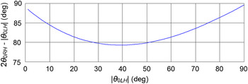
It was shown in [Reference Sorocki, Staszek, Piekarz, Wincza and Gruszczynski6] that the lowering of coupled-line coupling requirements of the directional coupler is only related to the electrical length of the coupled-line sections θ 0RH and uncoupled LH sections θ 0LH , while characteristic impedance can be arbitrarily chosen. Moreover, an approximate relation between θ 0RH and θ 0LH ensuring that the maximum of coupling function in such couplers is located at the center frequency has been given. Figure 3 presents the calculated value of diff = 2θ 0RH –|θ 0LH | versus the electrical length of the inserted LH transmission line, where electrical lengths are related as described in [Reference Sorocki, Staszek, Piekarz, Wincza and Gruszczynski6]. As it is seen the obtained results are in close agreement with the condition (4b), which confirms the possibility of applying the proposed method of lowering k cl in impedance transforming directional couplers. It is worth mentioning that the approximation given in [Reference Sorocki, Staszek, Piekarz, Wincza and Gruszczynski6] has been derived assuming weak coupling k ≈ 0, however the change of k in a wide range of values results in a small center frequency shift. For the considered coupler when coupling coefficient k is changing in the range of 0.1–0.5 the center frequency shifts lesser than 2.5%. The deviation of diff value from 90° results with frequency shift (from f 0) at which the impedance match has its minimum. To compensate that shift, the electrical lengths of all three subsections need to be scaled by the factor sf:
 $$sf \cong \displaystyle{{90^{\circ}} \over {2{\theta _{0RH}} - \left\vert {{\theta _{0LH}}} \right\vert}}. $$
The maximum of the coupling characteristic will be slightly shifted; however, the coupling bandwidth is much wider than the impedance match. Hence, it will not affect the circuit performance.
Electrical length of diff calculated assuming the relation between θ 0RH and θ 0LH from [Reference Sorocki, Staszek, Piekarz, Wincza and Gruszczynski6].

The above-presented analysis shows that impedance transformation and coupling can be realized independently. Note, that the chosen ratio R is still limited by the minimal required coupling of coupled-line sections needed for achieving the nominal coupling of the coupler. As an example, the minimum required coupling coefficient that allows for realization of 3-dB couplers according to [Reference Sorocki, Staszek, Piekarz, Wincza and Gruszczynski6] equals k cl ≈ 0.45; hence, the maximum achievable transformation ratio of the circuit proposed in Fig. 1 equals R ≈ 5 which is almost 2.5 times enhancement in comparison with condition (1).
The design of the proposed directional couplers having increased impedance transformation ratio can be summarized in the following steps:
-
• First, the desired impedance transformation ratio R and the overall coupling of the coupler k is chosen.
-
• Second, having chosen R, the coupling k cl of coupled-line sections is calculated from (2).
-
• Next, the characteristic impedances Z 1 and Z 2 of the transmission lines which model the coupled-line sections operating at the maximum impedance transformation ratio can be calculated as shown in [Reference Wincza, Gruszczynski and Kuta5].
-
• Finally, the electrical lengths of coupled-line sections θ 0RH and LH transmission lines θ 0LH are found based on [Reference Sorocki, Staszek, Piekarz, Wincza and Gruszczynski6] to achieve the nominal coupling of the coupler and subsequently scaled by factor (5) to maintain an ideal impedance match at the assumed center frequency.
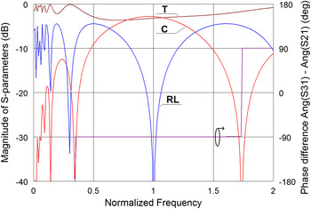
The proposed concept has been validated by ideal circuit simulations (see Fig. 4) of a 3-dB coupler composed of two 6-dB (k cl = 0.5) coupled-line sections and LH lines having electrical lengths equal θ 0RH = 66.9 and θ 0LH = 40°, respectively (C max = 2.8 dB at f = 0.96 and sf = 1.18). The utilization of the proposed technique allows one to realize a directional coupler having impedance transformation ratio R = 4, i.e. the termination impedances are equal: Z p1 = 50, Z p2 = Z p3 = 12.5, Z p4 = 3.125 Ω. The transmission line impedances are equal Z 1 = 21.65, Z 2 = 7.21 Ω (based on (18), (19) from [Reference Wincza, Gruszczynski and Kuta5]). As it is seen, the equal power split has been achieved as well as impedance transformation. The coupler features ideal isolation, and the bandwidth equal f u /f l = 1.24 assuming RL better than 15 dB.
Calculated S-parameters of a 3-dB impedance transforming directional coupler terminated with Z p1 = 50, Z p2 = Z p3 = 12.5, Z p4 = 3.125 Ω, initial θ 0LH = 33.9°, sf = 1.18: θ 0LH = 40°, θ 0RH = 66.9°, and C max = 2.8 dB.

III. EXPERIMENTAL RESULTS
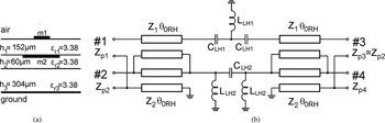
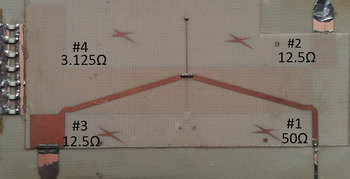
To experimentally verify the proposed concept, an exemplary coupler operating at the center frequency of f 0 = 1.2 GHz (parameters Z 1, Z 2, θ 0LH , and θ 0RH are assumed as in the previous section) has been designed, manufactured and measured. The circuit has been designed in a dielectric structure shown in Fig. 5(a) consisting of three dielectric layers where a middle layer h 2 is an adhesive layer to bond upper and lower laminates. Coupled-line sections have been realized as two (upper w 1 and lower w 2) strips having characteristic impedances Z 1 and Z 2, respectively. For the chosen dielectric structure the widths of the coupled-lines have been found: w 1 = 1.1, w 2 = 9.35 mm by numerical calculations using Linpar software [Reference Djordjevic, Bazdar, Sarkar and Harrington8] (metallization with zero thickness has been assumed). The physical length of the lower strip equals l 2 = 51.4 mm, whereas the upper strip's length equals l 1 = 53.6 mm and is slightly longer than the lower strip (see Fig. 6) to equalize the electrical lengths of both lines and to improve the overall couple's performance [Reference Wincza, Gruszczynski and Kuta5]. The LH transmission-line sections have been physically realized using their LC approximation. Based on [Reference Sorocki, Piekarz, Wincza and Gruszczynski7], for the required electrical length of θ 0LH , one subsection approximation is sufficient. The initial elements values of LH transmission line having the characteristic impedance Z 1 = 21.65 Ω has been realized in T-type topology and the LC elements’ values for such a network are equal L LH1 = 5.4 nH, C LH1 = 23.4 pF [Reference Sorocki, Piekarz, Wincza and Gruszczynski7]. For the second LH transmission-line having the characteristic impedance Z 2 = 7.21 Ω, π-type topology has been used and the elements’ values are: L LH2 = 3.66 nH, C LH2 = 14.9 pF. A schematic diagram of the circuit with physical realization of LH sections is shown in Fig. 5(b). In the designed exemplary coupler, series capacitances have been realized using SMD 0402 capacitors, whereas shunt inductors by using sections of high-impedance transmission-lines realizing appropriate reactance equal X L = Z L tan(θ 0L ) where the impedance Z L = 120 Ω has been chosen for practical realization. The coupler's performance is sensitive to the realization of transitions between appropriate parts of the circuit. Taking this into account, and since SMD components are available with quantifies values, final lumped elements values have been appropriately chosen.
Cross-sectional view of the utilized dielectric structure (a) and schematic diagram of the proposed circuit where LH transmission lines have been replaced by their LC approximations having n = 1 subsections (b).

A picture of the manufactured impedance transforming directional coupler having increased transformation ratio. The isolated port #4 has been directly terminated with SMD resistors.

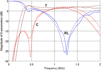
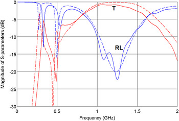
A picture of the manufactured impedance transforming directional coupler is presented in Fig. 6. Measured S-parameters with comparison to the theoretical ones are shown in Fig. 7, as it is seen a good agreement has been obtained. The measured characteristics are slightly shifted toward higher frequency, which is most likely caused by the significant influence of the parasitics related to connections between coupled and uncoupled lines. The obtained performance comparison of the proposed impedance transforming directional coupler with other works has been presented in Table 1. The distinct difference of the proposed coupler is its largest impedance transformation ratio R at the expense of bandwidth reduction, while the size, coupling imbalance and phase imbalance are comparable. In Fig. 8, the properties of the coupler have been verified in the balanced-circuit connection (back-to-back) which is its primary application as shown in [Reference Wincza and Gruszczynski4]. The achieved insertion losses equal 0.82 dB, which makes the circuit attractive in balanced networks.
S-parameters of the designed impedance transforming directional coupler. Solid lines represent the measurement results and dashed lines the calculated results of the ideal circuit shown in Fig. 5(b).

S-parameters of the balanced circuit obtained by a back-to-back connection of two impedance transforming directional couplers. Solid lines represent the measurement results and dashed lines the calculated results of the ideal circuit.

Performance comparison of the proposed circuit with other couplers presented in literature.

IV. CONCLUSION
A novel approach for the design of impedance transforming directional couplers has been proposed. It has been proved that the limit (1) applies only to the utilized coupled-line sections and not to the nominal coupling of the designed directional coupler, and therefore, it is possible to increase the coupler's impedance transformation ratio over the limit described in literature. Hence, the proposed solution is more suitable for application in balanced microwave power amplifier design, in which low-impedance transistors are utilized and allows for the design of e.g. 3-dB couplers having the impedance transformation ratio R > 2. The proposed technique has been verified by measurements of the manufactured 3-dB coupler having the transformation ratio R = 4, what is twice as high as for the known solutions. The obtained results prove the usability of the proposed approach.
ACKNOWLEDGMENTS
This work was supported in part by the National Science Centre, contract no. DEC-2011/01/D/ST7/00789 and in part by the Ministry of Science and Higher Education under contract no. 0510/IP2/2015/73.
 Jakub Sorocki received the M.Sc. degree in Electronics and Telecommunications from AGH University of Science and Technology (UST), Krakow, Poland in 2013 and currently working toward Ph.D. degree. Since 2011 he has been cooperating with Microwave Technology and High Frequency Electronics research group at the Department of Electronics, AGH UST. His scientific research interests focus on low-loss microwave circuits and left-handed metamaterials in microwave range. He has coauthored several journals and conference papers.
 Ilona Piekarz received the M.Sc. degree in Electronics and Telecommunications from AGH UST, Cracow, Poland in 2013 and currently working toward Ph.D. degree. Since 2011 she has been cooperating with Microwave Technology and High Frequency Electronics research group at the Department of Electronics, AGH UST. In 2013, she received “Diamond Grant” for outstanding students awarded by the Ministry of Science and Higher Education for her research on microwave biosensors. She has coauthored several journals and conference papers.
 Slawomir Gruszczynski received the M.Sc. degree and the Ph.D. degree in Electronics and Electrical Engineering from the Wroclaw University of Technology, Poland, in 2001 and 2006, respectively. Since 2001 to 2006 he has been with Telecommunications Research Institute, Wroclaw Division, From 2005 to 2009, he worked at the Institute of Telecommunications, Teleinformatics and Acoustics, Wroclaw University of Technology. In 2009, he joined the Faculty of Informatics, Electronics and Telecommunications at AGH University of Science and Technology where he became a Head of the Department of Electronics in 2012. He has coauthored more than 40 journal and 70 conference scientific papers. He is a member of the IEEE, and a member of Young Scientists’ Academy at Polish Academy of Sciences (PAN) and Committee of Electronics and Telecommunications at Polish Academy of Sciences (PAN).
 Krzysztof Wincza received the M.Sc. degree and the Ph.D. degree in Electronics and Electrical Engineering from the Wroclaw University of Technology, Poland, in 2003 and 2007, respectively. In 2007, he joined the Institute of Telecommunications, Teleinformatics and Acoustics, Wroclaw University of Technology. In 2009, he joined the Faculty of Electronics at AGH University of Science and Technology as an Assistant Professor. Dr. Wincza was the recipient of The Youth Award presented at the 10th National Symposium of Radio Sciences (URSI) and the Young Scientist Grant awarded by the Foundation for Polish Science in 2001 and 2008, respectively. He has coauthored more than 40 journal and 70 conference scientific papers.