Introduction
Millimeter-wave (mm-wave) technology has been proposed to be adopted for future fifth-generation (5G) communication systems due to its higher speed, wider bandwidth, higher capacity, and lower latency compared to the existing 4G/LTE technology. Consequently, different 5G new radio (5G NR) frequency bands have emerged in frequency range 2 (FR2) such as n257, n258, n260, and n261, with various band subsets assigned to different countries/regions. For instance, the mm-wave bands designated for the US include 24.25–24.45, 24.75–25.25, and 27.75–28.35 GHz, while for Canada, it is 26.5–27.5 and 27.5–28.35 GHz, and for India, it is 24.25–27.5 GHz. This presents an ongoing challenge to the antenna researchers to design a compact dual/multi-band antenna capable of handling dual/multiple beams with high port isolation for the future 5G NR systems operating at FR2. While the multiple bands can offer better spectrum utilization, the dual/multiple beams can improve spatial coverage and are also suitable for multiuser communication. This feature also supports different communication schemes such as spatial multiplexing and beamforming, which significantly improve signal quality, data rates, and mitigate interference [Reference Huang, Chen, Shiu, Wang and Chang1].
In recent years, few dual-beam antennas [Reference Liu, Shi-Shan, Wen and Fang2–Reference Jian-Feng, Chen, Duo-Long, Zhang and Yan-Jie12] are reported in the literature. The dual-band single-/dual-beam U-shaped slot antenna, presented in [Reference Liu, Shi-Shan, Wen and Fang2], utilizes  $\text{TM}_{10}$ mode in the lower band and
 $\text{TM}_{20}$ mode in the upper band. The main drawback of this antenna is that it provides single beam at the lower band. The dual-beam antennas, presented in [Reference Khidre, Lee, Elsherbeni and Yang3–Reference Chen, Guo and Wang5], use higher-order
 $\text{TM}_{02}$ mode for their operation. The drawback of antenna [Reference Khidre, Lee, Elsherbeni and Yang3] is its asymmetrical-beam pattern with 2 dB gain difference, whereas the literature [Reference Karmokar, Esselle and Bird4] suffers from its large size and frequency scanning behavior. The authors [Reference Chen, Guo and Wang5] achieve a symmetrical dual-beam pattern by virtue of its centrally located cross-shaped feeding probe, but it lacks compactness due to the large separation between ground plane and radiator. A dual-beam antenna, consisting of a quasi
 $\text{TM}_{02}$ mode patch at the top and SIW cavity at the bottom, separated by a substrate, is reported in [Reference Tan, Jiang, Gong, Cheng, Ren and Zhang6]. The issue with [Reference Tan, Jiang, Gong, Cheng, Ren and Zhang6] is its double-layer structure. Few dual-beam antennas also have been reported using metamaterial technology [Reference Jiang, Li-Ming, Weidong and Xin7–Reference Dadgarpour, Sorkherizi, Denidni and Kishk9]. The common drawback of these antennas is their bulky structure. The fractal dual-beam antenna, presented in [Reference Ullah and Tahir10], suffers from low gain. Two dual-beam filtering patch antennas, those operate using
 $\text{TM}_{02}$ mode, are presented in [Reference Jian-Feng, Mao, Duo-Long, Liang-Hua and Zhang11, Reference Jian-Feng, Chen, Duo-Long, Zhang and Yan-Jie12]. However, they are multi-layered structure and hence not compact. The circularly polarized dual-beam dual-mode antenna, presented in [Reference Tian, Tang, Guan, Wenchengzhang and Yiming13], use
 $\text{TM}_{220}$ mode for its operation. However, it suffers from low bandwidth. In [Reference Kumari and Das14], a dual-beam antenna element for sub-6 GHz 2-port multiple-input multiple-output (MIMO) applications. The dual-beam pattern is achieved by creating two weak field regions in an eighth-mode SIW. This MIMO antenna provides high port isolation but has a large size due to the use of separated radiators.
Recently, self-multiplexing antennas have gained increasing interest among the antenna designers as they can operate over multiple frequency bands without the need of any external frequency selective circuit, resulting in overall system compactness. In the study [Reference Khan and Mandal15], a self-diplexing antenna has been presented using  $\text{TE}_{210}$ and
 $\text{TE}_{120}$ resonant modes. Research [Reference Naseri, PourMohammadi, Melouki, Ahmed, Iqbal and Denidni16] present a Quarter-Mode SIW (QMSIW) self-diplexing antenna that uses two capacitive slots of different lengths to operate over two different bands. Another QMSIW-based self-diplexing antenna is presented in [Reference Pradhan, Subramanian, Barik and Cheng17]. Here, a Y-shaped slot is etched diagonally for enabling the antenna to operate over two frequency bands. The authors [Reference Kumar, Chaturvedi and Raghavan18] present two QMSIW cavities for radiation, split from an Half-Mode (HMSIW) by an open slot. The authors [Reference Nandi and Mohan19] present an SIW cavity-backed self-diplexing antenna that uses two transverse slots of different lengths to perturb two distinct resonant modes within the cavity, resulting two radiation bands. In Ref. [Reference Mukherjee and Biswas20], the authors use an offset bow-tie slot to excite two HMSIW cavity modes for dual-frequency radiation. In Ref. [Reference Syed, Almalki, Alzahrani and Alsalami21], isolator slot is placed on the cavity, splitting it into two unequal parts for dual-band radiation.
It may be noted that the antennas, reported in Refs [Reference Liu, Shi-Shan, Wen and Fang2–Reference Kumari and Das14], operate with a single port over single/multiple frequency bands, and hence they cannot be categorized as self-multiplexing antennas, whereas antennas presented in Refs [Reference Khan and Mandal15–Reference Mukherjee and Biswas20] act as self-diplexing antennas, but with a single beam at each port. Overall, the literature reveals that no multi-beam self-multiplexing antenna has been designed so far.
This paper presents, for the first time, a symmetrical dual-beam self-diplexing SIW antenna, having the following key features: (i) capability to support multi-user communication through dual-beam, (ii) independent frequency tuning capability that enhance design flexibility, (iii) enhanced port isolation, and (iv) optimized null depth. The geometry, operating principle, development stages, and parametric analysis of the antenna are presented in Section “Design of dual-beam self-diplexing slot antenna.” Section “Experimental validation” presents the simulated and measured results of the antenna, with the conclusion in Section “Conclusions.”
Design of dual-beam self-diplexing slot antenna
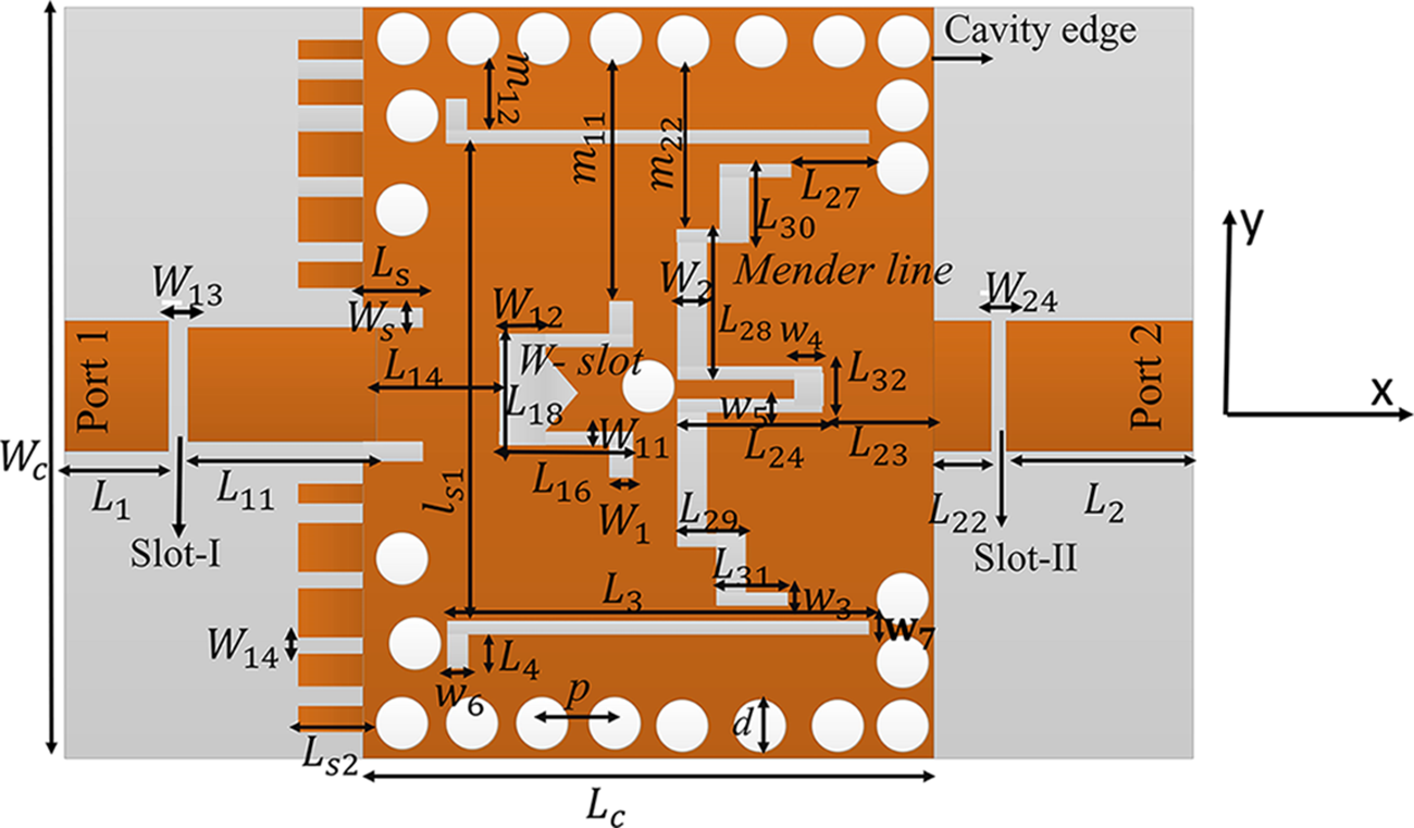
Figure 1 shows the proposed SIW cavity-backed symmetric dual-beam self-diplexing slot antenna. The antenna is designed using a 0.787 mm thick RT Duroid 5880 dielectric substrate of dielectric constant 2.2 and tan delta 0.0009 in the CST Microwave Studio full-wave simulator. The proposed antenna is designed using two steps: Step I and Step II. Step I includes the design of the self-multiplexing SIW cavity, whereas Step II includes the achievement of dual-beam antenna characteristics inside the self-multiplexing SIW cavity.
Schematic of the proposed SIW cavity-backed symmetric dual-beam self-diplexing slot antenna. The dimension of antenna are (Wc = 11.7, Lc = 10.31, L 1 = 2.08, L 11 = 3.55, L 2 = 3.6, L 22 = 0.89, Ls = 1.2, L 14 = 2.45, L 16 = 2.76, L 18 = 1.75,  $L_{s1}$ = 9.31,
 $L_{s2}$ = 0.88, L 23 = 2.32, L 27 = 2.76, L 24 = 2.1, L 28 = 2.75, L 29 = 1.16, L 30 = 1.03, L 31 = 1.05, L 32 = 0.63, m 12 = 0.912, m 11 = 3.61, m 22 = 2.03, L 3 = 8.26, L 4 = 0.62, d = 0.8, p = 1.3, Ws = 0.15, W 13 = W 14 = 0.3, W 12 = 1.5, W 11 = 0.15, W 1 = 0.39, W 24 = 0.2, w 3 = 0.15, w 4 = 0.34, w 5 = 0.19, W 2 = 0.55, w 7 = 0.13, w 6 = 0.4 (unit: mm)).

Step I (Design of the self-multiplexing SIW cavity)
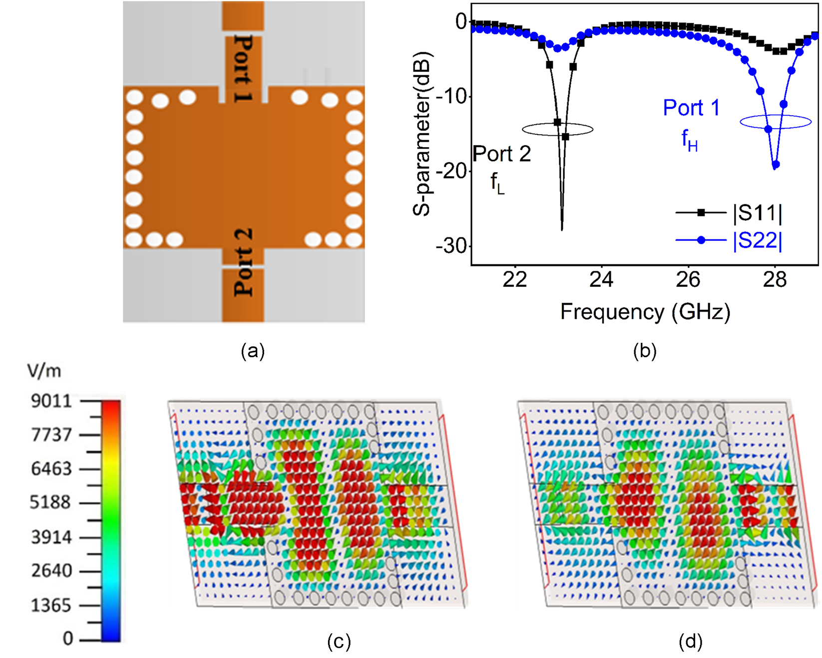
The schematic of the self-multiplexing SIW cavity is shown in Figure 2(a). The dimensions of the cavity are chosen to support the TE 20 mode. The SIW cavity is fed by two transverse slot-coupled microstrip feed lines, which act as Port 1 and Port 2 of the self-diplexing antenna. The transverse slots, referred to as Slot-I and Slot-II, are etched at different positions on their respective feed lines. These slots introduce capacitive loading to the cavity and can function as capacitive gap-coupled resonator bandpass filter (CGCR BPF). By varying the slot position, the resultant capacitive loading to the cavity can be varied, which helps to tune the resonant frequency of the cavity. The frequency responses of the structure are shown in Figure 2(b). It reveals that for Port 1 excitation the cavity resonates at 27.9 GHz (Figure 2(b), black curve), whereas for Port 2 excitation, it resonates at 23.1 GHz (Figure 2(b), blue curve). The vector E-field distributions inside the cavity for Port 1 and Port 2 excitations are shown in Figure 2(c) and (d), respectively. It reveals that the cavity operates with the TE 20 mode for both Port 1 and Port 2 excitations.
(a) Schematic of the self-diplexing SIW cavity, (b) frequency responses of cavity; Vector E-field distribution inside the cavity for (c) Port 1 excitation at 27.2 GHz, and (d) Port 2 excitation at 23.1 GHz.

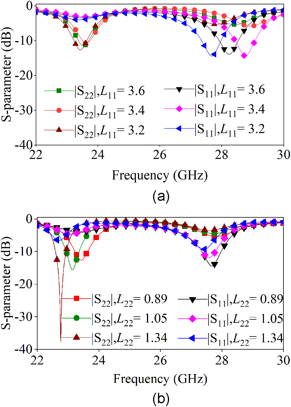
In order to study the effects of the positions of the CGCR BPFs on the frequency responses of the cavity, parametric analysis of the structure Figure 2(a) has been carried out with respect to the parameters L 11 and L 22. The results are shown in Figure 3. It reveals that when L 11 is varied from 3.2 to 3.6 mm, the Port 1 resonance frequency varies from 28.75 to 27.6 GHz, with slight variation of the Port 2 resonance frequency Figure 3(a). Similarly, when L 22 is varied from 0.89 to 1.34 mm, the Port 2 resonance frequency varies from 23.45 to 22.79 GHz, with slight variation of Port 1 resonance frequency Figure 3(b). The variation of the excited port resonance frequencies is due to the variation of the capacitive loading due to the changes in capacitive gap positions. The slight variation in coupled port resonance frequency is due to the finite coupling between the ports, which can be removed if the ports can be decoupled, as will be evident later.
Effect of (a) L 11 and (b) L 22 on frequency responses of the cavity Figure 2(a).

Step II (Achievement of dual-beam antenna characteristic)
Operating principle of dual beam antenna
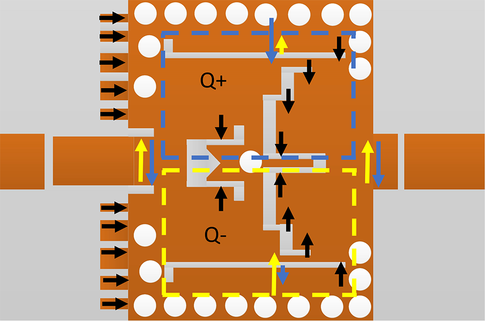
The dual-beam antenna features inside the designed self-multiplexing SIW Cavity in Step I is achieved following operating principle of field destruction method as depicted in Figure 4. The E-fields radiated by the individual horizontal slots of lengths L 3, L 16, L 24, L 29, and L 31 are shown by the black arrows, whereas the net E-fields radiated by the slots located on +y (Q+, shown by dotted blue rectangle) and −y (Q−, shown by dotted yellow rectangle) quadrants are represented by the blue and yellow arrows, respectively. By placing the slots symmetrically with respect to the y = 0 axis and exciting the cavity with the TE 20 mode the magnitude and direction of these net E-fields can be made equal and opposite along the y = 0 axis, resulting in a null along the broadside direction. However, due to different distances of the Q+ and Q− quadrant slots from the lower (y = − Wc/2) and upper (y = + Wc/2) edges of cavity, respectively, the −y and +y directed E-fields from the Q+ and Q− quadrant slots will not be able to completely cancel each other along the cavity edges. Therefore, a net E-field will exist along the lower and upper edges of cavity, and a split dual-beam pattern with a broad-side null is obtained.
Operating principle of self-diplexing dual-beam antenna.

Development stage of dual-beam antenna
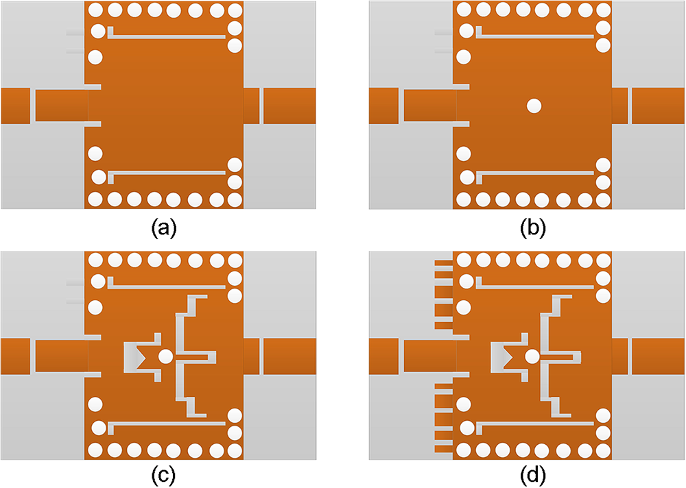
The development stages of the dual-beam antenna are shown in Figure 5.
Development stage of the antenna. (a) Stage I, (b) Stage II, (c) Stage III, and (d) Stage IV.

Stage I: In Stage I, two offset half-wavelength radiating L-slots (slot offsets y =  $l_{s1}$/2 and optimized slot length (L 3 + L 4) = 0.52
 $\lambda_{g,m}$, where
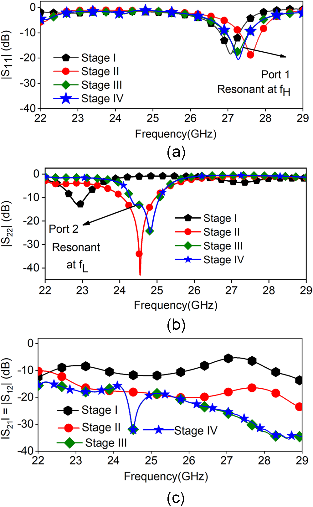
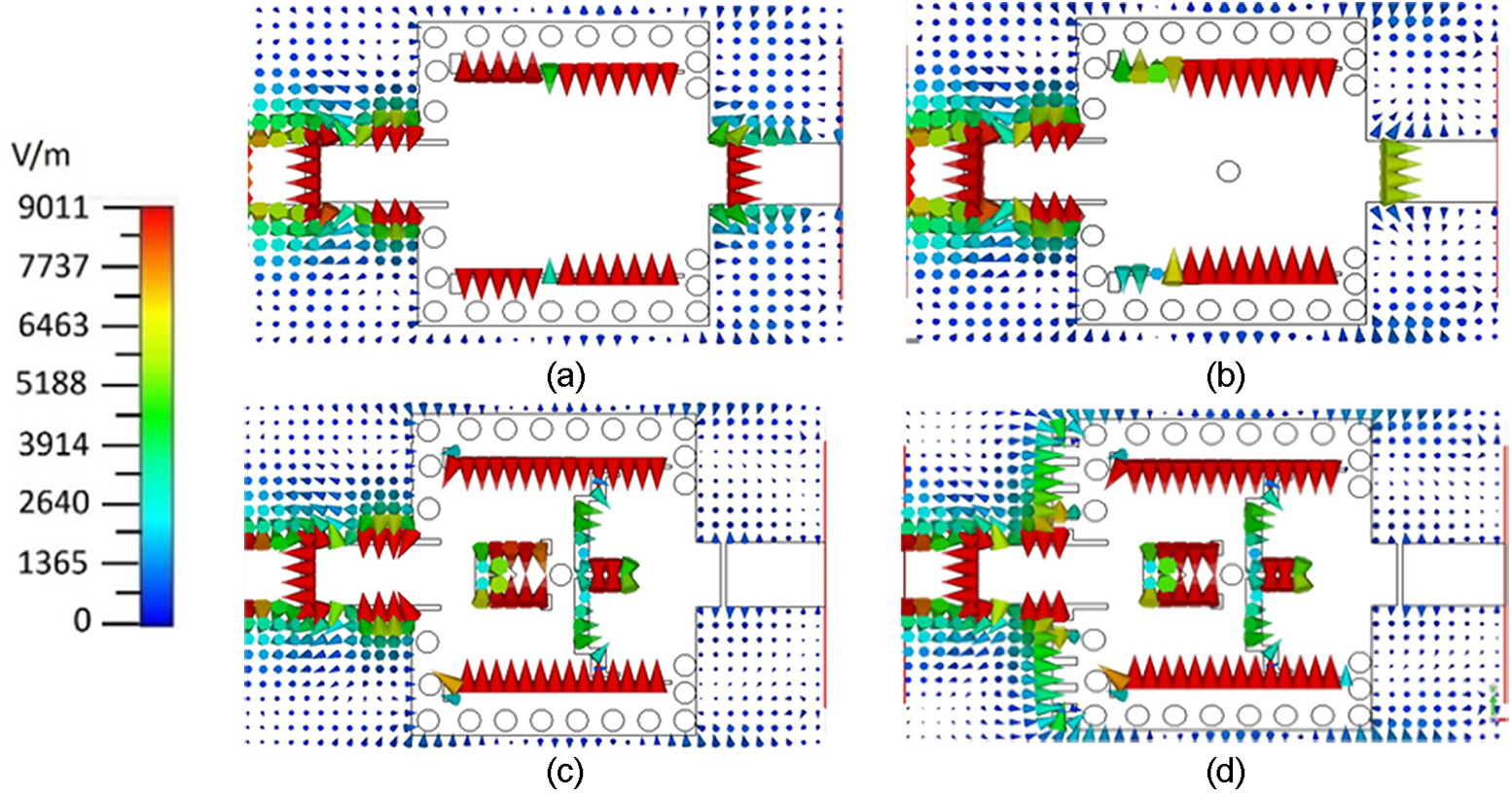
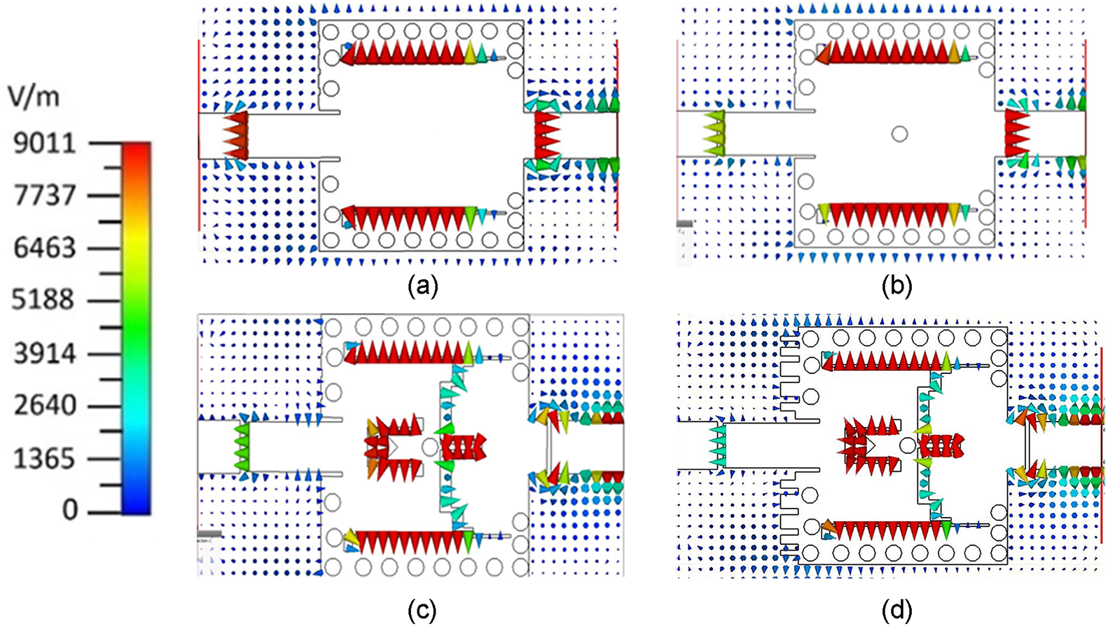
 $\lambda_{g,m}$ is guided wavelength at the mean frequency, fm = (fL + fH)/2) are etched on the cavity, as shown in Figure 5(a). The frequency responses of the antenna are shown in Figure 6 (black curve). It reveals that for Port 1 excitation the antenna radiates at 27.06 GHz (Figure 6(a), black curve), whereas for Port 2 excitation it radiates at 22.87 GHz (Figure 6(b), black curve). It further reveals that port isolations are very poor, around 10 dB (Figure 6(c), black curve). In order to illustrate the high port coupling, the vector E-field distributions on the Stage I antenna are shown in Figure 7(a) for Port 1 excitation and in Figure 8(a) for Port 2 excitation. They reveal the presence of significant E-field at Port 2 and Port 1 capacitive gaps for Port 1 and Port 2 excitation, respectively, which results in poor port isolation. In Figure 7(a), the opposite-phase polarity of the cavity mode (TE 20) couples with the L-shaped slots, resulting in destructive interference and weak radiation.
Frequency responses of the dual-beam antenna at each development stage. (a)  $|S_{11}|$, (b)
 $|S_{22}|$, and (c)
 $|S_{21}|$.

Vector E-Field distribution on the antenna for Port 1 excitation. (a) Stage I at 27 GHz, (b) Stage II at 27.6 GHz, (c) Stage III at 27.2 GHz, and (d) Stage IV at 27.3 GHz.

Vector E-Field distribution on the antenna for Port 2 excitation. (a) 22.8 GHz (Stage I), (b) 24.52 GHz (Stage II), (c) 24.82 GHz (Stage III), (d) 24.95 GHz (Stage IV).

Stage II: To reduce the high port coupling of Stage I antenna, a shorting via has been introduced at the center of the cavity in development Stage II Figure 5(b). The frequency responses of the Stage II antenna are shown in Figure 6 by the red curves. It reveals that for Port 1 excitation the antenna radiates at 27.60 GHz (Figure 6(a), red curve), whereas for Port 2 excitation the antenna radiates at 24.54 GHz (Figure 6(b), red curve). The upshift of the Stage II antenna operating frequencies is attributed to the shorting via, which provides an additional shunt inductance in the cavity. This shunt inductance appears in parallel with the shunt inductances of the SIW vias and thus decreases the overall inductance in the system, resulting in an upshift of the operating frequencies. The shorting via also acts as a decoupling network between Port 1 and Port 2, thus improves port isolation. The plot of  $|S_{12}|$ (or
 $|S_{21}|$) data in Figure 6(c) (in red curves) shows that the port isolation has been improved significantly and is <16 dB within the 10 dB return loss bandwidths. The improvement in port isolation can be illustrated by studying the vector E-field distributions on the Stage II antenna (Figures 7(b) and 8(b) for Port 1 and Port 2 excitations, respectively), which show that the E-field at the capacitive gap of the coupled port has been reduced significantly. As Figure 7(b) shows, introduction of a shorting via splits the cavity into two half-cavity. This prevants destructive interference by allowing the L-shaped slots to couple with one half-cavity section while the via blocks signal propagaion to other section. As a result, oppositely directed vectored E-field appears in the two L-slots, leading to a dual-beam radiation.
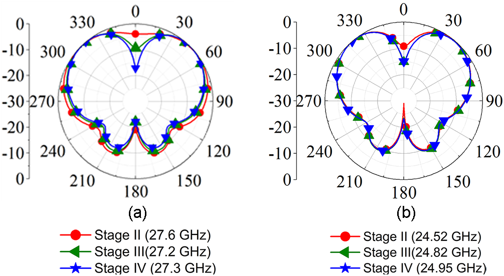
Stage III: The yz-plane ( $\phi=90^\circ$) radiation patterns of the Stage II antenna for Port 1 and Port 2 excitations are shown in Figure 9 by the red curves. They reveal that the Stage II antenna has a dual-beam pattern but with a very poor broadside null depth (approximately, −3.9 dB for Port 1 and −9.5 dB for Port 2 excitation). In order to solve this issue, a W-shaped slot and a mender line slot have been etched on the Port 1 and Port 2 sides of the shorting stub, respectively (Figure 5(c), Stage III). The lengths of the W-slot and mender line-slot were initially taken as 0.5
 $\lambda_{g,m}$ and
 $\lambda_{g,m}$, respectively, and later were optimized for an acceptable response. The optimized lengths are 0.43
 $\lambda_{g,m}$ and 0.86
 $\lambda_{g,m}$, respectively. The slots are etched symmetrically along the y = 0 axis of the cavity. The frequency responses of the Stage III antenna are shown in Figure 6 by green curves. It reveals that the antenna radiates at 27.27 GHz for Port 1 excitation (Figure 6(a), green curve) and at 24.82 GHz (Figure 6(b), green curve) for Port 2 excitation. The isolation plot of the Stage III antenna, shown in Figure 6(c) by the green curve, reveals that the port isolation has been improved. This is due to the additional series capacitances in the cavity due to the W- and mender line slots. The vector E-field distributions on the Stage III antenna for Port 1 and Port 2 excitations are shown in Figures 7(c) and 8(c), respectively, which reveal that the E-fields on the horizontal slots L 16, L 24, and L 3 are of equal magnitude and oppositely directed (±y-directed) facilitate the complete field cancellation in the null direction of cavity. This results in a dual-beam radiation pattern with a broadside null. In order to verify this, the radiation patterns of the Stage III antenna are plotted in Figure 9 (green curves) for Port 1 and Port 2 excitations. They reveal a dual-beam pattern for both port excitations. However, it is also observed that for Port 1 excitation, the null depth is still poor, i.e. −5.1 dB while for Port 2 it is significantly improved to −16.39 dB.
Polar radiation pattern for each development stage of dual-beam antenna. (a) Port 1 excitation and (b) Port 2 excitation on yz plane ( $\phi = 90^\circ$).

Stage IV: In order to improve the broadside null depth of the Port 1 radiation pattern, a corrugated microstrip structure has been incorporated at the Port 1 side of the cavity, as shown in Figure 5(d), resulting in the Stage IV or final antenna. The frequency responses of the Stage IV antenna are shown in Figure 6 in blue colors, which reveal that they are almost the same as those of the Stage III antenna. This is due to the fact that the corrugations are made outside the cavity (separated by electric via walls) and hence do not significantly affect the cavity input impedance. The vector E-field distribution on the Stage IV antenna for Port 1 excitation, shown in Figure 7(d), reveals that the corrugation introduces additional E-fields surrounding it, which destructively interfere with the finite broadside radiation of the Stage III antenna and enhance the null depth along it. The radiation patterns of the Stage IV antenna are shown in Figure 9 in blue curves, which reveal that the broadside null depth for Port 1 excitation has been improved to −17.8 dB. Since Port 2 is already decoupled, such modification does not affect the Port 2 radiation pattern.
Parametric study of dual-beam antenna
Parametric analysis of the antenna with respect to few of its important geometrical parameters are presented below.
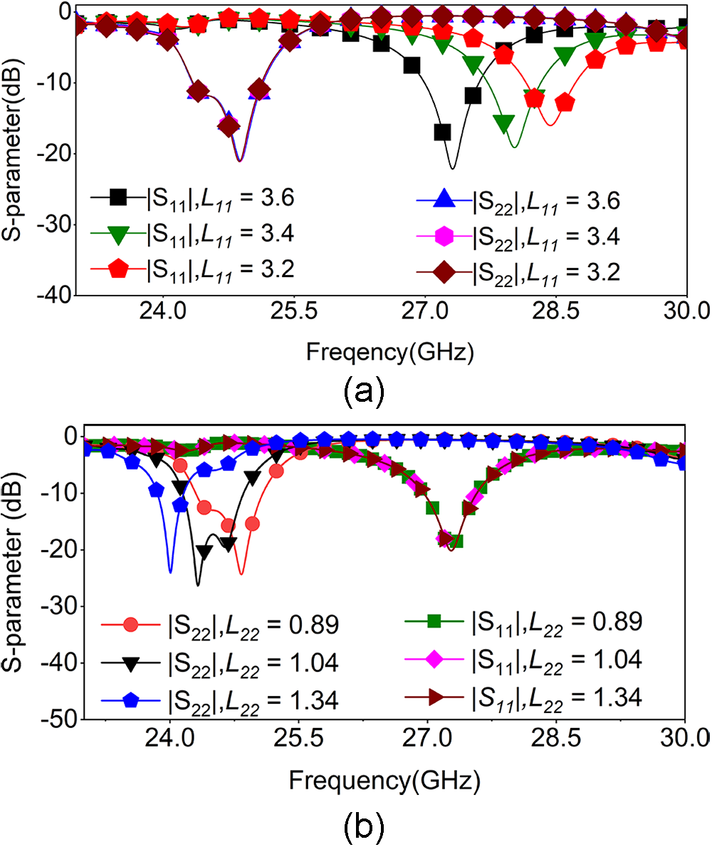
Independent frequency tunability: The effect of the positions of the capacitive coupling gaps (L 11 and L 22) on the frequency responses of the antenna is shown in Figure 10. It reveals that when L 11 is increased from 3.2 to 3.6 mm, the Port 1 band moves toward the lower frequency, whereas the Port 2 band remains unaffected Figure 10(a). Similarly, Figure 10(b) reveals that when L 22 is increased from 0.89 to 1.34 mm, the Port 2 band moves toward the lower frequency, whereas the Port 1 band remains unaffected. It can be shown that L 11 and L 22 have no major effect on the port isolation. This is due to the fact that the variation of the gap position changes the net input impedance of the antenna at the ports. However, since the ports are decoupled, they do not affect the other port characteristics. Thus, L 11 and L 22 can be optimized to independently position the respective band without affecting the isolation characteristics. It may be noted that fL and fH are not limited to the original bandwidth for the TE 20 mode of the cavity.
Effect of (a) L 11 and (b) L 22 on the  $|S_{11}|$ and
 $|S_{22}|$ frequency responses of the dual-beam antenna.

During the design of the antenna the electrical length of L 11 was initially set to 0.5 $\lambda_{g,fH}$ and later optimized to 0.48
 $\lambda_{g,fH}$, where
 $\lambda_{g,fH}$ is guided wavelength upper operating frequency fH. Similarly, electrical length of L 22 was initially 0.125
 $\lambda_{g,fL}$ and later optimized to 0.108
 $\lambda_{g,fL}$, where
 $\lambda_{g,fH}$ is the guided wavelength at the lower operating frequency fL. Different electrical lengths for L 11 and L 22 were chosen to achieve the diplexing property in the cavity, as stated earlier.
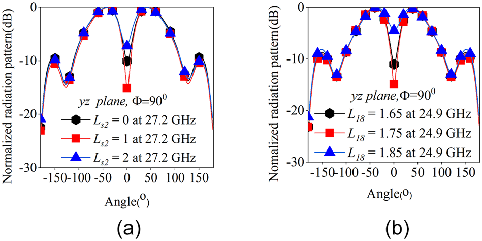
Independent control of broadside null depths: The effect of the corrugation width  $L_{s2}$ on the Port 1 yz-plane, (
 $\phi = 90^\circ$) radiation pattern of the antenna is shown in Figure 11(a). It reveals that
 $L_{s2}$ can be varied to control the broadside null depth of the Port 1 radiation pattern. In order to control the broadside null depth of the Port 2 yz-plane, (
 $\phi = 90^\circ$) radiation pattern, the W-slot base width L 18 can be varied, as evident in Figure 11(b). It can be shown that Port 2 and Port 1 radiation patterns remain unaffected with the variation of
 $L_{s2}$ and L 18, respectively. Therefore,
 $L_{s2}$ and L 18 can be used to independently control the broadside null depths of the Port 1 and Port 2 radiation patterns, respectively. The lengths of the
 $L_{s2}$ and L 18 were initially taken as 0.125
 $\lambda_{g,fH}$ and 0.125
 $\lambda_{g,m}$ respectively, and later were optimized for an acceptable response. The optimized electrical length are 0.118
 $\lambda_{g,fH}$ and 0.103
 $\lambda_{g,m}$, respectively.
Effect of (a)  $L_{s2}$ on the Port 1 and (b) L 18 on the Port 2 radiation patterns on yz plane (
 $\phi = 90^\circ$).

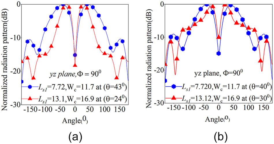
Optimizing beam direction control: Figure 12 demonstrates that by adjusting the cavity width Wc and separation between the L-slots  $L_{s1}$, the beam directions can be controlled. It may be noted here that this control of the beam directions by varying the Wc and
 $L_{s1}$ is not independent because any variation in these parameters also results in the change of the operating frequencies and null depths. Therefore, in order to control the beam directions by maintaining the operating frequencies and null depths, the following steps are used. In Step 1, the Wc and
 $L_{s1}$ should be optimized first to place the beams in suitable directions. In Step 2, the L 11, L 22,
 $L_{s2}$, and L 18 parameters should be optimized to locate the bands in the proper position and achieve the required broadside null depths.
Effect of  $L_{s1}$, Wc on the beam directions of (a) Port 1 at 27.1 GHz and (b) Port 2 radiation patterns 25 GHz on yz plane (
 $\phi = 90^\circ$).

Experimental validation
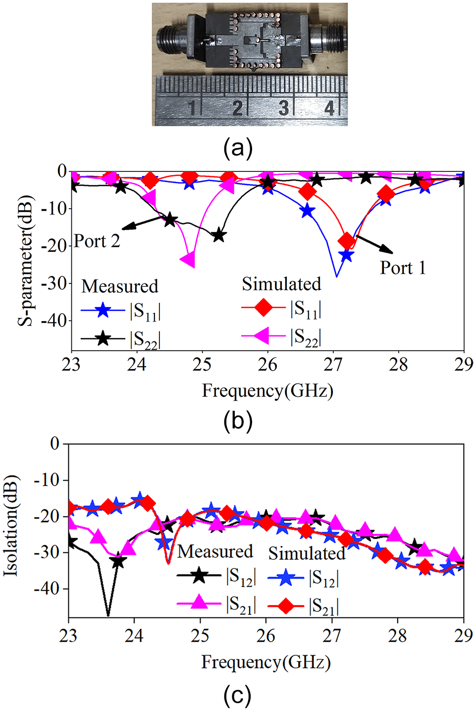
The frequency responses of the fabricated proposed antenna, shown in Figure 13(a), have been measured using a Rhode and Schwartz ZVA 50 vector network analyzer, and the measured frequency responses have been compared with the simulated frequency responses in Figure 13(b) and Figure 13(c). The results are summarized in Table 1. The plots reveal that the measured responses are in close agreement with the simulated responses. The slight discrepancies may be due to the parasitic effects of solder joints of the vias and SMA connectors.
(a) Fabricated antenna, (b) simulated and measured  $|S_{11}|$ and
 $|S_{22}|$ frequency responses, and (c) simulated and measured
 $|S_{12}|$ and
 $|S_{21}|$ frequency responses.

Comparison of simulation and measured result of proposed antenna

Note: IBW = impedance bandwidth.
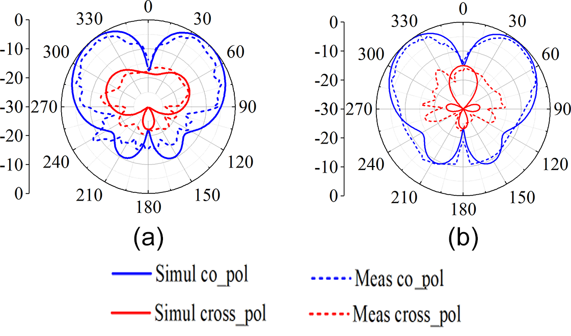
The simulated and measured normalized co-polarization and cross-polarization Port 1 and Port 2 radiation patterns of the antenna on the yz-plane are plotted in Figure 14(a) and (b), respectively. Since there is a null on the xz plane, normalized co-polarization and cross-polarization Port 1 and Port 2 radiation patterns of the antenna on the xz plane are not plotted. Figure 14(a) demonstrates that the simulated and measured cross-polarization levels are below −15 and −15.96 dB, respectively, for Port 1 excitation. Similarly, Figure 14(b) demonstrates that the simulated and measured cross-polarization levels are below −26.9 and −18 dB, respectively, for Port 2 excitation. For both Port 1 and Port 2 excitation, the simulated and measured beam directions are along  $\theta = \pm 43^\circ$ and
 $\theta = \pm 39^\circ$ (
 $\Phi = 90^\circ$), respectively. The half-power beam width of each beam is 56∘, determined with respect to the maximum radiated power of each beam.
Normalized 2D co-polarization and cross-polarization polar patterns for (a) Port 1 excitation at 27.25, and (b) Port 2 excitation at 24.85 GHz on yz plane ( $\phi = 90^\circ$).

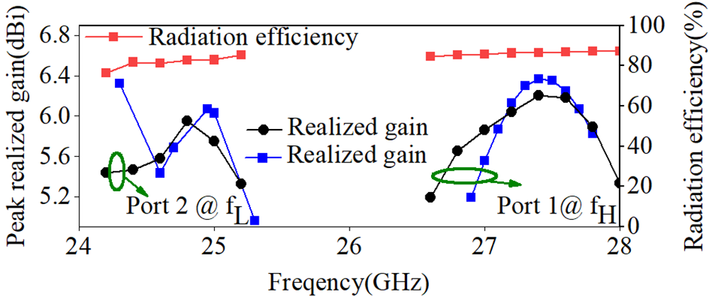
The simulated and measured peak realized gains and simulated radiation efficiency of the antenna are plotted in Figure 15. It reveals that the measured peak realized gain of the antenna at 27.4 GHz for Port 1 excitation is 6.21 dBi, whereas the measured peak realized gain of the antenna at 24.8 GHz for Port 2 excitation is 5.95 dBi. It also shows that the radiation efficiency varies from 83% to 86% for Port 1 excitation and 76% to 84% for Port 2 excitation.
Realized gain and radiation efficiency of the antenna.

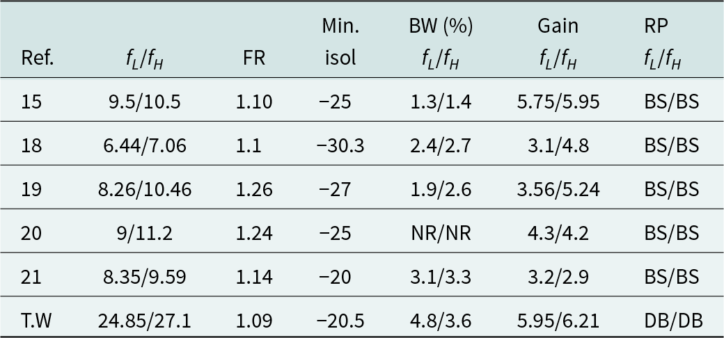
Table 2 presents a comparison of the characteristics of the proposed dual-beam self-diplex antenna with several other reported self-diplexing antennas. It demonstrates that the proposed antenna offers higher gain, higher percentage bandwidth, and a lower frequency ratio compared to others. Additionally, it provides symmetric dual-beam, whereas the other antennas provide a single broadside beam.
Comparison of proposed antenna with other reported self-diplexing antennas

Note: fL and fH are lower band and upper band center frequency. FR = frequency ratio; Min. isol = minimum isolation in (dB); BW % = fractional bandwidth; T.W = this work, gain in dBi; RP = radiation pattern; BS = broad-side; DB = dual-beam.
Conclusions
This paper presents a novel SIW cavity-backed symmetrical dual-beam self-diplexing slot antenna for short-distance multiuser point-to-point communications in the mm-wave frequency band. It also can be used in multi-patient monitoring in biomedical sensing and multi-object tracking in automotive radar. The antenna operated from 24.29 to 25.10 GHz in the lower band, whereas 26.95–27.57 GHz in the higher band. Further, by varying the position of the capacitive gap, the individual bands can be repositioned independently without affecting the port isolation. Therefore, it is a suitable candidate for Canadian 26.5–27.5 GHz, Indian 24.25–27.5 GHz, and United States 24.25–24.45 and 24.75–25.25 GHz bands. It also offers desirable radiation characteristics such as better than 5.95 dBi peak-realized gain and better than −15 dB cross-polarization level. By operating at two independent frequencies and utilizing spatial beam separation (±43∘), it can mitigate signal interference and phase collision.
Acknowledgements
The work is partially supported by DST–FIST project and authors acknowledge its support in carrying out the work.
Competing interests
The author declares that there is no conflict of interest.

Prativa Swain received the M.Tech. degree Microwave engineering from VSSUT, Burla, India, in 2017. Since 2018 she has been with the IIT, Dhanbad, India, pursuing her Ph.D. degree Microwave engineering. Her current research interest includes design and development mm-wave antenna.

Sushrut Das obtained B.Sc. degree (with Physics Hons.), in 1999, M.Sc. degree in Physics with specialization in Electronics in 2001, M.Tech. degree in Microwave Engineering in 2003, and Ph.D. degree in Engineering in 2007. His area of specialization is RF networks and antennas. He has published 61 journal and 63 conference papers. He received URSI Young Scientist Award in Istanbul, Turkey on 2011.