Introduction
The discovery of graphene and the subsequent work have inspired the investigation of two-dimensional compounds made from elements other than carbon. In particular, silicene, a monolayer of silicon atoms arranged in a honeycomb lattice, has gathered considerable excitement because of silicon’s central role in the semiconductor industry [Reference Restrepo, Mishra, Goldberger and Wind1, Reference Kara, Enriquez, Seitsonen, Voon, Vizzini, Aufray and Oughaddou2]. Like graphene, it is also a zero–band gap semiconductor, with charge carriers as massless Dirac fermions, which leads to a very high carrier mobility. Both theoretical and experimental studies show that silicene possesses longer bond lengths and a slight buckled structure which is different from the planar structure of graphene [Reference Cahangirov, Topsakal, Akturk, Sahin and Ciraci3]. Although C and Si belong to the same group of the periodic table, Si has a larger ionic radius which promotes sp 3 hybridization. Quasi one-dimensional nanostructured materials derived from silicene, called silicene nanoribbons (SiNRs), have received an increasing amount of interest because of their electronic, magnetic, and thermal properties.
One advantage of silicene over graphene is that it is expected to be compatible with existing silicon-based electronics [Reference Pei, Zhang, Sha and Shenoy4]. Although significant research in the field of graphene nanoribbons is growing rapidly, its integration into current Si-based technologies faces a challenge [Reference Shuai and Wang5]. If silicene nanoribbons could be grown, their integration into Si-based nanoelectronics would be favored over graphene which will offer potential advantages of performance enhancement in high-speed miniaturized electronic devices [Reference De Padova, Perfetti, Olivieri, Quaresima, Ottaviani and Le Lay6]. The existence of silicene nanoribbons has been demonstrated recently in experiments. They have been synthesized on gold(110) [Reference Tchalal, Enriquez, Mayne, Kara, Roth, Silly, Bendounan, Sirotti, Greber, Aufray, Dujardin, Ali and Oughaddou7], silver(111) [Reference Tchalala, Enriquez, Mayne, Kara, Dujardin, Ali and Oughaddou8], iridium(111) [Reference Meng, Wang, Zhang, Du, Wu, Li, Zhang, Li, Zhou, Hofer and Gao9], and zirconium diboride(0001) [Reference Fleurence, Friedlein, Ozaki, Kawai, Wang and Takamura10] substrates as per the literature.
In the last few years, extensive research on heat transport has been demonstrated and efforts are made to modify the phonon thermal conductivity via defects, vacancies, impurities, tailored geometric shapes, strain etc. Among these methods, applied strain could be one of the most worthwhile candidates which can be used to tune the properties to pursue at the nanoscale [Reference Hu, Zhang and Poulikakos11]. The effects of strain on the thermal conductivity and thermoelectric properties of planar graphene have been studied extensively. However, little is known about its influence on silicene. The intrinsic physical properties of silicene, such as lattice thermal conductivity, have been an active area of research. Several numerical simulations have predicted the thermal conductivity of silicene nanoribbons. Compared with the extensive research on their structural, electronic, and thermal properties, the thermoelectric properties remain largely unexplored. The effect of strain on the thermoelectric properties of planar graphene nanoribbons has been extensively investigated recently. However, very little is known about how strain affects the thermoelectric properties of silicene nanoribbons.
In real devices, pores on one hand are not avoidable, but on the other hand, they can be used to improve the device performance. Kaur et al. suggested an enhancement in ZT with the increase in the pore size for armchair graphene nanoribbons (AGNRs) [Reference Kaur, Narang and Randhawa12]. In addition, mechanical deformation especially strain is almost inevitable during the fabrication process of nanostructures. Strain engineering has become an interesting area of research for continuously tuning the electronic and phononic properties and, hence, the thermoelectric properties of the nanostructures. Thermal properties of AGNRs under tensile and compressive strain have been extensively conducted [Reference Yeo, Loh and Gan13, Reference Wei, Xu, Wang and Zheng14, Reference Yeo, Sullivan, Loh and Gan15, Reference Zhai and Jin16]. Kaur et al. established relations between the pore size and the nature of strain for enhanced thermoelectric performance in AGNRs. Irrespective of the pore size, the performance improves at a compressive strain of 10%, although for tensile nature, the minimum cut-off strain required for improved ZT shows an inverse relation with the pore size [Reference Kaur, Narang and Randhawa17]. Owing to the fact that porous nanostructures offer a better environment for thermoelectric performance, there is a need to study the combined effects of these factors in armchair silicene nanoribbons (ASiNRs) as well. Although, present research studies analyze the effects of tensile strain on SiNRs [Reference Pei, Zhang, Sha and Shenoy4, Reference Hu, Zhang and Poulikakos11], but to the best of our knowledge, their thermoelectric properties under compressive strain are less known so far. Thus, there is a need for the detailed investigation of thermoelectric performance of strain-engineered porous ASiNRs as a function of pore morphology and applied temperature.
Restrepo et al. predicted the change in the nature of the band gap and mobility on the application of strain to silicane [Reference Restrepo, Mishra, Goldberger and Wind1]. Pei et al. studied the effects of tensile strain and isotopic doping on the thermal conductivity of silicene and found that the thermal conductivity increases at small tensile strains of up to 4% but decreases at larger strains [Reference Pei, Zhang, Sha and Shenoy4]. Armchair silicene nanoribbons have been analyzed for their structural and electronic properties to study the variation in the band gap under external transverse electronic fields. Hu et al. studied the thermal conductivity behavior of silicene and silicene nanoribbons and found that their thermal conductivity initially increases dramatically with applied tensile strain and thereafter fluctuates at an elevated plateau [Reference Hu, Zhang and Poulikakos11]. An et al. investigated the thermoelectric properties of zigzag silicene nanoribbons with the introduction of linear vacancies and found a strong spin Seebeck effect at room temperature [Reference An, Wang, Vasilopoulos, Liu, Chen, Dong and Zhai19].
In this study, using the semiempirical approach, we focus on the thermoelectric properties of porous ASiNRs under the influence of tensile and compressive strain with varying magnitudes so as to establish relations between the pore size and the nature and magnitude of strain for enhanced thermoelectric performance. The results obtained from this study discuss the possibility of using strain to tailor the functionality of silicon-based nanodevices.
Results and discussions
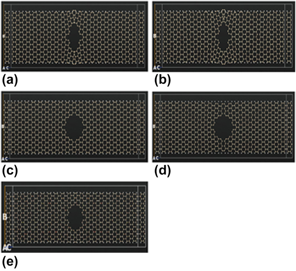
Here, the variation of thermoelectric performance of porous silicene nanoribbons with pore diameters of 1.55, 1.94, and 2.32 nm under a tensile and compressive strain of 5 and 8% each has been addressed. All the models are considered to be 12.8 nm long and 3.8 nm (21 atoms corresponding to 3p family) wide. Each device is partitioned into three parts: the semi-infinite left electrode, the central scattering region, and the semi-infinite right electrode and has been optimized and relaxed up to 0.01 eV/Å. Figures 1(a)–1(e) shows the geometrical optimized structures of 1.55 nm porous ASiNR under strain. The ASiNRs show a buckled structure of 0.53 Å where the edge silicon atoms are passivated with hydrogen atoms to eliminate the dangling bonds [Reference Ma, Wen, Wu, Yan, Zhang, Kan and Su20].
Geometrical optimized schematic view of 1.55 nm porous armchair silicene nanoribbon under (a) 5% compressive strain, (b) 8% compressive strain, (c) 5% tensile strain, (d) 8% tensile strain, and (e) no strain.

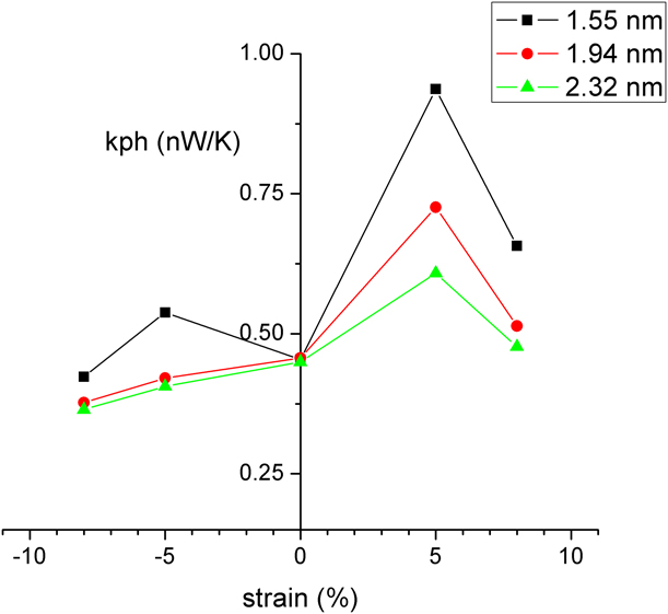
With the application of compressive strain, the phonon thermal conductance is found to reduce as illustrated in Fig. 2. This can be attributed to the fact that there occurs an increase in the buckling parameter on compression, which results in unfavorable propagating phonons, causing an increase in phonon scattering and, thus, a decrease in thermal conductivity [Reference Wei, Xu, Wang and Zheng14]. With a further increase in the magnitude of the strain, the thermal conductivity gets reduced further.
Phonon thermal conductivity as a function of applied strain for 1.55, 1.94, and 2.32 nm porous ASiNRs.

However, there occurs an initial increase in the phonon thermal conductance when subjected to a tensile strain. This behavior is due to the initial buckled configuration. At smaller strains of the order of 5%, there occurs a slight flattening of the buckled configuration on stretching because of the bond rotation, resulting in an enhanced silicene in-plane stiffness, thereby favoring the propagation of phonons [Reference Pei, Zhang, Sha and Shenoy4, Reference Xie, Ouyang, Germaneau, Qin, Hu and Bao18]. However, for larger strains beyond 5%, the Si–Si bonds are severely stretched; as a consequence, silicene in-plane stiffness decreases and the phonon modes are softened because of the increase of lattice anharmonicity and, hence, a decrease in thermal conductivity [Reference Kara, Enriquez, Seitsonen, Voon, Vizzini, Aufray and Oughaddou2].
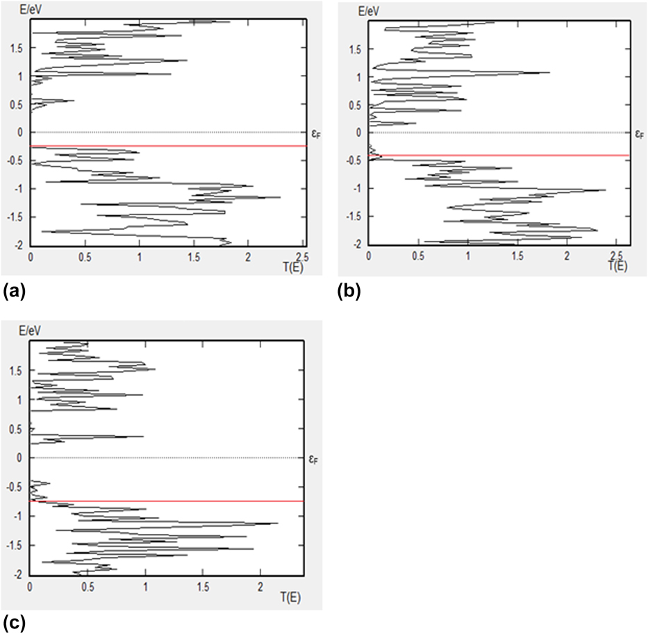
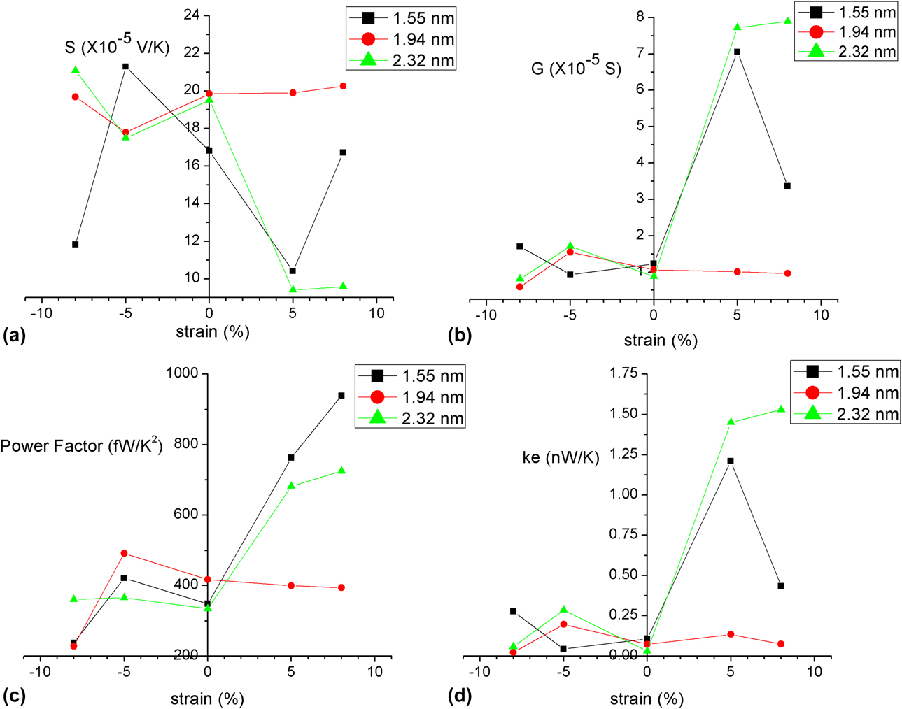
For attaining larger values of conductance which exhibits a direct dependence with ZT, the chemical potential should be shifted deep into the conduction band which in turn will reduce the E-µ term, resulting in a smaller Seebeck coefficient as predicted in Eq. (3). Therefore, the shape of the transmission spectra needs to be optimally controlled, which provides with a good compromise between the Seebeck coefficient and conductance [Reference Hossain, Al-Dirini, Hossain and Skafidas21]. Figures 3(a)–3(c) depict the transmission spectra due to electrons as a function of energy for 1.55, 1.94, and 2.32 nm pore diameter embedded in ASiNRs under a compressive strain of 5% for which a maximum figure of merit ZT is achieved. Here, the straight bold lines indicate the chemical potential at which peak ZT has been achieved, which is at −0.19, −0.40, and −0.74 eV for (a), (b), and (c), respectively. The variation of S, G, power factor (S 2G), and k e with the strain values for the structures are plotted in Figs. 4(a)–4(d).
(a)–(c) Electron transmission spectrum for 1.55, 1.94, and 2.32 nm porous ASiNRs at compression of 5% for which peak ZT is attained.

(a) Seebeck coefficient, (b) conductance, (c) power factor, and (d) electron thermal conductance as a function of strain for porous ASiNRs of 1.55, 1.94, and 2.32 nm.

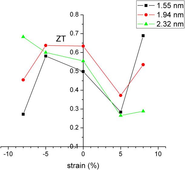
Figure 5 plots the strain dependence of the figure of merit ZT for the porous structures. The figure clearly demonstrates that a smaller uniaxial tensile deformation of up to 5% is not a suitable option for improving the thermoelectric performance. Also, except for a porous structure of 1.55 nm pore size where a tensile strain of 8% is showing some improvement of around 31%, it fails to do so for larger pore diameters. Therefore, smaller pores are observed to respond better to higher tensile deformation than the larger pores. On the other hand, even a compression of 5% is found to improve the thermoelectric figure of merit ZT for all structures irrespective of the pore size. Whereas at larger compression, the thermoelectric performance of bigger pores is better than smaller ones, thereby behaving differently from tensile deformation.
Overall figure of merit ZT as a function of applied strain for 1.55, 1.94, and 2.32 nm porous ASiNRs.

It is clear from the figure that ZT begins to decrease at larger compressive deformation for smaller pore sizes, whereas for a larger pore size of 2.32 nm, it gets improved by a factor of 23% as compared with its unstrained value. Thus, it can be concluded that the thermoelectric efficiency can be effectively modulated by the proper choice of tensile/compressive strain depending on the pore size. Hence, for smaller pore sizes, tensile strain is preferred, whereas for larger porous diameters, the compression is a suitable option.
Effect of temperature on thermoelectric performance
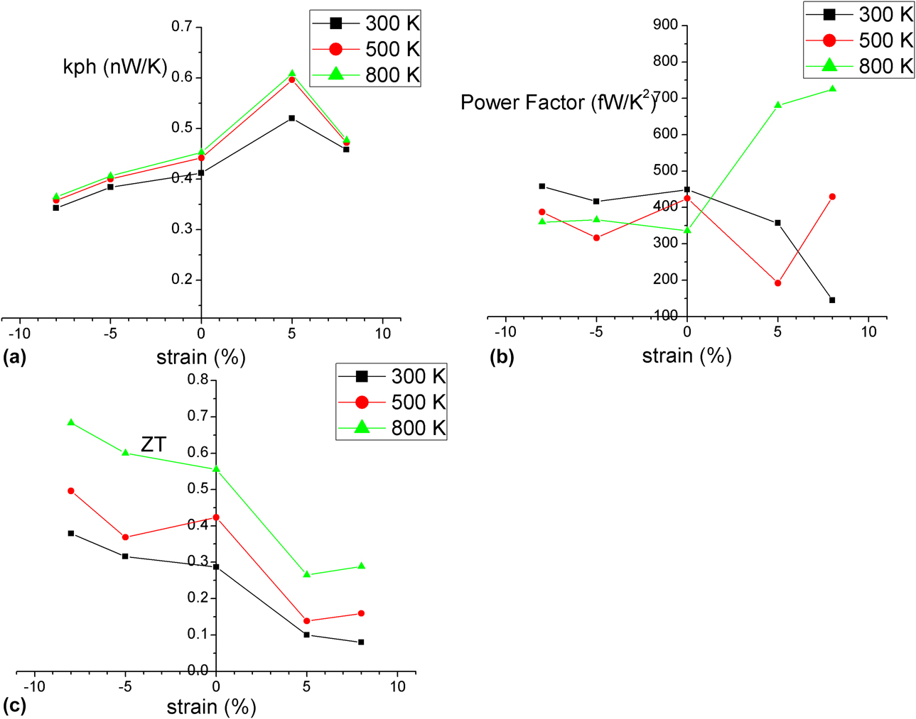
To investigate the effect of temperature on the thermoelectric properties of ASiNRs, the model of 2.32 nm pore diameter is simulated for three representative temperatures of 300, 500, and 800 K corresponding to low, intermediate, and high temperatures, respectively. The variation in k ph with respect to the applied strain is shown in Fig. 6(a). It clearly demonstrates that even at 300 and 500 K, its variation shows the similar trend as was observed earlier in Fig. 2 at 800 K. In addition, it is found to increase with the increase in temperature [Reference De Padova, Perfetti, Olivieri, Quaresima, Ottaviani and Le Lay6]. Figure 6(b) shows the variation of power factor at different temperatures. Also, it is observed that ZT dependence on strain as shown in Fig. 6(c) follows exactly the same variation as that for 800 K [Fig. 5], with the peak value of ZT increasing with the increase in temperature. Thus, it clearly concludes that a compression of 8% tends to give the most promising results irrespective of the choice of temperature and, hence, should be preferred. On concluding remarks, the tensile deformation fails to give any improvement in ZT at any choice of temperature, whereas the performance under compressive deformation goes on improving with the increase in the applied temperature. Figures 6(a) and 6(c) thus shows that for higher temperatures, the variation in k ph and ZT is more sensitive to strain because of the larger spread of  ${{\partial f} \over {\partial E}}$ which magnifies the changes to T(E) and band gap [Reference Yeo, Sullivan, Loh and Gan15]. The peak percentage decrease in k ph and increase in ZT for these temperatures on the application of compressive strain from 0 to ±8% are summarized in Table I.
(a) Phonon thermal conductance, (b) power factor, and (c) figure of merit ZT as a function of strain for 2.32 nm porous ASiNR subjected to low, intermediate, and high temperatures of 300, 500, and 800 K, respectively.

Peak percentage decrease in k ph and increase in ZT for the representative temperatures of 300, 500, and 800 K on the application of strain of the order of ±8%.

Effect of pore shape on thermoelectric properties
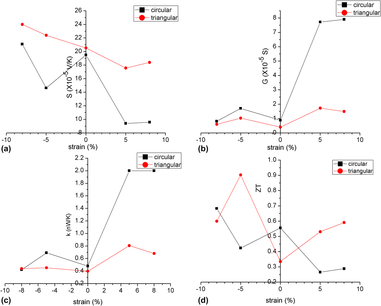
In this section, the circular-shaped nanostructure of 2.32 nm pore diameter where peak ZT ∼ 1 has been obtained is compared with the equivalent triangular-shaped pore of 3.15 nm side each involving the same number of removed atoms i.e., 70 in this case. Figure 7 illustrates the comparison between the thermoelectric coefficients of S, G, k ph, and ZT. It is hereby observed that the transport coefficients of S and G show a larger variation to the strain than the triangular one. It clearly depicts that the introduction of a tensile strain tends the circular-pored structure to a become better conductor of electricity [Fig. 7(b)], although at the cost of lower Seebeck coefficient [Fig. 7(a)]. Figure 7(c) depicts that the triangular pores offer smaller thermal conductance than their circular counterparts [Reference Romano and Grossman22] irrespective of the nature of strain. This is primarily due to the weaker interatomic interactions which occur because of the accumulation of inelastic deformation in the triangular pore [Reference Gong, Cui, Zhao, Sun and Ding23]. Figure 7(d) presents an interesting property that ZT of triangular pores is improved significantly over circular pores in the presence of strain. This remarkable enhancement of the thermoelectric figure of merit comes from the suppression of the thermal conductance effect and the improvement of Seebeck coefficient, outweighing the decreasing electrical conductance.
Shape-dependent behavior of (a) Seebeck coefficient, (b) conductance, (c) overall thermal conductance, and (d) figure of merit as a function of strain.

Conclusion
In conclusion, we have examined porous armchair silicene nanoribbons under uniaxial tension and compression, which reveals interesting features where electronic and phononic properties are strongly modified. The results conclude that the thermoelectric efficiency can be effectively modulated by the optimum choice of tensile/compressive strain depending on the pore size. For smaller pore sizes, tensile strain is preferred, whereas for larger porous diameters, the compression is a suitable option. In addition, tensile deformation fails to give any improvement in the figure of merit at any choice of temperature, whereas the performance under compressive deformation goes on improving with the increase in the applied temperature. In addition, triangular pores are proved to have better thermoelectric performance than their circular counterparts under the presence of strain. Hence, our findings indicate a theoretical framework for tailoring the functionality of silicon-based nanodevices via straining, which could be of interest to the designers and present promising applications in thermoelectric applications.
Methodology
In this study, the nanoribbons with different pore diameters have been studied as a model to improve the thermoelectric performance when subjected to a uniaxial tensile and compressive strain of 5 and 8% each. Also, the effect of the change in the pore shape has been examined. The parameter used for denoting the strain is  $\varepsilon = \left( {{L \over {{L_0}}} - 1} \right)$, where L (L 0) is the length (relaxed length) of the ribbon along the edges. The positive and negative signs of ε denote the tensile and compressive strain, respectively [Reference Yeo, Loh and Gan13].
The efficiency of a thermoelectric material is evaluated by the dimensionless figure of merit ZT = S 2GT/(k e + k ph), where G is the electrical conductance, S is the Seebeck coefficient, k e (k ph) is the thermal conductance contributed with electrons (phonons), and T is the average temperature. Therefore, an optimal thermoelectric material should possess high S, high G, and a low value of thermal conductance.
The quantum transport properties are investigated by the Extended Huckel theory (EHT) [Reference Stokbro, Peterson, Smidstrup, Blom, Ipsen and Kaasbjerg24, Reference Martins and Valves25] coupled with the nonequilibrium Green’s function method as implemented in the Virtual NanoLab-Atomistix Toolkit (ATK) software package (SYNOPSYS, USA). Within the EHT framework, the retarded Green function G R = (ES ov − H − ΣL − ΣR)−1, where E is the electron energy, H and S ov are the Hamiltonian and overlap matrix of the central region, respectively, which are calculated using Hoffman basis. Once the retarded Green’s function is obtained, the electron transmission function can be obtained through:
 $$T\left( E \right) = {\rm{Trace}}\left[ {{\Gamma _{\rm{R}}}\left( E \right){G^{\rm{R}}}\left( E \right){\Gamma _{\rm{L}}}\left( E \right){G^{{\rm{R}}\dag }}\left( E \right)} \right]\quad ,$$
where ΓL,R(E) = i(ΣL,R(E) – ΣL,R†(E)) describes the level broadening due to the coupling between the left/right electrodes and the central scattering region and ΣL,R(E) are the retarded self-energies for the electrodes. The mesh points in real space calculation of 1 × 1 × 100k points, mesh cut-off of 10 Hartree, and a temperature of 800 K are hereby considered.
From the investigation of T(E), Seebeck coefficient S, electrical conductance G, and electronic thermal conductance k e can be obtained under linear response approximation as [Reference Hossain, Al-Dirini, Hossain and Skafidas21]:
 $$G = {\left. {{I \over {\Delta V}}} \right|_{\Delta T = 0}} = {{\rm{e}}^2}{L_0}\quad ,$$
 $$S = {\left. {{{\Delta V} \over { - \Delta T}}} \right|_{I = 0}} = {{{L_1}} \over {{\rm{e}}T{L_0}}}\quad ,$$
 $${k_{\rm{e}}} = {\left. {{{{I_{\rm{Q}}}} \over {\Delta T}}} \right|_{IE = 0}} = {{{L_2} - {{L_1^2} \over {{L_0}}}} \over T}\quad ,$$
where
 $${L_n} = {2 \over h}\int {{\rm{d}}ET\left( E \right)\left( {{{ - \partial f} \over {\partial E}}} \right){{\left( {E - \mu } \right)}^n}} \quad ,$$
where L n is the Lorenz function, e is the charge of the electron, h is the Planck constant, μ is the chemical potential, T is the average temperature, and ∂f/∂E is the derivative of the Fermi function [f = 1 + exp ((E − μ)/k BT)−1] known as Fermi–Dirac distribution function.
To calculate the phonon thermal conductance, we used the Landauer approach [Reference Landauer26]:
 $${k_{{\rm{ph}}}} = {{{h^2}} \over {2\pi {k_{\rm{B}}}{T^2}}}\int {{\rm{d}}\omega {\omega ^2}{T_{{\rm{ph}}}}\left( \omega \right)} \left( {{{\partial n} \over {\partial \omega }}} \right)\quad .$$
For phonon transmission T ph(ω), H and S are substituted by a force constant matrix K and a diagonal matrix of atomic mass M, respectively. The term ∂n/∂ω is the derivative of the Bose–Einstein distribution for phonons. To calculate the force constant matrix for phonons, empirical Brenner potential was used. In this work, independent electron and phonon calculations have been performed while neglecting the electron–phonon interactions.