I. INTRODUCTION
RF MEMS switches are considered to be among the key components in mobile communication for the reconfiguration of filters, of antennas, and of front end modules. Low insertion loss (<1 dB), high isolation (>30 dB), fast response time (<50 µs), low actuation voltage (<10 V), low actuation power consumption (<1 µW), and long lifetime (>1 billion switch cycles) need to be achieved. The contact force is playing an important role for low contact resistance and insertion loss as well as for high reliability as stated in previous papers, e.g. [Reference Ma1, Reference Patel and Rebeiz2]. Adhesion forces, van der Waals bonds, metal bonds [Reference Jensen, Huang, Chow and Kurabayashi3], thin films of weakly conducting materials [Reference Majumder, McGruer, Adams, Zavracky, Morrison and Krim4], and contact necking [Reference Patton and Zabinski5] respectively ductile separation [Reference Du, Adams, McGruer and Etsion6] have been identified to be the main reasons for reliability issues in case of too low contact force or contact separation force. A strong contact separation force is necessary to prevent contact sticking [Reference Tringe, Wilson and Houston7]. Also Rebeiz et al. [Reference Rebeiz, Patel, Han, Ko and Ho8] state high contact and release forces as essential for reliable RF MEMS switches. Additionally, they mention that hermetic encapsulation of the contacts increases reliability.
This contribution reports on the analysis of metal–metal contacts of RF MEMS switches. A high-aspect-ratio fabrication sequence in combination with wafer level packaging is applied for fabrication of an RF MEMS switch with lateral motion. The MEMS switch presented in this work has a relatively large actuation electrode area. This leads to high actuation force even with an actuation voltage of 5 V in contrast to earlier presented switches with small actuation areas and thus high actuation voltages or even sophisticated actuation waveforms [Reference Liu, Tang, Agarwal and Alphones9–Reference Guo, McGruer and Adams11].
The focus of this contribution is on the contact behavior. It is shown how operation conditions such as actuation voltage, RF power, and DC bias influence the contact resistance. The power-handling capability and its influence on the contacts are also investigated. In addition to that, fundamental measurements on S-parameters and on switch time were conducted.
II. DESIGN AND ANALYSIS
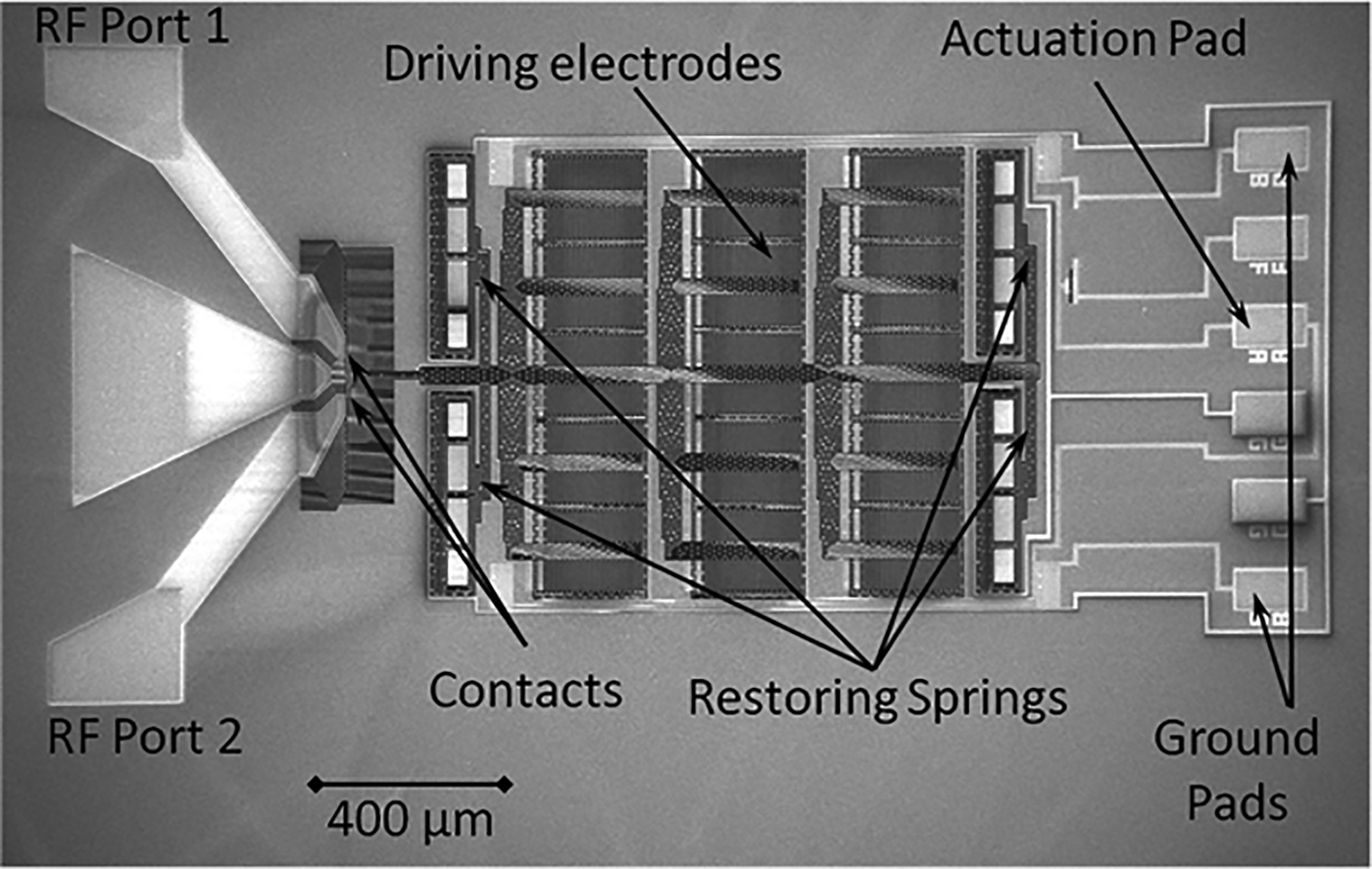
The RF MEMS switch is fabricated by a high-aspect-ratio fabrication sequence and wafer level sealing process and is reported earlier in [Reference Akiba12, Reference Kurth13]. Figure 1 shows a scanning electron microscopy (SEM) view of the chip. The driving electrodes in the middle of the picture are built up from hundreds of comb-shaped parallel plate capacitors. Each capacitor has one electrode fixed to the bulk and the other electrode attached to the movable, horizontally oriented push-rods and stiff vertical bars. Those parallel plate capacitors provide sufficient actuation force even with low actuation voltage of 5 V. The bond pads visible on the right-hand side are used for applying the actuation voltage, for ground potential, and for fabrication in-line test purposes. The bulk material is crystalline high resistive silicon with a resistivity of 3–5 kΩ cm. Deep reactive ion etching and isotropic release etching of the movable parts from the substrate are applied to form the fixed electrodes, the fixed contacts and the movable parts (Fig. 2).
SEM view of the RF MEMS switch, top view without glass cap.

Schematic view of the cross section of the switch (not to scale).
To achieve high actuation force and low switch time, the electrode gap and the contact gaps in the open state need to be smaller than the etching process would naturally permit. A gap reduction procedure that reduces the gap size is introduced as one of the last fabrication steps. Details are published within [Reference Kurth13].
Figure 3 shows that the concept of this series switch is based on a double series switch. It also shows the contact area and its coating by the contact metal (barrier/Au layer stack). A shadow mask and sputter deposition as the pre-last process step before wafer packaging are applied. The gold covers the top surface of the contacts and the very upper part of the sidewalls. Because of the limited lateral resolution of the contact metal deposition procedure, the contact material is spreading in a certain area around the contact bar and the contacts. To achieve an appropriate isolation the surface is interrupted by multiple etched grooves. A wafer level sealing process (0-level packaging) is applied for hermetic vacuum encapsulation at a chamber pressure of the bonding tool of 20 mbar. More details on the fabrication sequence are given by Akiba et al. [Reference Akiba12] and Kurth et al. [Reference Kurth13].
SEM views of the gold-plated contact area. (a) Overview and (b) the detailed view of the contact at left-hand side at the status before the gap reduction procedure.
III. RF PERFORMANCE AND SWITCH TIMES
The RF performance measurements (Fig. 4) were conducted using a vector network analyzer ZVA50 (Rohde & Schwarz) and Z-Probes (Cascade Microtech). A special fixture with additional ground pads beside of the chip was used to be compatible to Ground-Signal-Ground probes and to need no interface between the chip and the probes. The reference planes for calibration were located at the probe tips. The measured results indicate very high isolation of typically better than −35 dB and insertion loss below −0.6 dB in the frequency range up to 5 GHz (Fig. 4).
Measured results of isolation, insertion loss, and return loss of the switch.
Another important parameter is the switch time. The measurement was performed with a 50 Ω input at the oscilloscope (Tektronix) for impedance matching and to avoid signal reflections. To keep the contact current low for cold switching, the contact test voltage was adjusted to 40 mV only. It results in visible noise superimposed to the test signal. However, it is not influencing the accuracy of the switch time measurement. Figure 5 shows typical curves for step signal actuation voltage. The very low switch time of <10 µs proves the benefits of high electrostatic forces as well as high restoring forces. In addition to that the vacuum atmosphere in the packaged chip contributes to low switch times. Experiments showed that there is no significant difference of switch times before and after load tests of Section IV.
Diagram from the oscilloscope showing switch time: (a) switching-on procedure, (b) switching-off procedure. Blue line indicates the actuation voltage; cyan line indicates the voltage at the output of the switch.
A prior paper on the dynamic behavior of a horizontal actuated RF MEMS switch presented a specific actuation waveform that accelerates switch procedures [Reference Guo, McGruer and Adams11]. Since the present results were obtained with a step impulse, further improvements might be possible.
IV. CONTACT INVESTIGATION
The comb drives described in Section II lead to a high actuation force (~350 µN) at low actuation voltage of 5 V and allows for strong restoring springs (500 N/m) and high contact separation force of 100 µN per contact. The values of actuation force and spring constant were obtained from simulations.
From Fig. 3, it appears that the contacts have a length of 2 µm. The contact metal depth on the sidewall is also approximately 3 µm and determined by the technology procedure. Nevertheless, because of the roughness of the contact metal, the contact area that really leads the current is considered to be much smaller (Fig. 6). Only the outmost asperities of the both contacts come into touch to the counterpart and contribute to the current path. The current spreads on both sides of the asperities in the contact material. One consequence of the decreased contact area is an enlarged contact resistance.
Schematic view of the contacts and detrimental effects.
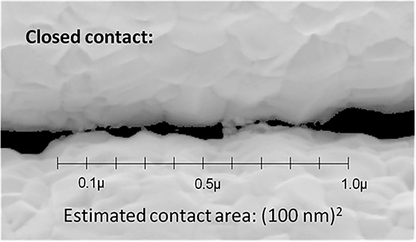
The SEM view from Fig. 7 shows contact spots at very tiny asperities at the contact in the closed state. The much lower contact force (~12 µN) was generated by reduced actuation voltage to demonstrate the situation. The total contact area is difficult to estimate, however, an area of much less than (100 nm)Reference Patel and Rebeiz2 can be estimated from Fig. 7.
SEM view of the contact area showing the asperities.
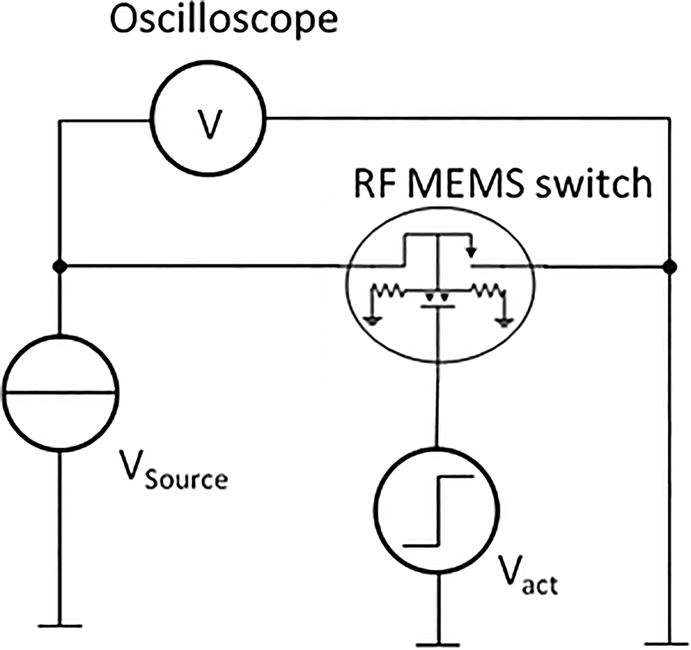
Hence, the specific resistivity of the contact material, the area of the asperities, and the number of asperities influence the resistance between the contacts. This is experimentally shown by an observation of the closing process with high time resolution (Fig. 8). The used measurement setup is displayed in Fig. 9. From the stepwise decreasing of the contact voltage at a given contact current of 6 mA during the contact closing procedure, one can derive that very few or even a single asperity contributes to the current path in case of the investigated contacts. This confirms measurements and derivations provided by Broue et al. [Reference Broue14]. It is assumed that each voltage step corresponds to an asperity that gets into contact and builds an additional current path. Possibly, it is combined with breaking of insulation layers on top of the asperities.
Diagram of measured contact voltage in the closing process with 6 mA contact current.
Schematic of the electric test circuit.
A) DC contact resistance
It is expected that the contact resistance depends on the actuation voltage because the actuation voltage determines the contact force. The area of the asperities increases with increased contact force and the contact resistance decreases. In addition, it may contribute to mechanical breaking of contamination layers at the contact metal surface. The number of zones that lead the electric current and the conducting area of each single asperity may be increased as a result. Figure 10 shows a typical contact behavior when the contact is closed for a first time and the actuation voltage is increased in a first part of the experiment and decreased in a second part. The stated force values were obtained by simulations and correspond to the force applied to each of the both contacts. The results confirm experiments conducted in [Reference Kwon15]. The contact starts the forming process with the weak contact force and shows a larger contact resistance. With increased actuation voltage, the contact force becomes larger and a higher number of asperities and a larger area contribute to the current path (higher and steep part of the curve within Fig. 10). This situation holds even when the actuation voltage is reduced in the second part of the experiment. An important property of the structure related to this issue is the elasticity of contact beams (Fig. 3), that compensates the differences in the contact gap between both contacts within a chip that may occur by technology tolerances. If one contact is closed earlier than the other, the elasticity of the contact beams allows for further travel of the push rod to close the other contact subsequently. This also enables remaining contact, even if the actuation voltage decreases subsequently and does not fall below a certain value (lower part of the curve within Fig. 10).
Diagram of measured contact resistance when varying the actuation voltage from the pull in voltage to higher values and subsequently to lower voltage down to release voltage.
Another experiment investigates the contact resistance and its dependency on the period of time in the closed state. Therefore, the previous measurement setup (Fig. 9) was used. The current was controlled by the source and from this current and the voltage measured across both contacts the resistance was calculated.
Figure 11 shows the results for different contact currents. We derive that mechanical creep is causing the fluctuation of the contact resistance. In this case (below 30 min), the heat introduced by higher currents flowing through the contacts has negligible influence on the creep process compared to mechanical stress.
Diagram of contact resistance over time, showing the small impact of creep on the contact resistance for different power.
B) Power handling
The power-handling capability was measured by applying a 1 GHz signal of variable power on the contacts while measuring the output power of the RF MEMS switch that have been assembled on a printed circuit board. During the tests, the RF MEMS switches were actuated by their nominal actuation voltage (V act = 5 V) before the RF power was enabled (cold switching). The RF power was increased in 1 dBm steps and held for approximately 5 s in each step. The RF power was reduced to approximately −20 dBm and the switch was tested by de-actuating and actuating while observing the output power. The regular function of the switch was checked during this simple on/off test.
The results within Fig. 12 show a linear behavior within the power range of up to 37 dBm input power at the RF MEMS switch. A compression would lead to increased insertion loss and is not observed.
Diagram of insertion loss of different RF MEMS switches at varying input power, measurement values.
The scatter parameters were measured before and after the test (Fig. 13). There is no significant change of isolation and reflection loss occurring. The insertion loss is decreased in comparison to the loss before the load test. It is assumed that the high power increased the current carrying area of the asperities of the contact.
Diagram of measured scatter parameters before and after power handling.
V. CONCLUSION
The experimental results show that the current path is supported by only a few asperities. Furthermore, the dependency of the contact resistance on the contact force was clearly observed during closing procedure, when growing contact force was applied. After subsequent decreased contact force the contact resistance remains low accounting for mechanical flattened asperities. Additionally, it is obtained by the DC measurement with contact currents up to 10 mA and by loading the contacts with RF power up to 37 dBm that metal softening by Joule heating does not play the dominant role in contact formation, when Au contacts are operated in dry vacuum atmosphere. Finally, the authors demonstrated that transmission of high-power signals of up to 37 dBm does not degrade the RF performance of the proposed switch. The work shows that the contact force needs to be high in order to obtain suitable contact resistances. The contact separation force has to ensure contact breaking after exposure to high-power signals. Therefore it needs to be high as well.
ACKNOWLEDGEMENTS
The authors would like to acknowledge the financial support by the German Federal Ministry of Education and Research (contract no. 03IS2011 K) and by Sony Corporation and are very grateful for valuable discussion with Dr. Koichi Ikeda and Akira Akiba.
 Markus Gaitzsch received his B.Sc. and M.Sc. degrees both in Electro Engineering from the Chemnitz University of Technology in 2007 and 2013, respectively. He works at the Chemnitz University of Technology at the Center for Microtechnologies. His working fields are RF MEMS, antennas, material characterization, and general measurement tasks.
 Steffen Kurth received his Dipl.-Ing. degree in Electrical Engineering and the Dr.-Ing. degree in MEMS modeling and experimental characterization from the Chemnitz University of Technology, Chemnitz, Germany, in 1991 and 1995, respectively. He was a lecturer with the Chemnitz University of Technology and supervised more than 30 graduate students for Diploma and Dr.-Ing. degrees. Since 2001, he has been with the Fraunhofer Institute for Reliability and Microintegration and the Fraunhofer Institute for Electronic Nano Systems (ENAS), Chemnitz, and has been active in the fields of design and test of MEMS components, such as accelerometers, vacuum pressure sensors, scanning mirrors, tunable infrared filters, and other micro-optoelectromechanical system components. He is currently leading the MEMS Test Group, Fraunhofer ENAS, managing several joint research and development projects. His current research interests include the development of micro- and nanostructured components for micro-optoelectromechanical systems and radio-frequency MEMSs.
 Sven Voigt received his Dipl.-Ing. degree in Electrical Engineering from the Chemnitz University of Technology, Germany, in 2007. Thereafter, he worked at the Chemnitz University in the field of printed organic transistors and RF MEMS/NEMS devices. In 2013, he joined the Fraunhofer Institute for Electronic Nano Systems, where he continues to focus on RF MEMS/NEMS devices and sensor systems.
 Sven Haas received his Dipl.-Ing. degree from the Technische Universität Bergakademie Freiberg, Germany in 2011. He joined the Center for Microtechnologies of the Chemnitz University of Technology in 2011. His research interests are design and fabrication of high-aspect-ratio microstructures as well as CMOS-based transducers.
 Thomas Gessner studied physics and received his degree in Physics in 1979,Ph.D. degree in 1983 from the Dresden University of Technology and the Dr.-Ing. habil. degree from the Chemnitz University of Technology in 1989. Since 1991, he has been the Director of the Center for Microtechnologies and since 1993, he has been the Professor for Microtechnology, both at the Chemnitz University of Technology. Moreover, Prof. Gessner has been the founder and director of the Fraunhofer Institute for Electronic Nano Systems ENAS since 2008. He is author or co-author of more than 800 publications and 38 patent applications in microelectronics and micro systems technologies.