I. INTRODUCTION
Millimeter-wave phase shifters are important components for a wide scope of applications such as automotive radars, high-capacity communication systems, satellite communication, etc. Existing millimeter-wave phase shifters change the phase by adjusting either the geometrical parameters of the device (e.g. changing the length of a transmission line using switches), or material properties of its components (e.g. by applying magnetic or electric field). Phase shifters based on switched networks and distributed transmission lines may be inconvenient, e.g. in phased arrays due to their relatively large size. Besides they provide with a discrete phase shift only, and of no more than 4.25 bits at frequencies above 60 GHz, e.g. [Reference Hung, Dussopt and Rebeiz1–Reference Somjit, Stemme and Oberhammer3], which restricts their usability. Using materials with controllable parameters (e.g. ferroelectrics) for phase shifter usually results in high insertion loss at millimeter wavelength frequencies, e.g. 10 dB for a continuous phase shift up to 220° at 60 GHz [Reference Kozyrev4]. That is why we propose an approach that combines micro-electromechanical systems (MEMS) fabrication technology with the concept of artificial electromagnetic surfaces for realization of analog-type millimeter-wave phase shifters. MEMS technology allows one to miniaturize electronic components, reduce their cost in batch production, and effectively compete with semiconductor and ferroelectric technology in terms of losses. Combined with the artificial electromagnetic surfaces, MEMS varactors enable tunability of unique engineered properties of these surfaces. Previously, we proposed the design of a novel MEMS tunable high-impedance surface (HIS), analyzed its electromagnetic properties analytically and numerically, studied possible applications, and fabricated and measured several non-tunable prototypes, as well as tunable MEMS capacitors [Reference Chicherin, Dudorov, Lioubtchenko, Ovchinnikov, Tretyakov and Räisänen5–Reference Chicherin12]. In this work we present for the first time the measurement results of the MEMS-based HIS that is tunable in an analog way and is employed in an analog-type phase shifter.
II. MEMS TUNABLE HIS
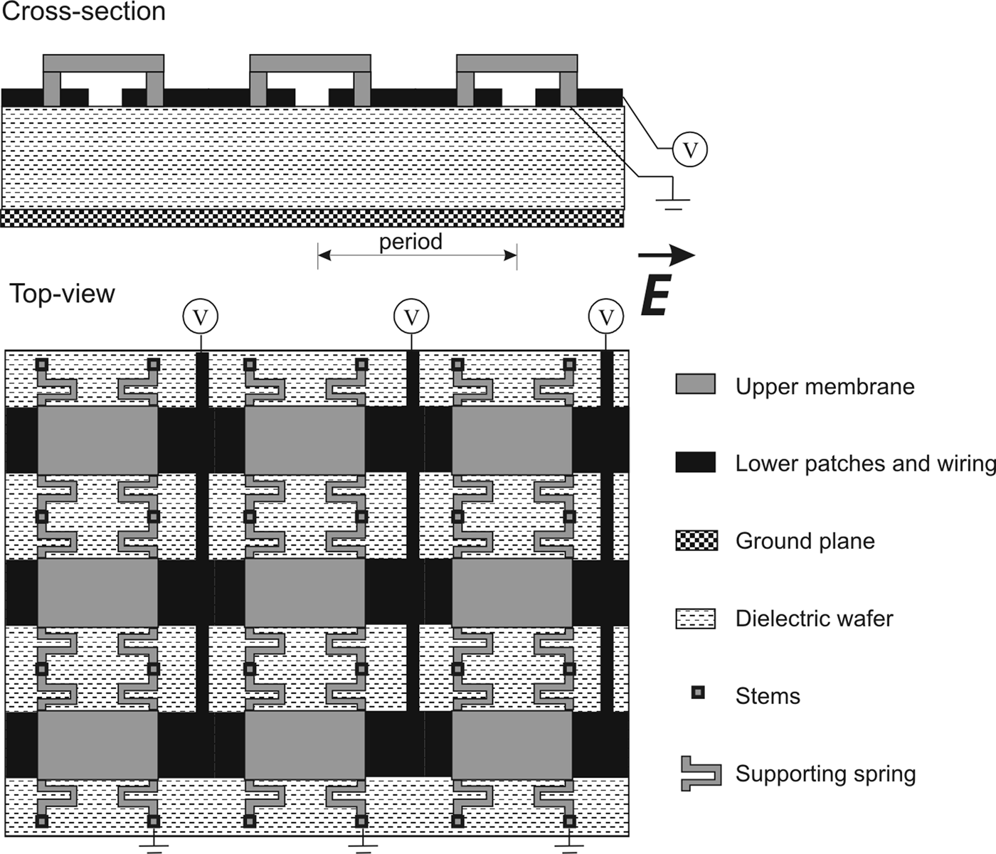
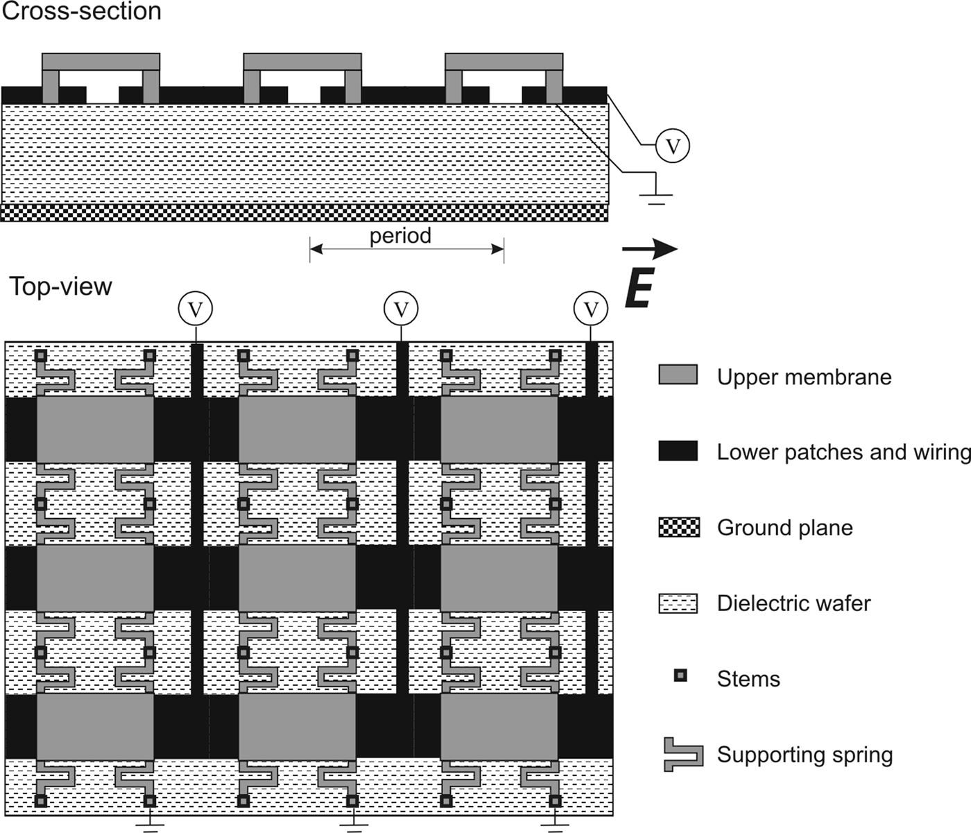
Conventional HIS [Reference Sievenpiper13] consists of a capacitive two-dimensional periodic grid of electrically small metal patches placed on a thin dielectric substrate with a ground plane. As the period of the structure is much smaller than the wavelength of the field above it, an effective surface impedance model can be used to analyze the electromagnetic behavior of the HIS. The grid of metal patches provides a capacitive response to the incident electromagnetic field, whereas the thin grounded dielectric substrate provides an inductive response. As a result, the HIS is a resonant structure, and at the resonance frequency the effective input impedance becomes very high, and the phase of the reflection coefficient changes from 180 to 0°. The HIS was proposed for such applications as an improvement of antenna radiation parameters, suppression of the surface waves, and leaky wave antennas [Reference Sievenpiper, Zhang, Broas, Alexpolous and Yablonovitch14, Reference Sievenpiper15]. Tunable HIS controlled with diode varactors and InP quantum barrier varactors were utilized for demonstrating beam steering [Reference Sievenpiper16] and metal waveguide phase shifting [Reference Higgins, Xin, Sailer and Rosker17], respectively. However, at W-band these tunable elements exhibit high losses. That is why we proposed to employ MEMS varactors for reconfiguring the HIS [Reference Chicherin, Dudorov, Lioubtchenko, Ovchinnikov, Tretyakov and Räisänen5]. The MEMS tunable HIS, consequently, consists of a two-dimensional periodic arrangement of MEMS varactors placed on a grounded Si substrate with a period much smaller than the wavelength of a field above the HIS, see Fig. 1.
MEMS tunable HIS (part of a large periodic arrangement is shown).
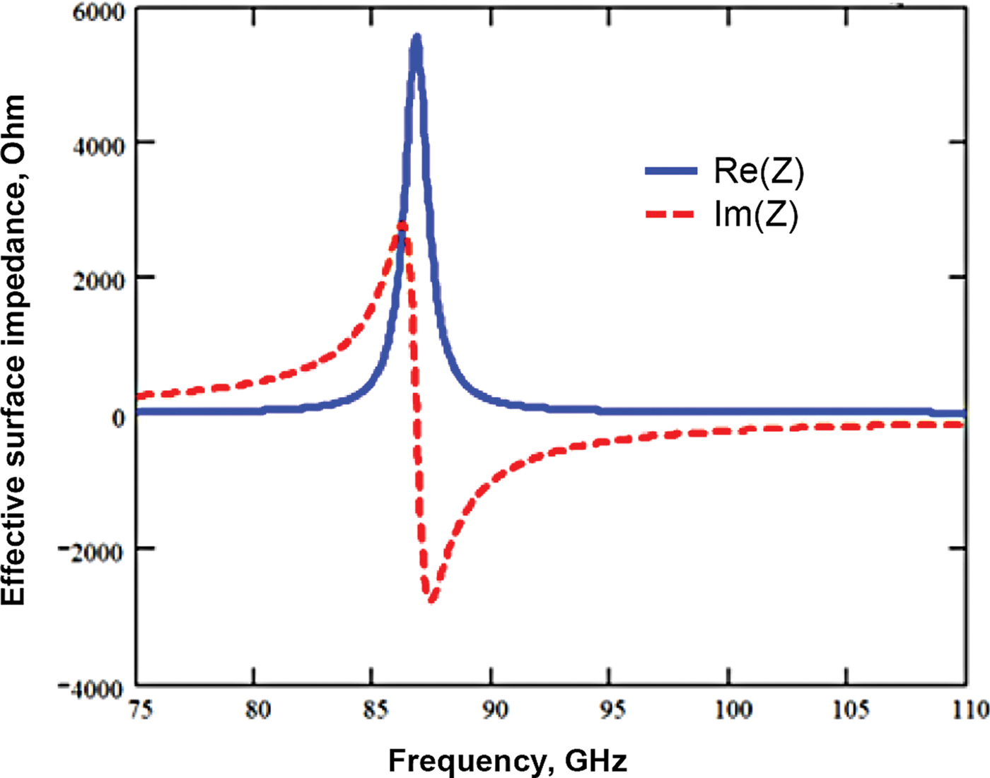
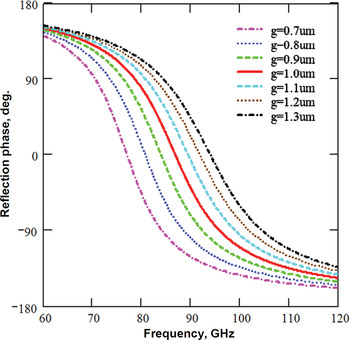
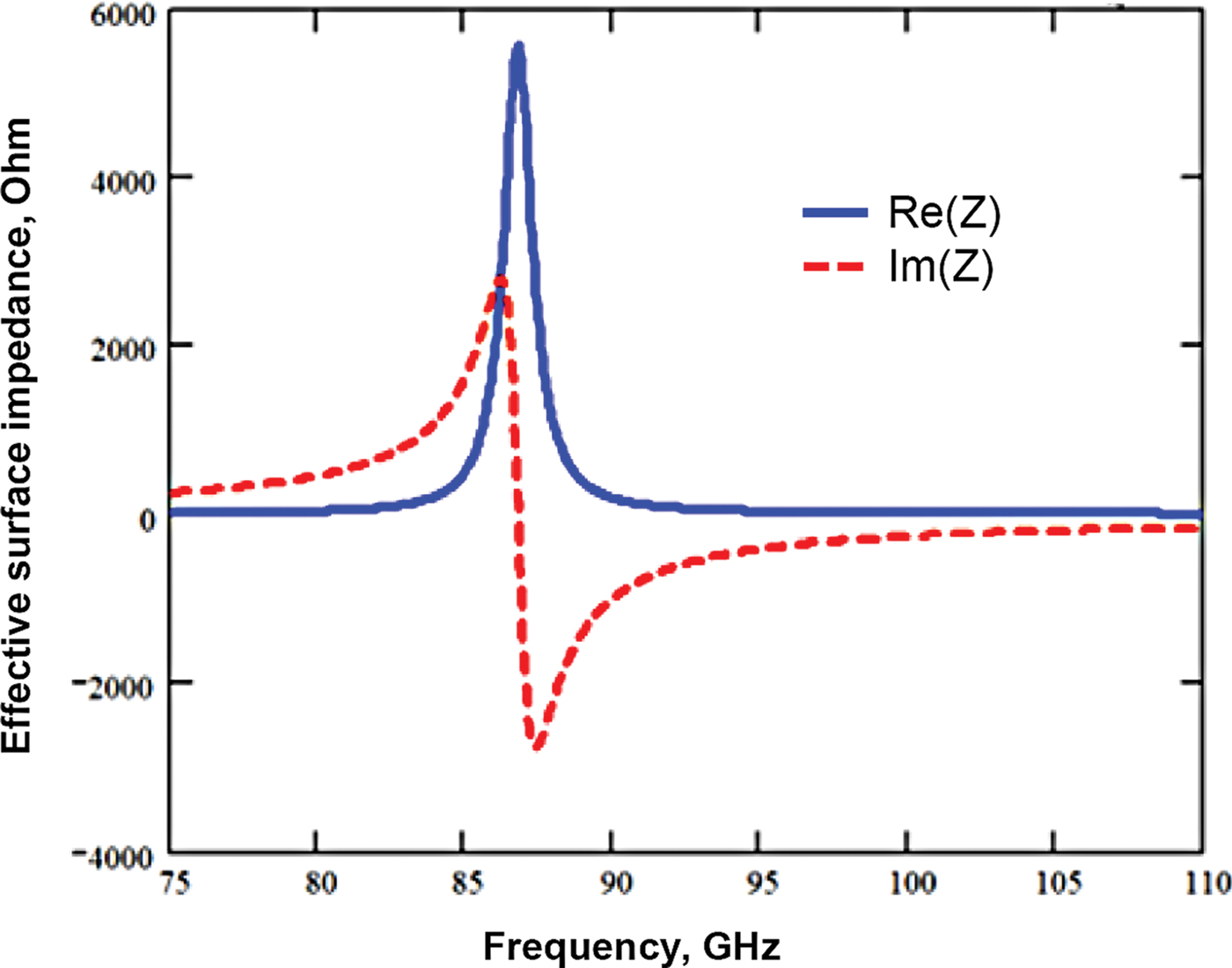
The bias voltages applied to a MEMS varactor controls its capacitance value by changing the gap between the upper membrane and lower patch, affecting accordingly the effective input impedance of the whole structure. Fig. 2 shows frequency dependence of the effective surface impedance of the HIS. The phase of the reflection coefficient of the MEMS tunable HIS for different values of the gap between the upper membranes and lower patches is given in Fig. 3.
Real and imaginary part of the effective surface impedance of the MEMS based HIS, calculated.
Reflection phase of the MEMS tunable HIS for different values of the gap g between the upper membranes and lower patches, calculated.

III. ANALOG-TYPE PHASE SHIFTER
A) Design
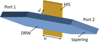
The MEMS tunable HIS can be used to control the phase factor of the propagation constant of a dielectric rod waveguide (DRW) placed adjacent to the HIS at a distance d, see Fig. 4, forming thus an analog-type phase shifter as soon as the bias voltage changes the capacitance value of the MEMS varactors gradually. The value of the phase shift is proportional to the length w of the HIS. The device can be used as a dielectric rod antenna with integrated phase shifter if the wave radiates to the free space from Port 2. Furthermore, a phase array antenna can be formed by placing n DRW one above another and adjacent to n HIS controlled individually. These HIS can be fabricated on a single chip will dramatically reduce complexity and, consequently, the cost of the array antenna.
Phase shifter based on a MEMS tunable HIS of width w adjacent to a DRW at a distance d (3D view).

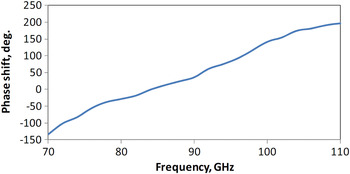
Simulation results of the phase shift of the DRW with adjacent MEMS tunable HIS, when the gap of MEMS varactors changes from 2 to 1.2 µm is shown in Fig. 5, demonstrating promising phase shifting potential. Previously we also fabricated a non-tunable prototype of the MEMS-based HIS for the DRW phase shifter, measuring S-parameters with HIS and a copper plate adjacent to the DRW for assessing the maximum achievable phase shift while tuning the structure from a high-impedance state to a low-impedance state [Reference Chicherin12].
Simulated phase shift of the DRW with adjacent MEMS tunable HIS.

B) Fabrication
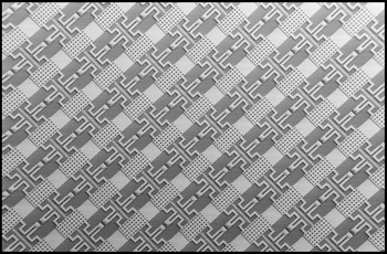
A prototype of the MEMS tunable HIS with 24 × 120 MEMS varactors placed on a silicon substrate with the period of 250 µm and total size of 6 × 30 mm2 has been fabricated, see Fig. 6. All varactors are connected by bias voltage lines to two contact pads.
SEM image of the fabricated prototype of MEMS tunable HIS.

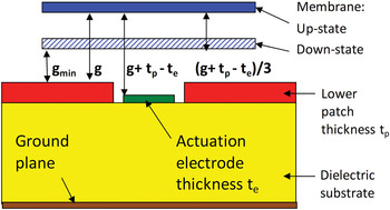
In order to increase the tunability range of the MEMS varactors, special actuation electrodes of the thickness smaller than the thickness of the lower patches are introduced into the HIS model, which do not affect performance of the HIS according to the both analytical and numerical analysis. For a simple parallel plate MEMS varactor, the gap between the upper membrane and lower patch can be decreased continuously by the bias voltage applied to them only by one-third of its initial value g to g min = g × 2/3 [Reference Rebeiz18]. If more bias voltage is applied, the membrane collapses to the lower patch, consequently the maximum achievable capacitance ratio is 1.5. On the other hand, if the additional actuation electrode of small thickness t e comparing with the thickness of the lower patches t p is used for bias voltage, see Fig. 7, then the rule of two-third is applied for the larger gap g + t p − t e, and consequently the maximum achievable capacitance ratio is
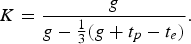
For g = 1 µm, t p = 1 µm, and t e = 0.2 µm, the capacitance ratio is 2.5.
Schematic overview of a single cell of the MEMS-based HIS for extended tuning range (side view).

C) Measurements
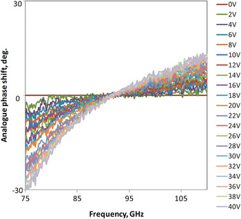
The MEMS tunable HIS is placed adjacent to the silicon DRW matched to WR-10 waveports of a vector network analyzer for measuring S-parameters. The bias voltage from 0 to 40 V is applied to all MEMS varactors simultaneously. An analog-type phase shift is detected at Port 2 of the DRW, see Fig. 8, where the phase of S 21 of biased phase shifter is referenced to the S 21 at 0 V. The measured frequency dependence of the phase shift at, e.g. 40 V bias voltage, corresponds to the simulated results, see Fig. 5.
Measured analog-type phase shift of the DRW with adjacent MEMS tunable HIS.

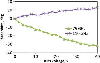
Dependence of the phase shift on the bias voltage is shown in Fig. 9 for 75 and 110 GHz, where the value of the phase shift is largest on the measured frequency range. The phase changes gradually from 0 to 13 and −32°. Larger phase shift value can be expected with higher bias voltage, and in case the HIS is optimized so that the minimum phase shift would appear, e.g. at 110 GHz.
Measured dependence of the phase shift on the bias voltage.

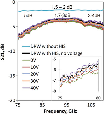
The S 21 of the DRW and DRW with adjacent HIS is given in Fig. 10, showing that the insertion loss of MEMS tunable HIS as a phase shifting element is between 3 and 5 dB. Second fabricated prototype, showing larger phase shift of up to 70°, exhibited higher insertion loss. The losses can be decreased by optimized fabrication procedure, choosing better material of the DRW and improving matching of DRW to the WR-10 ports of the VNA. It has been shown that insertion loss of a DRW matched to WR-10 can be as low as 0.4 dB [Reference Lioubtchenko, Dudorov, Mallat, Tuovinen and Räisänen19].
Measured insertion loss of the phase shifter.

IV. CONCLUSION
We have designed, manufactured, and measured an analog-type millimeter-wave phase shifters. The phase shifter comprises of a MEMS tunable HIS placed adjacent to a DRW. The analog-type phase shift of up to −32° has been demonstrated at 75 GHz by applying bias voltages from 0 to 40 V. Both the maximum phase shift value and the insertion loss can be improved by optimizing the design of the structure and the fabrication procedure. The proposed phase shifter can be used in a phase array antenna for millimeter-wave applications.
ACKNOWLEDGEMENTS
The research leading to these results has received funding from the European Community's Seventh Framework Programme (FP7/2007–2013) under grant agreement n° 224197 and from the Academy of Finland under the Center of Excellence in Research Programme, and was carried out in the frame of FP7 project TUMESA (MEMS Tuneable Metamaterials for Smart Wireless Applications, 2008–2011).
 Dmitry Chicherin received the B.Sc. (Phys.) and M.Sc. (Phys.) degree, both with honors, from Saint Petersburg State University, Russia in 1996 and 1998, respectively, and a postgraduate Lic.Sc. (Tech.) degree in ECE from Helsinki University of Technology, Finland in 2005. He has held visiting scientist positions at Université Joseph Fourier, Grenoble, France in 1997 and 1999–2000, and at Helsinki University of Technology Laboratory of Computational Engineering in 2001. He joined the Radio Laboratory, TKK – Helsinki University of Technology (currently Department of Radio Science and Engineering, Aalto University) in 2003 as a researcher. He was Project Manager and person in charge of scientific and technical aspects of FP7 project TUMESA (MEMS Tuneable Metamaterials for Smart Wireless Applications, 2008–2011) and also Work Packages leader in the international NORDITE-SARFA I and II projects (RF MEMS Steerable Antennas for Automotive Radar and Future Wireless Applications, 2006–2007 and 2008–2010). He is currently pursuing his Ph.D. degree on MEMS tunable high-impedance surface for millimeter-wave beam steering, whereas working as Research Liaison Officer at Aalto University, Finland.
 Mikael Sterner was born in Stockholm, Sweden, in 1981. He received the M.Sc. degree in engineering physics from KTH Royal Institute of Technology, Stockholm, Sweden, in 2006. He has been working toward the Ph.D. degree in microsystems technology at the Microsystem Technology Lab at KTH since 2006. His main research fields are RF MEMS switches and microwave MEMS tunable high-impedance surfaces.
 Dmitri Lioubtchenko was born in Gorky, Russia, in 1971. He received the B.S. and M.S. degrees and the Ph.D. degree in applied physics and mathematics from Moscow Institute of Physics and Technology, in 1993, 1994, and 1998, respectively. From 1994 to 1997, he was a Researcher in the Institute of Radio Engineering and Electronics, Russian Academy of Sciences, Moscow. From 1997 to 1998, he was a visiting researcher at the University of Liverpool, UK. Since 1998, he has been working at the Department of Radio Science and Engineering, Aalto University (formerly Radio Laboratory, TKK – Helsinki University of Technology), Finland, where he is currently an Academy Research Fellow. His research interests and experience cover various topics including investigations of new materials for millimeter-wave, microwave, and optoelectronic applications particularly, on the development of active and passive dielectric waveguides for the frequency above 100 GHz.
 Joachim Oberhammer born in Italy in 1976, received his M.Sc. degree in electrical engineering from Graz University of Technology, Austria, in 2000. He was working with automotive sensor electronics and RFID systems at Graz University of Technology and Vienna University of Technology, Austria, before he joined the Microsystem Technology Laboratory at KTH Royal Institute of Technology in Stockholm, Sweden. There, he received his Ph.D. degree in 2004 for his work on RF MEMS switches and microsystem packaging. After having been a post-doctoral research fellow at Nanyang Technological University, Singapore, he returned to the Royal Institute of Technology in 2005, attending an Assistant Professor position. In 2007, Dr. Oberhammer became an Associate Professor at the Royal Institute of Technology where he is heading a research team with activities in RF and microwave MEMS. In 2007, he was a research consultant at Nanyang Technological University, Singapore, and in 2008 he spent 7 months as a guest researcher at Kyoto University, Japan. He is the author and co-author of more than 60 reviewed research papers and holds four patents. In 2004 he got an Ericsson Research Foundation Award and in 2007 a grant by the Swedish Innovation Bridge, respectively. In 2008 he received a visiting-researcher scholarship from the Japanese Society for the Promotion of Science. The research work he is heading received the Best Paper Award at the IEEE European Microwave Integrated Circuit Conference in 2009, a Best Student Paper Award at IEEE Asia-Pacific Microwave Conference 2010, and Graduate Fellowships of the IEEE Microwave Theory and Techniques Society (MTT-S) both in 2010 and 2011. He served as TPRC member of IEEE Transducers 2009, IEEE International Microwave Symposium 2010 and 2011, and IEEE Micro Electro Mechanical Systems 2011. Dr. Oberhammer is Steering Group member of the IEEE MTT-S and AP-S Chapters Sweden since 2009.
 Antti V. Räisänen received the Doctor of Science (Tech.) degree in electrical engineering from the Helsinki University of Technology (TKK) (now Aalto University), Espoo, Finland, in 1981. In 1989, he became a Professor Chair of Radio Engineering with TKK, after holding the same position pro tem in 1985 and 1987–1989. He has been a Visiting Scientist and Professor with the Five College Radio Astronomy Observatory (FCRAO) and University of Massachusetts at Amherst (1978–1979, 1980, 1981), Chalmers University of Technology, Göteborg, Sweden (1983), University of California at Berkeley (1984–1985), Jet Propulsion Laboratory (JPL) and California Institute of Technology, Pasadena (1992–1993), and the Paris Observatory and University of Paris 6, Paris, France (2001–2002). He currently supervises research in millimeter-wave components, antennas, receivers, microwave measurements, etc. with the School of Electrical Engineering, Aalto University, Department of Radio Science and Engineering and Millimetre Wave Laboratory of Finland – ESA External Laboratory (MilliLab). The Center of Smart Radios and Wireless Research (SMARAD), which he leads at Aalto University, has obtained the national status of Center of Excellence (CoE) in Research in 2002–2007 and 2008–2013. He is currently Head of the Department of Radio Science and Engineering, Aalto University. In 1997, he was elected the Vice-Rector of TKK (1997–2000). He has authored or coauthored over 400 scientific or technical papers and six books, e.g., Radio Engineering for Wireless Communication and Sensor Applications (Artech House, 2003). Dr. Räisänen has been a Fellow of IEEE since 1994 and a Fellow of the Antenna Measurement Techniques Association (AMTA) since 2008. He has been conference chairman of several international microwave and millimeter-wave conferences including the 1992 European Microwave Conference. He was an associate editor of the IEEE Transactions on Microwave Theory and Techniques (2002–2005). He is a member of the Board of Directors of the European Microwave Association (EuMA) (2006–2011). He is currently chair of the Board of Directors, MilliLab. He was the recipient of the AMTA Distinguished Achievement Award in 2009.