Introduction
In recent years, there is a tendency to miniaturize the electronic devices for portability. As a result, antenna plays a crucial part in total volume of the package, so reduced antenna size is necessary. In this era faster data transmission has become mandatory for day-to-day activities like video conferencing, gaming, etc. which is partially fulfilled by ultra-wide band technology. In 2002, the F.C.C standardized 3.10–10.60 GHz band for commercial UWB purposes [1], after which the industry and academics have executed several research attempts. Planar printed monopoles are surely better to operate in UWB gadgets [Reference Azim, Mobashsher and Islam2–Reference Midya, Bhattacharjee and Mitra5] for producing broader bandwidth and good control. They also provide benefit in terms of degradation of the radiation pattern making it suitable candidate for pulse based communication systems such as UWB. UWB devices experience a problem based on the spectrum sharing with slender bands of IEEE 802.11a WLAN, HIPERLAN/2 operating in the range of 5.15–5.35 GHz and 5.725–5.825 GHz, respectively [Reference Chakraborty, Kundu, Chowdhury and Bhattacharjee6]. These narrower bands cause potential interference with ultra-wide bands lowering the performance of the set up. One solution is using filters with stop band criterion against certain frequency band. In the contrary, antennas incorporated with additional filter circuitry design are more complex and expensive. The most cost-effective way is by embedding slots in patch and ground plane [Reference Seo, Jung, Lee and Lim7–Reference Bhattacharya, Roy, Chowdhury and Bhattacharjee10] or by adding parasitic strips [Reference Huang, Huang and Yang11]. Lui et al. [Reference Lui, Cheng and Zhu12] used parasitic open-circuit stub to achieve frequency notch feature. Dual band split ring resonators (SRRs) is used in [Reference Safia O, Nedil, Talbi and Hettak13] for achieving dual notched characteristics while parasitic slits are implemented by Ye et al. [Reference Ye and Chu14] to achieve dual notch effect. Mukherjee et al. [Reference Mukherjee, Guha, Roy, Das, Banerjee, Aich and Mukherjee15] designed a T-shaped slotted antenna accompanied with inverted U-slot resonator inside feed line and symmetrical pair of slits in ground plane, while in [Reference Salamin, Ali and Zugari16], dual notch is observed by implementing dumbbell-shaped slot in the patch and in the ground structure as DGS. In [Reference Zeng, Zhang, Zhang and Zhao17] dual notch is achieved by introducing complementary split ring resonator (CSRR) in the hexagonal patch. Triple notch characteristics are also attained by using both CSRR and SRR as suggested by Yadav et al. [Reference Yadav, Agrawal and Yadav18] and Vendik et al. [Reference Vendik, Rusakov, Kanjanasit, Hong and Filonov19] achieved band-notch characteristics by incorporating electric ring resonator underneath the CPW structure. Similarly, Peddakrishna and Khan [Reference Peddakrishna and Khan20] recommended π-shaped slot in radiator accompanied by electromagnetic band gap structures to achieve duplex notch. An integrated GSM–UWB Fibonacci-shaped structure was introduced in [Reference Srivastava, Kumar, Kanaujia, Dwari, Verma, Esselle and Mittra21] with slots in feed line and ground plane to produce triple notch. Overlapping between the feedline and back resonator can give stop band characteristics as proposed by [Reference Das, Acharjee and Mandal22] or by using a parallel resonating parallel strip [Reference Yang, Jingjian and Naichang23]. Triple notch at Wi-Max/C band, WLAN and uplink-downlink X-band is generated by Bhusal and Labade [Reference Bhusal and Labade24] with the help of different shaped slits and parasitic stubs in the patch. Reconfigurable notch features are also attained by Orugu and Moses [Reference Orugu and Moses25] with the help of PIN diodes.
Here in a compact circular antenna is outlined by inserting a microstrip slot line transition with an Archimedean spiral slot in radiating patch section and one open-ended ground slot to achieve triple notch characteristics ranging from 3.49–4.41 GHz, 4.82–5.31 GHz to 8.50–9.30 GHz. These Archimedean spiral structures have been used by Lee et al. [Reference Lee, Yang and Cho26], Zhu et al. [Reference Zhu, Gao, Ho, Abd-Alhameed, See, Li and Xu27], Zhang and Brown [Reference Zhang and Brown28], Mashaal et al. [Reference Mashaal, Rahim, Abdulrahman, Sabran, Rani and Hall29] and Rao [Reference Rao30] as they provide an added advantage of improved return loss. Simulations are performed using IE3D Zeland software and various antenna design parameters are analyzed in detail from the parametric studies.
Antenna design and simulation
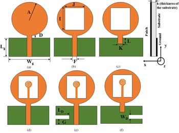
At first a circular monopole antenna is sketched on a flame resistant FR-4 material (ɛr = 4.4) of radius (A) = 12.0 mm and substrate thickness (h) = 1.60 mm. The reference antenna is symbolized as Antenna 1 fed by a 50 Ω line having feed width of (F) = 3.0 mm for better impedance matching depicted in Fig. 1(a). The ground plane of the overall antenna structure has a dimension of 24.00 × 14.50 mm2. Further a rectangle of dimension 15.00 mm × 11.00 mm is etched out on the patch as well as open-ended rectangular slit in the ground plane just underneath the feed as defected ground structure (DGS). This antenna is denoted as Antenna 2 whose top and back view is displayed in Figs 1(b) and 1(c), respectively. In the next step, a spiral slot in the strip line is embedded in the patch to cut off the WLAN (5.2 GHz) band as depicted in Fig. 1(d) and referred to as Antenna 3.
(a) Antenna 1 (reference antenna), (b) antenna 2 (top view), (c) antenna 2 (rear view) (d) antenna 3 (with spiral shaped slot), (e) antenna 4 (front view) and (f) antenna 4 (rear view).

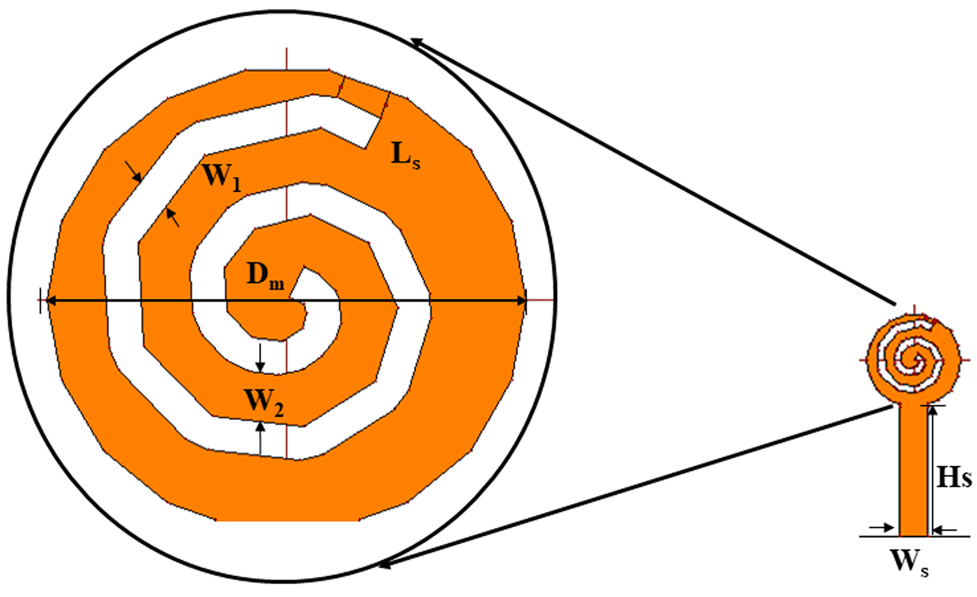
At the end the proposed structure (Antenna 4) is drafted by embedding an open-ended rectangular slot in the ground plane to filter Wi-MAX (3.5 GHz) and higher satellite X-band (8.5 GHz). The top and bottom view of Antenna 4 is demonstrated in Figs 1(e) and 1(f) respectively. Figure 2 illustrates the Archimedean spiral slot where W 1 denotes the width of the spiral slot, W 2 is the width of spiral ring, Dm being the diameter of the circular slot line transition and Ls being the total length of the spiral slot.
Demonstration of the spiral slot.

The spiral-shaped slot acts as a resonator which restrict the energy around the 5.20 GHz frequency level and as a result great attenuation near the notched frequency is observed. The first notch around 3.50 GHz is created by the open-ended slot inside the ground. In addition to this a third notch ranging from 8.50 to 9.30 GHz is achieved due to the spiral slot. Table 1 includes different parameters of the antenna alongside with dimensions.
Antenna parameters and dimensions

The first notch frequency (fnotch1) at around 3.95 GHz is produced because of the rectangular ground slot, where the notch frequency can be derived from the following equation:


where, fnotch1 = mid-frequency for first notch, c = velocity of light, LD = length of the DGS cut on the ground plane, WD = width of the DGS, and ɛreff = effective di-electric constant of the substrate.
Let P is considered to be the perimeter of the DGS and is given as P = 2(LD + WD) = 19.0 mm.
Now, P is taken in terms of free space wavelength as calculated by the equation:

where λ 0 is the free space wavelength corresponding to 3.95 GHz.
The second notch obtained has a range between 4.82 and 5.31 GHz following a bandwidth of 420 MHz centered precisely at 5.065 GHz. The second notch frequency (fnotch2) from Archimedean spiral of diameter Dm = 4.70 mm, length Ls = 14.2 mm and width of the slot W 1 = 0.50 mm is achieved from the following equation:

where, fnotch2 = second notch central frequency, Ls = length of spiral – shaped slot, W 1 = width of the spiral slot, Dm = diameter of the circular spiral structure.
The length of the spiral slot is also selected here as equal to the quarter wavelength and is given as

where λ 0 corresponds to free space wavelength for frequency at 5.20 GHz.
The third notch (fnotch3) centered around 8.90 GHz (8.50–9.30 GHz) is attained from diameter (Dm = 4.70 mm) of the circular spiral and the height (Hs = 6.825 mm) and width (Ws = 1.45 mm) of the strip connecting the Archimedean spiral slot from equation below

where fnotch3 = mid-frequency of third notch, Hs = height of the strip connecting spiral structure, Ws = width of the strip connecting spiral structure, Dm = diameter of the circular spiral.
Results and analysis
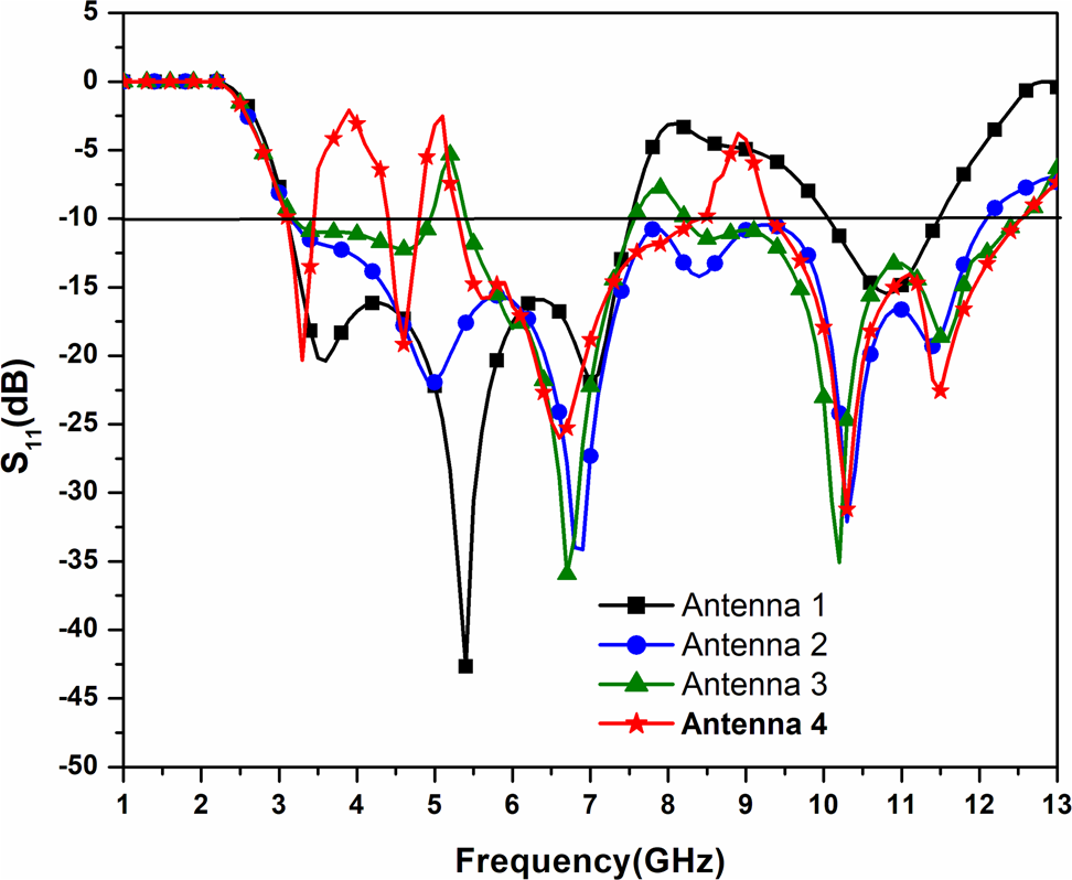
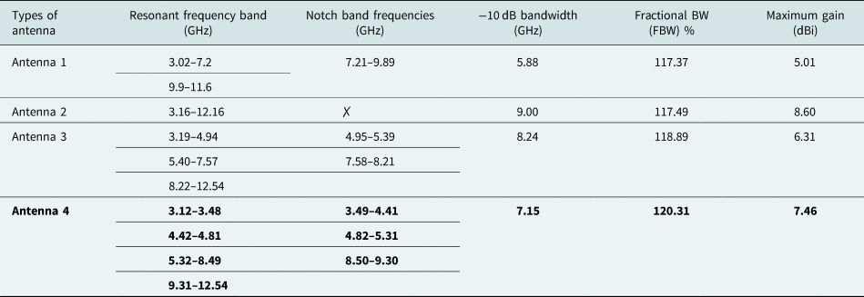
Figure 3 represents the variation of S 11 of the suggested antenna with reference to the other antennas. Antenna 1 shows wideband performance ranging from 3.02 to 7.20 GHz (4.18 GHz) and from 9.90 to 11.60 GHz (1.7 GHz). Antenna 2 exhibits UWB response with −10 dB impedance bandwidth extending from 3.16 to 12.16 GHz (9.0 GHz) covering both WLAN (2.4/3.2/5.2 GHz) and Wi-MAX (3.5/5.5 GHz) bands. Now to achieve notch characteristics further a spiral slot is embedded in a rectangular strip and denoted as Antenna 3.
S-Parameters versus frequency curve for all the antennas.

In Antenna 3, bandwidth ranges from 3.19 to 12.54 GHz producing a fractional bandwidth (FBW) of 118.89% with a notch band centered at around 5.20 GHz which filters WLAN (5.2 GHz) band and another band ranging from 7.58 to 8.21 GHz. Antenna 4 consists of triple notch bands ranging from 3.49 to 4.41 GHz, 4.82 to 5.31 GHz and from 8.50 to 9.30 GHz. Antenna 4 effectively suppress radiation characteristics around WLAN (5.2 GHz), Wi-MAX (3.50 GHz) bands, higher satellite X-band (8.50 GHz) and Aeronautical mobile band in India (8.965–9.040 GHz). The analysis of antenna types is shown in Table 2.
Performance analysis of different parameters of antenna 1, 2, 3 and 4

Note: FBW is computed abandoning notched bands allowing that S 11 ≤ 10 dB.
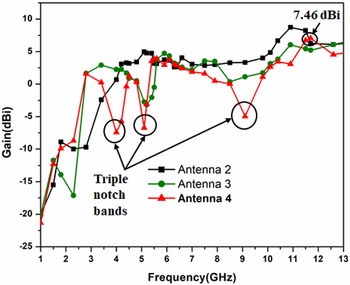
The difference in gain with respect to frequency for Antenna 4 is exhibited in Fig. 4, which points that there is a maximum peak gain of about 7.46 dBi at 11.30 GHz and the three notched region are clearly visible around 3.50, 5.20 and 8.50 GHz where the gain is minimum. The difference of Antenna 3 and 4 is in the imperfection of the ground plane in terms of a rectangular open slit which adds to the production of additional notch at 3.50 GHz and the position of the third notch band centered around 7.89 GHz in case of Antenna 3 to 8.90 GHz as in Antenna 4. A significant enhancement of maximum peak gain of the final antenna by about 1.15 dBi is achieved.
Comparison of gain for antenna 2, 3 and 4.

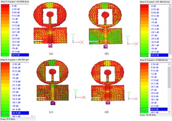
Surface current distribution around the spiral slot and the DGS is demonstrated in Figs 5(a) and 5(b) for two notch frequencies 3.50 and 5.20 GHz, respectively. The surface current is mostly centralized around the spiral slot thus changing current directions around the walls of the patch as shown in case of Figs 5(a) and 5(b) thus creating band stop effect in 3.50 and 5.20 GHz, respectively. It is seen that the surface current is mostly concentrated in the spiral slot and current direction alters with frequency change as found in passband frequencies of 5.50 and 10.25 GHz displayed in Figs 5(c) and 5(d), respectively.
Surface current distribution pattern at stop band frequencies of (a) 3.50 GHz and (b) 5.20 GHz and passband frequencies of (c) 5.50 GHz and (d) 10.25 GHz.

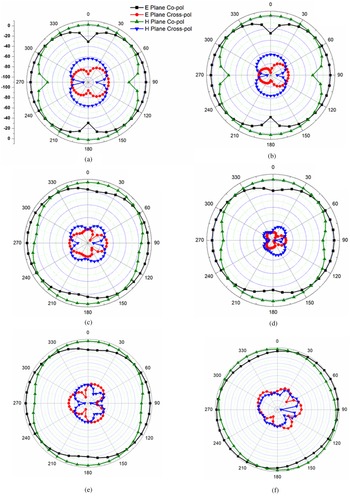
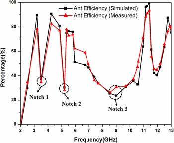
Figures 6(a), 6(d) and 6(f) represents Co pol and cross pol far-field patterns for X–Z and Y–Z directions for pass-band frequency of 3.20, 5.50 and 11.25 GHz while Fig. 6(b), 6(c) and 6(e) represent the far-field radiation patterns for the stop band frequency of 3.50, 5.20 and 9.00 GHz, respectively. It is seen from the figure that far-field patterns for H-plane is nearly omnidirectional throughout the UWB band. The E-plane pattern at lower frequencies are monopole like bidirectional in nature. As the frequency goes up that is at 11.25 GHz, tiny distortions are observed from Fig. 6(f) due to the increase of the electric length of the antenna at higher frequencies. The triple notch bands can be verified from the experimental and simulated antenna efficiency in Fig. 7. It is observed that the efficiency of the antenna reduces to 37.03% at 3.50 GHz, 30.31% at 5.20 GHz and 25.44% at 8.55 GHz while it is 89.65, 76.50, 75.92 and 99.30% at 3.20, 5.50, 5.80 and 11.40 GHz, respectively.
Measured far-field radiation patterns (Co-pol and cross pol) at (a) 3.20 GHz, (b) 3.50 GHz, (c) 5.20 GHz, (d) 5.50 GHz, (e) 9.0 GHz and (f) 11.25 GHz.

Simulated and measured antenna efficiency of antenna 4.

Parametric studies
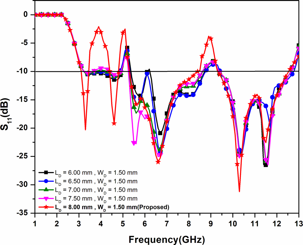
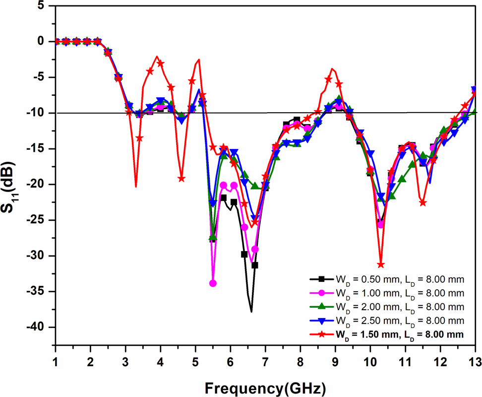
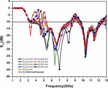
A parametric comparison is carried out for the proposed antenna. The simulations are carried out by varying the dimensions of the DGS of the antenna. The length of the rectangular ground slot (LD) is varied with width of the slot (WD) kept constant at 1.50 mm and changes in S-parameters are pointed out in Fig. 8. As seen clearly the proposed antenna has the best results for LD = 8.00 mm, while in other cases the notch bands are not prominent. Similar to the one above Fig. 9 shows the parametric study of variation of WD, keeping LD constant at 8.00 mm. When WD = 1.50 mm, the desired notch bands are achieved.
S-Parameter variation for values of LD (keeping WD constant at 1.50 mm).

S-Parameter comparison for separate values of WD (keeping LD constant at 8.00 mm).

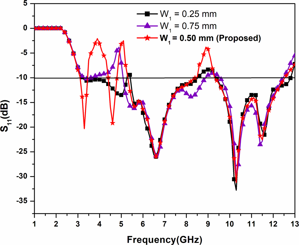
From equation (4), it is seen that W 1 is an important parameter in determining the stop band frequency of the second notch. So, a parametric analysis of W 1 is illustrated in Fig. 10 which indicates a significant change in the second notch frequency centered at 5.065 GHz by changing the value of W 1.
S-Parameter variation for different values of W 1.

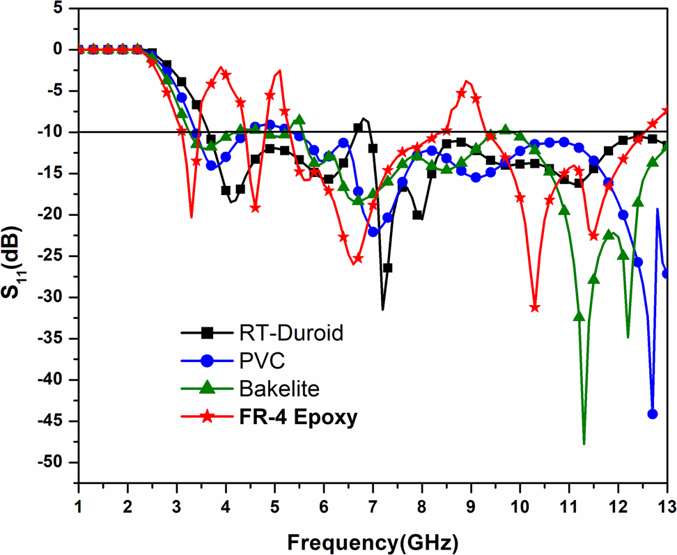
Substrates play a vital role in the geometry and performance of an antenna. The choice of substrate depends on cost-effectiveness and performance of the antenna on basis of gain, return loss and radiation pattern. From Fig. 11, it is seen that using FR-4 epoxy substrate (ɛ r = 4.40), the desired bands are filtered out. Fig. 12 denotes the changes in S-parameters while varying the length of the strip connecting the spiral slot (Hs). When Hs = 6.825 mm, the desired results are obtained keeping the other parameters of the spiral slot unchanged.
Comparison plot of S-parameters for antenna 4 using various substrates.

S-Parameter curve for different values of Hs.

Fabrication and measurement
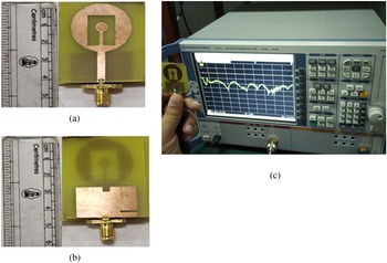
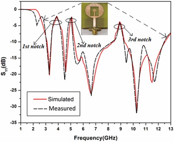
In this section, experiments are carried out to verify with the simulated results. The final fabricated antenna is shown in Figs 13(a) and 13(b). Rohde and Schwarz (ZVA-40) vector network analyzer was used to measure the radiation characteristics, the set-up of which is portrayed in Fig. 13(c) displaying the S-parameter response. Fig. 14 demonstrates both the simulated and experimental return loss characteristics.
(a) Top view of antenna 4, (b) bottom view of antenna 4, (c) VNA set up for measuring various antenna parameters.

S-Parameter analysis of antenna 4 (simulated versus measured).

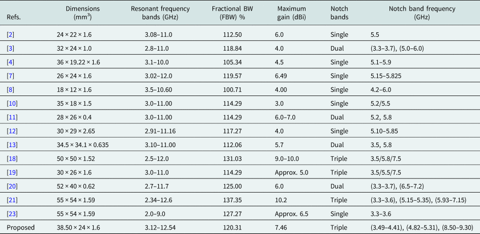
The experimental results are in good accordance with the simulated ones. The comparison of various radiation characteristics is portrayed in Table 3. Table 3 indicates the analysis of the suggested antenna accompanied by some reference antennas. It can be clearly pointed out from the table that although some antenna has some advantages in terms of dimensions as well as notch range but not as good as the other radiation characteristics in terms of radiation patterns, gain, antenna efficiency, etc.
Analogy of the final antenna (antenna 4) with previously proposed antennas.

Conclusions
In this research study, a compact circular UWB antenna is outlined which effectively filtrate WLAN (5.2 GHz), WiMAX (3.5 GHz) and higher satellite X bands (8.5 GHz). The installation of spiral slot in the patch produces notch band centered at 5.20 GHz, while open-ended rectangular slot in the ground plane produces notch centered at 3.95 GHz (3.49–4.41 GHz) and 8.90 GHz (8.50–9.30 GHz). Thus, the final proposed antenna produces triple notch bands attaining FBW of 120.31% ignoring the notch bands. In future this particular research effort can be carried out to the super wide band, where the operation can be extended in the range of 20 –30 GHz and also with the use of different substrates such as Teflon, Bakelite, PVC etc. The novel antenna not only acts as a filtenna to filter undesired interference from narrow bands such as WLAN (5.2 GHz) and WiMAX (3.5 GHz) but also gives added benefit in terms of triple notch characteristics by filtering higher satellite X band at 8.50 GHz.
 Arnab De received his B.Tech and M.Tech in Electronics and Communication Engineering from West Bengal University of Technology, West Bengal, India in the year of 2012 and 2014 respectively. He is currently a full-time Ph.D. research scholar at National Inst. of Technology, Durgapur, India. and a member of IEEE (Institute of Electrical and Electronics Engineers) and member of International Association of Engineers (IAENG). His current research areas includes the microstrip slotted antenna, defected ground structures, array antenna, etc. To his credit, he has many reputed international journals and conference publications in the fields of antenna engineering and wireless communications systems.
 Bappadittya Roy obtained B.Tech and M.Tech Degrees in Electronics and Communication Engineering from West Bengal University of Technology, West Bengal, India in 2008 and 2011 respectively. He obtained his Ph.D. degree in 2018 from the Department of Electronics and Communication Engineering at National Institute of Technology, Durgapur, West Bengal, India. Presently, he is attached to VIT-AP, University, Amaravati, India. He has several indexed publications including articles in reputed journals, conferences and book chapters. He is a senior member of IEEE (Institute of Electrical and Electronics Engineers). His research areas are microstrip antennas, fractal antennas and mobile communication. He has received many national and international travel grants and has travelled abroad for seminars, conferences and workshops
 Ankan Bhattacharya obtained B.Tech. and M.Tech. Degrees in Electronics & Communication Engineering from West Bengal University of Technology, Kolkata, India. He completed his Ph.D. from National Institute of Technology, Durgapur, India. He is the author of several research papers which have been published in many reputed journals and conferences of national and/or international levels. Dr Bhattacharya is a life-member of Forum of Scientists, Engineers & Technologists (FOSET), Member of Institution of Engineers India (IEI) and Member of International Association of Engineers (IAENG). His areas of research are antenna engineering, computational electromagnetics, electronic circuits and systems, signal processing, microwave devices and wireless communication technologies. He is also an editor/reviewer of many national/international journals of repute. He has organized/participated in, many national/international seminars, workshops and webinars. Presently he is associated with Mallabhum Institute of Technology, Bishnupur, India as an assistant professor of electronics & communication engineering department.
 Anup Kumar Bhattacharjee received his B.E. degree in Electronics and Telecommunication Engineering from B.E. College Shibpur, Howrah, India in 1983. He received M.E. and Ph.D. degrees from Jadavpur University, Kolkata, India in 1985 and 1989 respectively. Presently he is associated with National Institute of Technology, Durgapur, West Bengal, India as a senior professor of electronics and communication engineering department. His research areas are electronic devices and circuits, microwave devices, microstrip antennas, embedded systems, VLSI systems, mobile communications, satellite communications etc. Till date, he has successfully guided 25 Ph.D. students. He has more than 150 indexed publications to his credit. He has undertaken many significant academic and administrative responsibilities, throughout his vast 33 years of professional life.