I. INTRODUCTION
Bandpass filters (BPFs) are indispensable components in receiver front ends. Planar BPFs are preferred in wireless systems because they can be fabricated using printed circuit technology and are suitable for commercial applications due to their compact size and low cost of integration [Reference Hong and Lancaster1]. Over the years various techniques have been employed in design of multiband BPF. In [Reference Chang, Jang and Chen2], a compact dual-band BPF is presented by coupling hairpin shaped stepped impedance resonator (SIR) introduced by Makimoto and Yamashita [Reference Makimoto and Yamashita3]. Hairpin shaped half wavelength SIRs with interdigital coupling is used to design dual-band narrow BPF in [Reference Chu and Chen4]. The conventional half wavelength SIR underwent a transformation resulting in an asymmetric SIR. The direct implication was increased degree of design freedom as in addition to the impedance ratio, filter designers could also tune the electrical length ratio. This variant of SIR has been used to realize a fifth order dual-band BPF [Reference Jiang, Chang and Chin5]. Mutually exclusive dual passband has been reported in [Reference Kim and Chang6] where active devices like PIN diode have been incorporated with asymmetric SIR. Short ended SIRs have been utilized to design a dual mode dual-band BPF in [Reference Sun, Su, Kun, Wu and Chang- Hong7]. In [Reference Zhan and Zhu8], a set of four shorted λ/4 SIR have been used to implement a dual-band BPF with equal number of reflection and transmission zeros. Two different SIR dimensions have been coupled using interdigital capacitor to obtain dual passband BPF with a stopband till 7 GHz [Reference Sarkar, Ghatak, Pal and Poddar9]. Variable width coupled line segments and stepped impedance stubs are used to realize a dual passband BPF [Reference Wu, Zhou, Zhang, Liao and Liu10].
In this work investigations on a novel resonator configuration comprising of an asymmetric stepped impedance stub loaded uniform impedance open loop resonator (OLR) is presented. Precisely, a pair of inward folded half wavelength OLRs with asymmetric stepped impedance stub is utilized to generate two passbands at 2.45 and 3.5 GHz, respectively. In addition, three transmission zeros are obtained close to the passband that brings about high selectivity. An inherent wide stopband performance is achieved till 10 GHz. Rest of the paper is organized as follows. Section II deals with proposed asymmetric SIR type stub loaded OLR. Filter topology and analysis is discussed in Section III. Concluding remarks are given in Section IV.
II. ASYMMETRIC SIR SHAPED STUB LOADED OLR
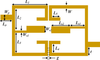
An inward folded OLR loaded with asymmetric SIR as a stub can be observed in the overall filter design as shown in Fig. 1. The substrate chosen for the design is RT Duriod 5880 which has relative dielectric constant 2.2 and height 0.787 mm. The outer OLR is designed to be half wave length long at 2.45 GHz. The impedance ratio of the asymmetric SIR is controlled to obtain the second passband at 3.5 GHz. This stub consists of narrow (high impedance) and wide sections (low impedance) with characteristic impedances Z s1, Z s2, respectively, and corresponding electrical lengths θ s1 and θ s2 which in turn are connected to an OLR. The impedance ratio K and the length ratio U of an asymmetric SIR are defined as follows.
 $$K = \displaystyle{{Z_{s2}} \over {Z_{s1}}}, $$
 $$U = \displaystyle{{\theta _{s2}} \over {\theta _{s1} + \theta _{s2}}}. $$
Layout of the proposed BPF. L 1 = 9.39, L 2 = 7.22, L 3 = 6.54, L 4 = 3.87, L 5 = 1.575, Ls 1 = 3.82, L s2 = 5.1, W = 0.88, W s1 = 0.37, W s2 = 1.85, g = 0.25, t = 3.1, and tap portion L p = 3.21, W p = 1.67 (all dimensions are in mm)

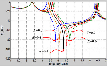
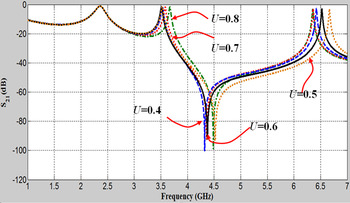
A conventional SIR [Reference Makimoto and Yamashita3] would have provided only one degree of freedom which is the impedance ratio. The use of asymmetric SIR enhances this design freedom by including the length ratio. Parametric study of the asymmetric stepped impedance stub loaded OLR is performed by loosely coupling the resonator to input/output (I/O) 50 Ω port. The resonance modes are identified and the effects of different design parameters on these modes are studied using transmission line model of the proposed resonator. From the parametric study of impedance ratio, a coarse value of K = 0.5 is found to be suitable to achieve the passband close to 3.5 GHz as indicated in Fig. 2. However, to bring the first spurious frequency at 3.5 GHz the value of K is fine tuned to 0.46. The parametric study of an asymmetric SIR shaped stub for various electrical length ratio U is shown in Fig. 3. The stub is designed with a find tuned value of U = 0.57 which is close to the desired frequency of 3.5 GHz. Eventually, it is seen that an asymmetric SIR shaped stub has provided increased degree of design freedom by which two parameters namely K and U can be fine tuned to obtain second mode at 3.5 GHz. It is observed, from parametric study of impedance ratio K and electrical length ratio U of asymmetric SIR, that second passband varies widely for change in K in comparison with that for the variation in U.
Parametric study of impedance ratio K of asymmetric SIR stub. A coarse value of U is taken as 0.6 for this study.

Parametric study of electrical length ratio U of asymmetric SIR stub. A coarse value of K is taken as 0.5 for this study.

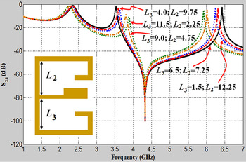
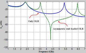
Next important design parameter is position of the asymmetric stub which is connected to a folded OLR. For this the length L 2 and L 3 decide the vertical position of the stub. The parametric study is shown in Fig. 4. One can observe that the parameters not only influence the second resonance but also the unwanted third spurious resonance also drastically varies. To achieve the desired passband frequency as well as to ensure that separation between second and third resonance is maximum, the position of the stub corresponding to L 2 = 7.25 and L 3 = 6.5 mm is obtained as indicated in Fig. 4. The values of L 2 and L 3 are fine tuned to 7.22 and 6.54 mm, respectively. Comparison of resonance characteristics of only OLR and asymmetric stepped impedance stub loaded OLR is as shown in Fig. 5. It can be observed that apart from introducing the second passband, the selectivity of this band is also improved by the introduction of a transmission zero at 4.3 GHz. As seen from the parametric study that the positions of transmission zero is also dependent on the asymmetric SIR design parameters. The ease in controlling the position of the transmission zero, second passband, as well control over position of third spurious resonance is brought about by the introduction of asymmetric stepped impedance as a stub. This enhances degree of design freedom with additional benefit of achieving wide upper stopband.
Parametric study of the stub position depending on variation of L 2 and L 3 for K = 0.46 and U = 0.57.

Resonance modes of only OLR and OLR loaded with asymmetric SIR as stub. For the asymmetric SIR shaped stub loaded OLR, the values of K = 0.46, U = 0.57, L 2 = 7.22, and L 3 = 6.54 mm.

III. FILTER DESIGN AND ANALYSIS
The filter design begins with the design of fundamental ingredient which is a resonator. The resonator is an asymmetric SIR stub loaded OLR that helps in achieving the resonance characteristics. The next step is to ensure proper coupling between the resonators to ensure passband bandwidth that includes all the channels of the desired bands. The final stage of design is to ensure proper extraction of the resonance modes with I/O feed lines. The I/O coupling is realized by a 50 Ω tap line as shown in layout of the dual-band BPF given in Fig. 1. The tap position “t” and separation “g” between the outer resonators as indicated in Fig. 1 are optimized to achieve the passband bandwidth that includes all channels in these bands. A tap position of 3.1 mm and spacing 0.25 mm between the outer resonators is found to be suitable for achieving passband bandwidth that covers the desired frequency bands.
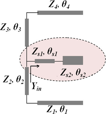
The transmission line model of this dual-band resonator is shown in Fig. 6. The outer resonator impedances are same because it is a uniform impedance resonator. To analyze the net equivalent transmission line model of the proposed filter, total ABCD matrix is obtained from the transmission line model of proposed resonator as illustrated in Fig. 6. The ABCD matrix of a transmission line is given by
 $$\left[ {\matrix{ A & B \cr C & D \cr}} \right] = \left[ {\matrix{ {\cos \theta} & {jZ_0 \sin \theta} \cr {jY_0 \sin \theta} & {\cos \theta} \cr}} \right],$$
where θ indicates the electrical lengths θ 1, θ 2, θ 3 or θ 4 which are computed for this design as θ 1 = θ 4 = 57.79°, θ 2 = 23.98°, and θ 3 = 27.60° computed at 2.45 GHz and correspondingly Z 0 indicates impedances Z 1, Z 2, Z 3, and Z 4 for the various segments of the uniform impedance resonators with reference to Fig. 6. The overall matrix for the resonator is a product of five ABCD matrices which includes a matrix for the asymmetric stub portion. The net ABCD matrix of this resonator is given below
 $$\eqalign{\left[ {\matrix{ {A_T} & {B_T} \cr {C_T} & {D_T} \cr}} \right] & = \left[ {\matrix{ {A_1} & {B_1} \cr {C_1} & {D_1} \cr}} \right] \times \left[ {\matrix{ {A_2} & {B_2} \cr {C_2} & {D_2} \cr}} \right] \times \left[ {\matrix{ {A_s} & {B_s} \cr {C_s} & {D_s} \cr}} \right] \cr & \times \left[ {\matrix{ {A_3} & {B_3} \cr {C_3} & {D_3} \cr}} \right] \times \left[ {\matrix{ {A_4} & {B_4} \cr {C_4} & {D_4} \cr}} \right],}$$
 $$\left[ {\matrix{ {A_s} & {B_s} \cr {C_s} & {D_s} \cr}} \right] = \left[ {\matrix{ 1 & 0 \cr {Y_{in}} & 1 \cr}} \right],$$
where
 $$Y_{in} = - jY_{s1} \displaystyle{{Z_{s1} \tan \theta _{s2} + Z_{s2} \tan \theta _{s1}} \over {Z_{s1} \tan \theta _{s1} \tan \theta _{s2} - Z_{s2}}}. $$
Transmission line model of the proposed asymmetric stepped impedance stub loaded OLR.

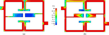
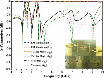
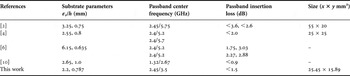
The overall ABCD matrix of the equivalent transmission model including the I/O as well as inter resonator coupling of proposed dual-band BPF is computed using an in house developed MATLAB™ code to obtain the |S 11| (dB) and |S 21| (dB). The proposed filter is also simulated using electromagnetic (EM) simulator CST Microwave Studio™. Current distribution as shown in Fig. 7 is obtained from EM simulation confirming the design that establishes the fact that outer resonator contributes to 2.45 GHz and asymmetric SIR based stub is effective in tuning the second passband at 3.5 GHz. The stubs do not support any current flow at the first band. However, current flow in the stubs establishes its contribution to the second resonance. A fabricated prototype is developed as shown in inset of Fig. 8 that shows the S-parameter. The measured S-parameters using Rohde & Schwarz ZVA 40 VNA are in close agreement to that obtained by EM simulation as well as that from transmission line model. The measured insertion loss of the two passbands is within 1.5 dB. The measured 10 dB passband bandwidth at first as well as second band is 250 MHz. This results in a 10.2 and 7.2% fractional bandwidth at the first and second passband, respectively. Three transmission zeros as obtained from measurement are at 2.1, 3.05, and 3.95 GHz, respectively, that improves the selectivity of the desired passbands. The first two are due to source load coupling and the third one due to the asymmetric SIR stub is explained in Section II. However, the net coupling effect results in a shift from 4.3 to 3.95 GHz. An upper stopband till 10 GHz is obtained with measured attenuation better than 10 dB. The overall dimension of the designed dual-band BPF including the I/O fed lines is 25.45 × 15.89 mm2. A comparison of the proposed work with other related works is given in Table 1.
Current distribution at (a) 2.45 GHz, and (b) 3.5 GHz.

Comparison between s-parameter obtained from full wave EM simulation, transmission line model and measurement.

Comparison with other related dual band BPFs.

IV. CONCLUSION
A compact dual-band BPF filter is presented by using a novel resonator configuration realized by loading an inward folded OLR with asymmetric stepped impedance open stub resonator that creates two passbands at 2.45 and 3.5 GHz, respectively. It is seen that the asymmetric stub provides increased degree of design freedom in tuning the passband, positioning the transmission zero as well as shifting the third spurious band away from the second passband. A wide upper stopband is realized till 10 GHz. The overall dimension of the proposed filter is 25.45 × 15.89 mm2 which renders the compact size.
 Manimala Pal received her M. Tech. (Microwave Engineering) from The University of Burdwan in 2010. She started her research in microwave circuits at Radionics Laboratory with Dr. Rowdra Ghatak. Presently she holds a faculty position in Electronics and Communication Engineering Department of NSHM Knowledge campus, Durgapur Group of Institutions, Durgapur, West Bengal. She set up the Radio Engineering and Antenna Laboratory with the introduction of openwares in electromagnetic simulation at her Institute from where many undergraduate students have done commendable work. Her areas of interest lie in design and optimization of planar bandpass filters, fractal shaped antennas for multiband and UWB communication, metamaterials, RFID, computational electromagnetics and planar couplers. She has more than 50 publications in various international and national journal as well as conferences. She is a regular reviewer of IEEE (USA), IET (UK), and Progress in Electromagnetics Research journals. She is a member of microwave and antenna research group at NIT Durgapur as an external fellow. She has been convener and technical program chair in IEEE workshops in microwave engineering.
 Rowdra Ghatak received his M. Tech. (Microwave Engineering) from The University of Burdwan and Ph.D. (Engg) from Jadavpur University in 2002 and 2008, respectively. Presently he is a professor in Electronics and Communication Engineering department of National Institute of Technology Durgapur. He is a recipient of the URSI Young Scientist Award in 2005. He has recently received support under DST Young Scientist scheme for development of UWB antennas for imaging RADAR. He has more than 180 publications in various National/International journals and conferences. His research interest lies in the areas of fractal antenna, metamaterial, application of evolutionary algorithms to electromagnetic optimization problems, RFID, computational electromagnetic and microwave passive circuit design. He is a reviewer of IEEE, IET, Elsevier, JEMWA, Journal from Brazilian Microwave Association, John Wiley and PIER journals. He is a member of IEEE and has organized workshops in the capacity of workshop chair/convener on Microwave Circuits and Antenna.
 Pankaj Sarkar received his M. Tech. degree from University of Burdwan University in 2009. He worked 1 year in Space Applications Center – Ahmedabad as a trainee for M. Tech. project entitled as “Design of MMIC Mixer at 50–60 GHz”. He initiated his teaching career from ITER (Siksha “O” Anusandhan University-Bhubaneswar), after that he served Sikkim Manipal Institute of Technology and National Institute of Technology-Sikkim. Presently he is Assistant Professor in Electronics and Communication Engineering Department of North-Eastern Hill University-Shillong. He has more than 30 publications in various National/International journals and conferences. His research interest lies in the area of microwave passive circuit design, metamaterials, MMIC, antenna. Presently he is pursuing Ph.D. from Jadavpur University. He is a reviewer of many international and national journals.