I. INTRODUCTION
Monocrystalline silicon is a fundamental material for making semiconductor devices and micro/nano-electro-mechanical systems.Reference Petersen1,Reference Blanco, Chomski, Grabtchak, Ibisate, John and Leonard2 An in-depth understanding of the deformation mechanisms of silicon can provide remarkably useful information for improving the mechanical, optical, and electrical performance of the related products. Indentation techniques, in particular, nanoindentation, have been widely used to probe mechanical properties of silicon, e.g., hardness and Young’s modulus, and to understand the phase transformation events, a major mechanism of plasticity in silicon caused by mechanical loading.Reference Gerk and Tabor3–Reference Fang, Chang and Lin10
Monocrystalline silicon is brittle under simple tension at ambient temperature but exhibits significant plasticity via complicated phase transformations when subjected to complex loading with sufficient hydrostatic and shear stresses.Reference Zhang and Zarudi11 A full understanding of phase transformation and defect nucleation in subsurface in silicon under nanoindentation can provide valuable information for measuring mechanical characteristics and optimizing the machining conditions to achieve high surface finish with damage-free subsurface. In the last several decades, the phase transformations in monocrystalline silicon induced by micro/nanoindentation have been extensively studied both experimentally and theoretically.Reference Pharr, Oliver and Harding5,Reference Weppelmann, Field and Swain7,Reference Kailer, Gogotsi and Nickel12–Reference Chang and Zhang19 For example, a detailed molecular dynamics analysis of nanoindentation of silicon monocryatals showed that the inelastic deformation of silicon is solely caused by amorphous phase transformation and the onset of such inelastic deformation can be well predicted by a stress criterion.Reference Zhang and Tanaka14,Reference Zhang and Tanaka15 Gerbig et al.Reference Gerbig, Michaels, Forster and Cook18 studied the indentation-induced phase transformation processes by in situ Raman microspectroscopy of the deformed contact region of silicon on sapphire samples during contact loading and unloading. The indenter was a conospherical diamond tip with a tip curvature of 50 μm. The reported in situ experiments provide insights on the transformation processes in Si during indentation. The nanoindentation tests under an ultra-low range of loads with various loading rates using a Berkovich indenter (Hysitron, Eden Prairie, MN) with a tip radius of 227 nm were investigated by Chang and Zhang.Reference Chang and Zhang19 It was found that with a proper area function of the indenter tip, the mechanical properties of silicon can be accurately characterized, that a pop-in event may occur upon ultra-low loading and represents the onset of phase transition, and that a lower loading rate favors a sudden volume change. Specially, a damage-free and chemical-free silicon polishing technique has recently been developed based on the stress-controlled phase transformation mechanisms.Reference Zhang, Biddut and Ali20,Reference Biddut, Zhang, Ali and Liu21
At the same time, some authors reported experimentally the deformation-induced microdefects, such as stacking faults, dislocations and cracks in silicon under indentation with large loads and a large radius tip.Reference Zarudi and Zhang13,Reference Bradby, Williams, Wong-Leung, Swain and Munroe22–Reference Jang and Pharr29 For example, Zarudi and ZhangReference Zarudi and Zhang13 analyzed the subsurface structure of indented mono-crystalline silicon by means of high-resolution electron microscopy on cross-section view samples. To understand the micro-structural changes with respect to indentation, a series of tests were conducted under total indentation loads of 30, 40, 50, 70, 90, and 100 mN, respectively. It was found that there are always some planar defects emanating from the bottom of the transformation zone under a small indentation load. Some microcracks emerge at the defects intersection when the indentation load increases. Some transmission electron microscopy observations of the deformation microstructure under spherical and Berkovich indentations in silicon were studied by Bradby et al.Reference Bradby, Williams, Wong-Leung, Swain and Munroe22,Reference Bradby, Williams, Wong-Leung, Swain and Munroe23 with slip bands visible in the cross-sectional transmission electron microscopy (XTEM) micrographs. Lloyd et al.Reference Lloyd, Molina-Aldareguia and Clegg24,Reference Lloyd, Castellero, Giuliani, Long, McLaughlin, Molina-Aldareguia, Stelmashenko, Vandeperre and Clegg25 examined deformation under nanoindents in undoped semiconductor single crystals Si through transmission electron microscope (TEM). The dislocation generation and crack were observed around the transformed zone. Zarudi et al.Reference Zarudi, Zhang, Cheong and Yu26 analyzed the microstructure of monocrystalline silicon after indentation with a Berkovich indenter. Cross-sectional view TEM samples were used to explore the detailed distributions of various microstructures in the subsurface of indented silicon. It was found that microcracks were always generated at the bottom of the deformation zone under total indentation loads of 20, 50, and 90 mN, respectively. A modified plastic damage model that accounts for tensile damage and compressive plasticity as well as interactions among them was adopted to simulate the indentation induced cracking of silicon under Berkovich, cube corner, and Vickers indenters by Wan et al.Reference Wan, Shen, Chen and Chen27 JianReference Jian28 investigated the contact-induced structural deformation behaviors in single-crystal Si(100) and MOCVD-deposited GaN thin films by using a combination of nanoindentation, micro-Raman spectroscopy, FIB, and TEM techniques. The micro-Raman analysis, measured from the indented materials which had plastically deformed on loading, showing a phase transformation occurs in Si, whereas the results for GaN thin films do not give sufficient evidence for phase transformations. The influence of indenter angle on the nanoindentation cracking behavior of single crystal Si and Ge was systematically explored by Jang and PharrReference Jang and Pharr29 through nanoindentation experiments with a series of triangular pyramidal indenters with different centerline-to-face angles. The relationships between indentation load, crack length and indentation size and their dependence on indenter angle were carefully examined and compared with previous indentation cracking studies.
The nucleation and emission of dislocations under nanoindentation is an active area of both experimental and theoretical studies.Reference Gerberich, Nelson, Lilleodden, Anderson and Wyrobek30–Reference Minor, Syed Asif, Shan, Stach, Cyrankowski, Wyrobek and Warren37 With substantial guidance from experimental results and atomistic simulations, the onset of plasticity during nanoindentation is now widely believed to be associated with homogeneous dislocation nucleation for many kinds of materials.Reference Tadmor, Miller, Phillips and Ortiz31–Reference Minor, Syed Asif, Shan, Stach, Cyrankowski, Wyrobek and Warren37 However, for monocrystalline silicon under indentation, both experimentalReference Chang and Zhang19 and theoreticalReference Zhang and Tanaka14,Reference Zhang and Tanaka15,Reference Zhang, Biddut and Ali20,Reference Biddut, Zhang, Ali and Liu21 studies have shown that under a high hydrostatic pressure, the first phase transformation to take place in silicon will be from the semiconducting silicon (Si-I) to the metallic state (Si-II). Then, as the shear stress on some slip planes caused by nanoindentation reaches the critical shear stress for nucleating dislocations, the dislocation will appear or emit.Reference Lorenz, Zeckzer, Hilpert, Grau, Johansen and Leipner38–Reference Wu, Huang, Zou, Zhang and Dell41 To date, however, no analytical model is available to predict the threshold stress and state of stress of the dislocation initiation in silicon under nanoindentation,Reference Lorenz, Zeckzer, Hilpert, Grau, Johansen and Leipner38–Reference Wasmer, Gassilloud, Michler and Ballif42 although a quantitative evaluation of the critical load is vital to the development of damage-free machining of silicon for semiconductor industry.
On the other hand, Minor et al.Reference Minor, Lilleodden, Jin, Stach, Chrzan and Morris43 presented direct observations of room temperature dislocation plasticity in single crystalline silicon at room temperature during indentation. In contrast to the observations of phase transformation during most conventional indentation experiments, the unique geometry used for the in situ experiments resulted in dislocation plasticity and no phase transformation. The results of finite-element modeling suggested that the presence of free surfaces in unique sample geometry leads to preferential surface nucleation of dislocations and the suppression of phase transformation. At the same time, the research of Ge et al.Reference Ge, Minor, Stach and Morris44 demonstrated as the sample thickness decreases to the indentation size, dislocation plasticity becomes more important. At sufficiently small sample width, phase transformations disappear and dislocation plasticity is the mechanism of deformation. The change in mechanism was due to the relative ease of nucleating dislocations in the thin sample, which is believed to be a consequence of the change in the indentation stress field. We think the change in mechanism of deformation is very important to investigate the subsurface damage and material removal mechanism in nanoscale manufacture of silicon. Deneen et al.Reference Deneen, Mook, Minor, Gerberich and Carter45 investigated the mechanical behavior of silicon nanospheres in the TEM using an in situ indentation sample holder. In the silicon particles, both elastic and plastic deformation has been observed, and the exact moment of nanoparticle fracture has been illustrated. The deformation of single-crystal Si nanospheres and submicron pillars had been measured experimentally in compression by Stauffer et al.,Reference Stauffer, Beaber, Wagner, Ugurlu, Nowak, Mkhoyan, Girshick and Gerberich46 Stauffer,Reference Stauffer47 and Gerberich et al.Reference Gerberich, Stauffer, Beaber and Tymiak48 The results indicated dislocations can be nucleated in nanoparticles and submicron pillars under compressive stresses without a phase transformation. Garcia-ManyesReference Garcia-Manyes, Güell, Gorostiza and Sanz49 had experimentally demonstrated that the yield threshold value occurs at a force lower than that ever reported experimentally. The elastic region of the surface does not follow the Hertz equation but, instead, can be fitted to their proposed spring model. Furthermore, they differentiated between differently oriented silicon surfaces, thus highlighting the importance of anisotropy on the mechanical response of the system even at the nanometer scale. The above investigationsReference Minor, Lilleodden, Jin, Stach, Chrzan and Morris43–Reference Garcia-Manyes, Güell, Gorostiza and Sanz49 indicate that dislocation plasticity is dominant in in situ experiments while absent in conventional nanoindentation tests, lies in the change of sample geometry and stress state of the indentation. Conventional indentation experiments are done on bulk samples that are, in effect, flat half-spaces (e.g., a silicon wafer). The load produced by indentation into a half-space is well described by the Hertzian stress field, in which the maximum shear stress is developed beneath the surface.Reference Minor, Lilleodden, Jin, Stach, Chrzan and Morris43
The objective of this study is to establish an analytical model that will be capable of taking into account the phase transformation in determining the critical load of the generation and emission of partial dislocations in silicon wafer under indentation. In the modeling, we will follow the deformation process already explored by experiment and molecular dynamics that phase transformation first takes place under indentation, followed by partial dislocations emitting from the interface between the transformed zone and the originally crystalline silicon when the indentation load reaches to a critical value. The critical indentation pressure for the emission of the partial dislocation will be determined and the effects of the indenter geometry and the location of dislocation nucleation will be analyzed.
II. MODEL DESCRIPTION
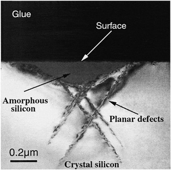
To establish the theoretical model to study the dislocation nucleation and emission under nanoindentation in silicon, let us briefly describe first the experimental results of subsurface deformation based on the work by Zarudi and Zhang.Reference Zarudi and Zhang13 Their indentation experiments were conducted on precisely polished (100) surfaces of mono-crystalline silicon with rms surface roughness less than 2 nm. The indentation with a spherically tipped diamond indenter of radius 5 μm was made on a UMIS-2000 instrument (CSIRO, Australia). The mechanically deformed regions were examined by means of a TEM. These samples were then cleaved along the (011) planes with their surface normal close to the [011] direction. The subsurface structure of silicon at an indentation load of 40 mN is shown in Fig. 1, which shows that the transformation zone is located in the immediate vicinity of the subsurface region and has nearly a hemispherical shape. There are some defects emanating from the bottom of the transformation zone lying in the {111} planes. Using the selected area electron diffraction pattern, Zarudi and ZhangReference Zarudi and Zhang13 had shown that these defects were planar defects, such as stacking faults.
Subsurface deformation at the indentation load of 40 mN (Ref. Reference Zarudi and Zhang13).

The above resultsReference Zarudi and Zhang13 and many other indentation testsReference Bradby, Williams, Wong-Leung, Swain and Munroe22–Reference Jang and Pharr29 demonstrate that the subsurface residual deformation induced by indentation are phase transformations and defect. Zhang and Zarudi,Reference Zhang and Zarudi11 Zhang and Tanaka,Reference Zhang and Tanaka14,Reference Zhang and Tanaka15 Biddut et al.,Reference Zhang, Biddut and Ali20,Reference Biddut, Zhang, Ali and Liu21 Lorenz et al.,Reference Lorenz, Zeckzer, Hilpert, Grau, Johansen and Leipner38 Gassilloud et al.,Reference Gassilloud, Ballif, Gasser, Buerki and Michler39 and Wu et al.Reference Wu, Huang, Zou and Dell40,Reference Wu, Huang, Zou, Zhang and Dell41 demonstrated that phase transformation always takes place before the emerge of dislocations and planar defects during nanoindentation and nanoscratching in silicon.
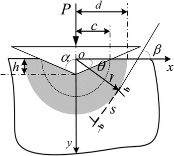
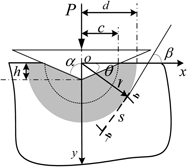
Based on the experimental results availableReference Zarudi and Zhang13,Reference Bradby, Williams, Wong-Leung, Swain and Munroe22,Reference Bradby, Williams, Wong-Leung, Swain and Munroe23,Reference Zarudi, Zhang, Cheong and Yu26,Reference Lorenz, Zeckzer, Hilpert, Grau, Johansen and Leipner38–Reference Wasmer, Gassilloud, Michler and Ballif42 and the above analysis, we can establish the following theoretical model to explore the critical indentation load for the emission of partial dislocations during nanoindentation. The model is illustrated in Fig. 2, where the indentation is made on the (100) surface under an indentation load P. The conical indenter with a relatively large radius tip and a semi angle α is considered to be rigid. The indentation depth and the radius of contact circle between the indenter and the silicon material are h and c, respectively. Since the phase transformation has taken place before defect emission and the phase transformation zone is nearly hemispherical with radius r = d under relatively small loads, it is reasonable to anticipate that the emission of a partial lattice dislocation emits from the boundary of the phase transformed zone into the bulk of silicon when the indentation load increases to a critical value under the indention-induced shear stresses. More precisely, the emission process represents the generation of a dipole of Shockley partial dislocations with Burgers vectors  ${\bf{b}}$ and
 $- {\bf{b}}$, called b-dislocation and (−b)-dislocation, respectively.Reference Wasmer, Gassilloud, Michler and Ballif42,Reference Minor, Lilleodden, Jin, Stach, Chrzan and Morris43 The b-dislocation of the dipole under consideration here is immobile (it is located at the boundary of the phase transformed zone), whereas the (−b)-dislocation moves into the bulk of silicon (Fig. 2). The mobile partial (−b)-dislocation slips along a crystallographic plane that makes an angle β with the surface plane, and a stacking fault is formed in its wake. The stacking fault length s is equal to the distance moved by the (−b)-dislocation. According to the experimental observation, slip bands can be clearly seen in micrographs oriented at an angle of about 54° to the (100) surface, which indicates that they are along the {111} planes.Reference Zarudi and Zhang13,Reference Lloyd, Castellero, Giuliani, Long, McLaughlin, Molina-Aldareguia, Stelmashenko, Vandeperre and Clegg25,Reference Zarudi, Zhang, Cheong and Yu26 In the modeling, we take β = 54° and consider Shockley partial dislocations of the edge 90°-type. Each partial dislocation is specified by the Burgers vector b = a/
 $\sqrt 6$, where a is the lattice parameter.
Schematic description of the indentation-induced emission of a Shockley partial dislocation.

III. DISLOCATION EMISSION CRITERION
Let us examine the energy characteristics of the Shockley partial dislocation emission under nanoindentation. The emission process is specified by the energy change ΔW = W 2 − W 1, where W 1 is the energy of the initial state of the system before the dislocation emission, and W 2 is that after the emission. This process is energetically favorable if the energy change per unit dislocation length is negative.Reference Ovid’ko and Skiba50–Reference Hirth and Lothe52
 $$\Delta W = {W_2} - {W_1} \,\le \,0\quad ,$$
where ΔW can be expressed as
 $$\Delta W = {E^0} + {E^{\rm{\gamma }}} + {E^b} - {E^I}\quad ,$$
in which E 0 is the total energy of the dislocation cores, E γ is the band energy of the stacking fault, E b is the elastic energy of the partial dislocation dipole, and E I is the work of the external shear stress used to glide the (−b)-dislocation.
The energy components E 0 and E γ can be written asReference Ovid’ko and Skiba50–Reference Hirth and Lothe52
 $$E^0 = Gb^2 /[2{\rm{\pi }}(1 - {\rm{\nu }})]E^{\rm{\gamma }} = s{\rm{\gamma }}_{{\rm{st}}} \quad ,$$
where G is the shear modulus and ν is Poisson ratio of silicon, and γst denotes the stacking fault energy per unit area.
The elastic energy of the dislocation system E b, including the interaction of partial dislocations with the surface and that with one another, can be calculated using the relations for the stress fields of an edge dislocation located near a surface. Based on the theory of dislocations,Reference Hirth and Lothe52,Reference Freund and Suresh53 we find the following expression of E b
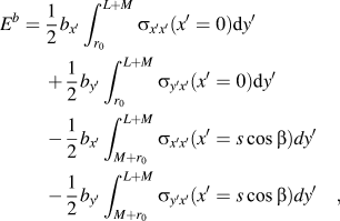 $$\eqalignb{ E^b = \,{1 \over 2}b_{x'} \int_{r_0 }^{L + M} {{\rm{\sigma }}_{x'x'} (x' = 0){\rm{d}}y'} \cr+ {1 \over 2}b_{y'} \int_{r_0 }^{L + M} {{\rm{\sigma }}_{y'x'} (x' = 0){\rm{d}}y'} \cr - {1 \over 2}b_{x'} \int_{M + r_0 }^{L + M} {{\rm{\sigma }}_{x'x'} (x' = s\cos {\rm{\beta }})dy'} \cr- {1 \over 2}b_{y'} \int_{M + r_0 }^{L + M} {{\rm{\sigma }}_{y'x'} (x' = s\cos {\rm{\beta }})dy'} \quad , \cr} $$
where  ${b_{x'}} = b\cos \beta$,
 ${b_{y'}} = b\sin \beta$, L = rsinθ, M = ssinβ, and r 0 is the dislocation core radius. By using the Airy stress function method,Reference Freund and Suresh53 stresses
 ${{\rm{\sigma }}_{x'x'}}$ and
 ${{\rm{\sigma }}_{y'x'}}$ can be determined as
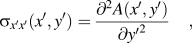 $${{\rm{\sigma }}_{x'x'}}(x',y') = {{{\partial ^2}A(x',y')} \over {\partial {{y'}^2}}}\quad ,$$
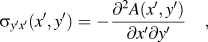 $${{\rm{\sigma }}_{y'x'}}(x',y') = - {{{\partial ^2}A(x',y')} \over {\partial x'\partial y'}}\quad ,$$
 $$\eqalignb{ A(x',y') = {G \over {2{\rm{\pi }}(1 - {\rm{\nu }})}}[ {{1 \over 2}(x'b_{y'} - y'b_{x'} )\ln ( {{{x'^2 + y'^2 } \over {x'^2 + (2L + 2M - y')^2 }}} ) + {{2b_{y'} x'(L + M - y') + b_{x'} (L + M)[x'^2 + 2y'(M + L) - y'^2 ]} \over {x'^2 + (2L + 2M - y')^2 }}} ] \cr- {G \over {2{\rm{\pi }}(1 - {\rm{\nu }})}}[ {{1 \over 2}(x'b_{y'} - y'b_{x'} )\ln ( {{{x'^2 + y'^2 } \over {x'^2 + (2L - y')^2 }}} ) + {{2b_{y'} x'(L - y') + b_{x'} (L)(x'^2 + 2y'L - y'^2 )} \over {x'^2 + (2L - y')^2 }}} ]\quad . \cr} $$
Substituting Eqs. (5)–(7) into Eq. (4), the elastic energy of partial dislocations, E b, can be obtained. The explicit expression of this elastic energy is very complicated. According to Freund and Suresh,Reference Freund and Suresh53 for most purposes, the logarithmic term in Eq. (7) is the dominant contribution to E b. Therefore, E b can be approximately simplified to
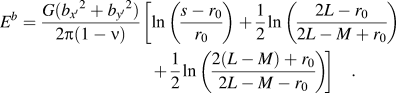 $$\!{E^b} =\,{{G({b_{x'}}^2 + {b_{y'}}^2)} \over {2{\rm{\pi }}(1 - {\rm{\nu }})}} [ {\ln ( {{{s - {r_0}} \over {{r_0}}}} ) + {1 \over 2}\ln ( {{{2L - {r_0}} \over {2L - M + {r_0}}}} ) + {1 \over 2}\ln ( {{{2(L - M) + {r_0}} \over {2L - M - {r_0}}}} )]\quad.$$
If the (−b)-dislocation is not considered, the expression of the energy can be further simplified from Eq. (4) to
 $${E^b} = {{G({b_{x'}}^2 + {b_{y'}}^2)} \over {4{\rm{\pi }}(1 - {\rm{\nu }})}}\ln \left( {{{2L - {r_0}} \over {{r_0}}}} \right)\quad ,$$
which is in agreement with the result of Freund and SureshReference Freund and Suresh53 when a dislocation is located near the surface (with a distance L from the surface).
The work of the external stresses caused by indentation E I is given byReference Hirth and Lothe52
 $$\eqalignb{ E^I = \,b_{x'} \int_{r\cos {\rm{\theta }} - s\cos {\rm{\beta }}}^{r\cos {\rm{\theta }}} {{\rm{\sigma }}_{xy} (y = r\sin {\rm{\theta }} + s\sin {\rm{\beta }}){\rm{d}}x} + b_{x'} \int_{r\sin {\rm{\theta }}}^{r\sin {\rm{\theta }} + s\sin {\rm{\beta }}} {{\rm{\sigma }}_{xx} (x = r\cos {\rm{\theta }}){\rm{d}}y} \cr+ b_{y'} \int_{r\cos {\rm{\theta }} - s\cos {\rm{\beta }}}^{r\cos {\rm{\theta }}} {{\rm{\sigma }}_{yy} (y = r\sin {\rm{\theta }} + s\sin {\rm{\beta }}){\rm{d}}x} \cr+ b_{y'} \int_{r\sin {\rm{\theta }}}^{r\sin {\rm{\theta }} + s\sin {\rm{\beta }}} {{\rm{\sigma }}_{xy} (x = r\cos {\rm{\theta }}){\rm{d}}y} \quad , \cr} $$
where σxx, σyy, and σxy are stress components in the elastic zone (i.e., in the zone that the silicon remains crystalline).
Here we assume that under a high pressure, the first phase transformation to take place in silicon will be from the semiconducting silicon (Si-I) to the metallic state (Si-II). We should realize that the two phases, Si-I and Si-II, have different crystal structures and different shear moduli. Some molecular dynamics studies also showed a large modulus change when the phase transformation occurred. Due to the complexity of stress fields, we only consider a single phase material as a simplified model in the current paper. According to Galanov et al.Reference Galanov, Domnich and Gogotsi54 and Vodenicharova and Zhang,Reference Vdenitcharova and Zhang55,Reference Vodenitcharova and Zhang56 phase transformation can be interpreted as the plastic deformation induced by nanoindentation. Therefore, the stress fields induced by the indentation accounting for the phase transformation can be calculated by means of the elastic–plastic contact mechanics. Hence, the stress fields σxx, σyy, and σxy can be constructed as the superposition of the elastic stresses induced by the purely elastic indentation and the residual stresses due to local plastic deformation surrounding the indenter. The purely elastic stresses are estimated by a Hertzian elastic field and the residual stresses can be estimated by a blister-field obtained by Yoffe.Reference Yoffe57 According to YoffeReference Yoffe57 and Feng et al.,Reference Feng, Qu, Huang and Nix58,Reference Feng, Qu, Huang and Nix59 stresses σxx, σyy, and σxy can be expressed as:
 $$\eqalign{ {\rm{\sigma }}_{xx} = {{3P} \over {2{\rm{\pi }}c^2 }}\{ {{{1 - 2{\rm{\nu }}} \over 3}{{c^2 } \over {x^2 }}[ {1 - ( {{y \over w}} )^{3} } ] + ( {{y \over w}} )^{3} {{c^2 w^2 } \over {w^4 + c^2 y^2 }} + {y \over w}[ {{{w^2 (1 - {\rm{\nu }})} \over {w^2 + c^2 }} + (1 + {\rm{\nu }}){w \over c}\tan ^{ - 1} ( {{c \over w}} ) - 2} ] \} \cr+ {{2B} \over {(x^2 + y^2 )^{{3 \over 2}} }}[ {{{x^2 y^2 (5 - 2{\rm{\nu }})} \over {(x^2 + y^2 )^2 }} - {{x^2 (4 - 2{\rm{\nu }})} \over {x^2 + y^2 }}} ]\quad , \cr} $$
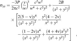 $${{\rm{\sigma }}_{yy}} = \,{{ - 3P} \over {2{\rm{\pi }}{c^2}}}{( {{y \over w}} )^{3}}{{{c^2}{w^2}} \over {{w^4} + {c^2}{y^2}}} + {{2B} \over {{{({x^2} + {y^2})}^{{3 \over 2}}}}}[ {{{2(5 - {\rm{\nu }}){y^4}} \over {{{({x^2} + {y^2})}^2}}} - {{{y^2}(4 - 2{\rm{\nu }})} \over {{x^2} + {y^2}}} - {{(1 - 2{\rm{\nu }}){x^4}} \over {{{({x^2} + {y^2})}^2}}} + {{(4 + 4{\rm{\nu }}){x^2}{y^2}} \over {{{({x^2} + {y^2})}^2}}} ]\quad ,$$
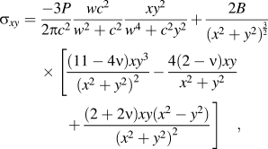 $${{\rm{\sigma }}_{xy}} = \,{{ - 3P} \over {2{\rm{\pi }}{c^2}}}{{w{c^2}} \over {{w^2} + {c^2}}}{{x{y^2}} \over {{w^4} + {c^2}{y^2}}} + {{2B} \over {{{({x^2} + {y^2})}^{{3 \over 2}}}}}[ {{{(11 - 4{\rm{\nu }})x{y^3}} \over {{{({x^2} + {y^2})}^2}}} - {{4(2 - {\rm{\nu }})xy} \over {{x^2} + {y^2}}} + {{(2 + 2{\rm{\nu }})xy({x^2} - {y^2})} \over {{{({x^2} + {y^2})}^2}}} ]\quad ,$$
where  $w = \sqrt {{{({x^2} \,+ \,{y^2} \,- \,{c^2}) \,+ \,\sqrt {{{({x^2} \,+ \,{y^2} \,- \,{c^2})}^2} \,+ \,4{c^2}{y^2}} } \over 2}}$, parameter B denotes the strength of blister-field (residual stress field) which is determined byReference Feng, Qu, Huang and Nix58,Reference Feng, Qu, Huang and Nix59 :
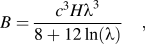 $$B = {{{c^3}H{{\rm{\lambda }}^3}} \over {8 + 12\ln ({\rm{\lambda }})}}\quad ,$$
 $$\lambda = {\left[ {{{8(1 - 2{\rm{\nu }}) + \sqrt 3 {E_{\rm{r}}}/[{{\rm{\sigma }}_{y0}}\tan ({\rm{\alpha }})]} \over {12(1 - 2{\rm{\nu }})}}} \right]^{{1 \over 3}}}\quad ,$$
 $$c = \sqrt {{P \over {{\rm{\pi }}H}}} \quad ,$$
where H is the hardness, E r is the reduced modulus in contact mechanics, σy0 is the yield strength of the material, and d is the plastic zone size.
Finally, the substitution of Eqs. (3), (4), and (10) into Eqs. (1) and (2) yields the nucleation criterion of a Shockley partial dislocation dipole and a stacking fault band with length s.
The plastic zone size d is an important factor for calculating the critical indentation load, which can be given asReference Feng, Qu, Huang and Nix58,Reference Feng, Qu, Huang and Nix59 :
 $$d = {\rm{\lambda }}\sqrt {{P \over {{\rm{\pi }}H}}} = \sqrt {{P \over {{\rm{\pi }}H}}} {\left[ {{{8(1 - 2{\rm{\nu }}) + \sqrt 3 {E_{\rm{r}}}/[{{\rm{\sigma }}_{y0}}\tan ({\rm{\alpha }})]} \over {12(1 - 2{\rm{\nu }})}}} \right]^{{1 \over 3}}}\quad \!\!\!\!,$$
Thus, Eq. (17) implies that the plastic zone size is determined by the indentation load, material properties, and indenter geometry.
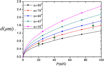
Figure 3 shows the effect of the half apex angle α of the indenter on d, predicted by Eq. (17). It shows that a sharp indenter (i.e., a smaller α) leads to a relatively larger plastic zone size in a given material. In the figure, the green rectangles denote the approximate experimental values of phase transformation zone depth. It is seen that the theoretically predicted plastic zone size coincides very well with experimentally measured depth of phase transformation zone. (Note that the only set of experimental measurements available in the literature is with α ≈ 70°Reference Zhang and Zarudi11,Reference Zarudi and Zhang13,Reference Zarudi, Zhang, Cheong and Yu26 ).
The effect of the indenter geometry on the plastic zone size.

IV. RESULTS AND DISCUSSION
Let us now discuss the critical indentation load P cr for emission of the Shockley partial dislocation from the interface of the amorphous phase and the crystalline silicon. For the silicon material to be studied,Reference Chang and Zhang19 we have G = 80 GPa, ν = 0.22, σy0 = 4 GPa, H = 12.5 GPa, a = 0.542 nm, and γst = 50 mJ/m2.
Previous studies have showed that the plastic deformation in silicon is due to indentation-induced phase transformation and the dislocation-induced ductility due to the extremely high pressure achieved under the tip.Reference Gassilloud, Ballif, Gasser, Buerki and Michler39 Under the ultra-low load nanoindentation, Chang and ZhangReference Chang and Zhang19 demonstrated that silicon was perfectly elastic up to the maximum indentation load of 0.1 mN. This result was well supported by the cross-sectional TEM examination after the indentation test and showed that the subsurface structure of the specimen was damage-free. With a slow loading process, when the indentation load P is about 0.12–0.16 mN, pop-in occurs. The pop-in events are reasonably repeatable, which represents the transition from purely elastic deformation to elastic–plastic deformation, and is the onset of phase transition. As described in the previous section about our model establishment, it is rational to consider that a Shockley partial dislocation can emit after a pop-in has taken place. The emission of the partial dislocation from the interface is energetically favorable and occurs without any energy barrier if the nanoindentation load satisfies P ≥ P cr, where P cr is given analytically by ΔW(s = 2r 0) ≤ 0.Reference Ovid’ko and Skiba50,Reference Bobylev, Mukherjeeb and Ovid’ko51
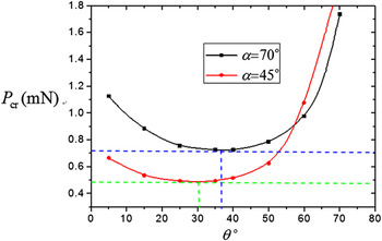
The critical indentation load P cr for dislocation emission as a function of angle θ is shown in Fig. 4 with different half apex angle α of the indenter. It can be seen that P cr has its minimum value corresponding to the most probable location of a partial dislocation emission along the crystallographic plane. This figure therefore derives that for the case of α = 70°, the critical indentation load P cr is about 0.7 mN and the most probable angle θ is about 36° and that for the case of α = 45°, P cr is about 0.5 mN and the most probable θ is about 30°. The evaluation of Gassilloud et al.Reference Lorenz, Zeckzer, Hilpert, Grau, Johansen and Leipner38 showed that the critical load P cr for the first full dislocation generation is equal to or greater than 1.4 mN under scratching by using a blunt Berkovich indenter with a tip radius of 3 μm. The difference between our work and Gassilloud et al.Reference Gassilloud, Ballif, Gasser, Buerki and Michler39 may be attributed to the geometry of the indenter and the type of dislocations (Gassilloud et al.Reference Gassilloud, Ballif, Gasser, Buerki and Michler39 investigated the generation of a full dislocation).
The critical indentation load P cr for dislocation emission as a function of angle θ for α = 70° and α = 45°.

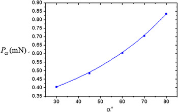
The variation of the critical indentation load P cr versus the half apex angle α of the indenter is depicted in Fig. 5 with θ = 36°. It can be seen that a sharp indenter leads to a relatively smaller P cr. For instance, P cr = 0.4 mN when α = 30°.
The critical indentation load P cr for dislocation emission as a function of angle α for θ = 36°.

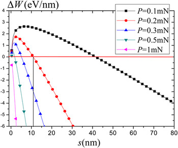
The variation of the energy change ΔW versus the length of stacking fault band s is depicted in Fig. 6 with different values of the indentation load P(θ = 36° and α = 70°). It can be seen that when P is small, such as 0.2 mN, there is an energy barrier at s < 11 nm and the emission of the Shockley partial dislocation is energetically unfavorable under this load. In other words, if a dipole of Shockley partial dislocations has nucleated and if the stacking fault length s reaches 11 nm, the negative partial dislocation will start to slip along the crystallographic plane under the indentation load P = 0.2 mN. When P = 1 mN, ΔW is always negative, indicating that in this case, the emission of the partial dislocation from the interface is always energetically favorable. It can therefore deduct that P = 1 mN is greater than P cr ≈ 0.7 mN, and therefore the emission of the partial dislocation can occur freely without any energy barrier.
The variation of the energy change ΔW versus the length of stacking fault band s.

According to the nanoindentation experiments under an ultra-low range of loads, pop-in occurs when the indentation load P is about 0.12–0.16 mN by using a Berkovich indenter with a tip radius of 227 nm,Reference Bradby, Williams, Wong-Leung, Swain and Munroe22 and P is about 0.3–0.4 mN by using a conical diamond indenter with a tip radius of 1 μm.Reference Wu, Huang, Zou and Dell40 Based on the analysis in Figs. 4–6, the critical indentation load P cr for emission of partial dislocations is about 0.7 mN and is always greater than the load P at pop-in. We can thus conclude that the emission of a partial dislocation is after the pop-in. In other words, the initial inelastic deformation in silicon under nanoindentation is caused by the phase transformation rather than the dislocation of the crystal lattice.
V. CONCLUSIONS
This paper has established a theoretical model to study the critical indentation load condition for the emission of a partial dislocation in silicon under nanoindentation. In the framework of the model, a phase transformation takes place first during nanoindentation. A partial dislocation then emits from the interface between the phase transformation zone and the crystalline silicon when the indentation load reaches a critical value. The emission process represents the generation of a dipole of Shockley partial dislocations. One partial dislocation of the dipole under consideration is immobile (it is located at the interface), whereas the other partial dislocation moves into the bulk of silicon. The mobile partial dislocation slips along a crystallographic plane, and a stacking fault is formed in its wake. Based on the energy criterion, the critical indentation load for the dislocation emission has been derived. The effects of the indenter geometry and the location of dislocation nucleation on the critical indentation load have also been investigated. Some major conclusions from this study are given bellow:
(1) The model prediction showed that a sharp indenter (smaller α) leads to a relatively smaller critical indentation load P cr for emitting a partial dislocation from the interface between the phase transformed zone and the crystalline silicon. For example, the P cr is about 0.7 mN when α = 70° and becomes 0.5 mN when α = 45°.
(2) The emission location of a partial dislocation, θ, varies with α too. When α = 70°, θ is about 36°, which becomes 30° when α = 45°.
(3) If an indentation load P is greater than the critical load P cr, the emission occurs freely as a barrierless process. Otherwise, a partial dislocation can only slip along the crystallographic plane when the dipole of partial dislocations has formed previously and when the length of stacking fault strip has reached a certain value.
(4) This paper shows that the critical indentation load for emission of partial dislocations is always greater than the pop-in load. Thus, the emission of partial dislocations is always after a pop-in and the initial inelastic deformation in silicon under nanoindentation is solely caused by the phase transformation rather than a dislocation.
ACKNOWLEDGMENTS
The authors would like to appreciate the financial support from the Australian Research Council, the NNSFC (Grant Nos. 11172094 and 11172095) and the NCET-11-0122. This work was also supported by Hunan Provincial Natural Science Foundation for Creative Research Groups of China (Grant No. 12JJ7001).