












Introduction
Microwave power transfer (MPT) has emerged as a promising technique for long-distance wireless energy delivery in applications such as space solar power satellites, high-altitude platforms, unmanned aerial vehicle recharging, electric transportation, and large-scale sensor networks [Reference Glaser1–Reference Smyth, Khoshniyat, Barati, Clark, Mirzavand and Iyer6]. In addition to enabling long-range transmission, wireless power offers inherent advantages in safety, reliability, and system flexibility, eliminating mechanical connectors and reducing maintenance in environments where wired infrastructure is impractical or unsafe [Reference Zhang, Pang, Georgiadis and Cecati7]. These attributes are particularly attractive for next-generation electrified transportation, distributed automation systems, and mission-critical platforms, where continuous and contactless power delivery is essential.
Within these systems, the rectifier is the critical interface that governs both the achievable RF-to-DC efficiency and the maximum deliverable power. As MPT systems increasingly target multi-watt and high-frequency operation, the demand for rectifiers that can simultaneously achieve high efficiency, high power-handling capability, and robust performance under large-signal excitation has intensified [Reference Neininger, John, Zink, Meder, Kuri, Tessmann, Friesicke, Mikulla, Quay and Zwick8–Reference Jing, Zhong, Wang and You10].
Most reported high-power rectifiers operate within traditional ISM (Industrial, scientific, and medical) bands (e.g.,  $0.9$,
 $2.45$, and
 $5.8~\text{GHz}$) owing to device maturity and relaxed regulatory constraints [Reference Yu11–Reference Salamin and Zugari13]. However, at these lower frequencies, the achievable power density is fundamentally constrained by antenna aperture scaling and link-budget limitations. Moving to millimeter-wave (mmWave) frequencies can alleviate these constraints by enabling significantly smaller apertures and higher beam directivity [Reference Andersen and Frandsen14, Reference Skrivervik, Bosiljevac and Sipus15]. Nonetheless, mmWave rectification suffers from severe efficiency degradation, strong parasitic effects, and increased design complexity, particularly under high-power operation [Reference Kazemi16–Reference Rangan, Rappaport and Erkip19].
These trade-offs render the X-band ( $8$–
 $12\,\text{GHz}$) an attractive operating region that offers a favorable balance between aperture compactness, beam sharpness, and practically achievable rectification efficiency for multi-watt rectifying front-ends [Reference Shin, Seo, Choi, So and Cheon20]. However, meeting the efficiency and power-handling requirements in this band imposes stringent demands on the rectifying device, including a high diode cutoff frequency, strong breakdown capability, and good electrical and thermal stability.
Conventional Schottky diode technologies struggle to satisfy these requirements. Silicon (Si) and gallium arsenide (GaAs) diodes exhibit an inherent cutoff-frequency–breakdown-voltage ( $\,f_{\mathrm{c}}$–
 $V_{\mathrm{br}}$) trade-off [Reference Zhao, Kang, Zheng, Wu, Huang, Sun, Deng, Wei and Liu21, Reference Zhu, Cao, Xiong, Duan, Turner, Jeng, Xie and Fay22]. Devices optimized for high-frequency operation typically suffer from limited voltage handling capability, whereas high-voltage variants exhibit increased junction capacitance (
 $C_{j}$) and on-state resistance (
 $R_{\mathrm{on}}$), leading to severe efficiency degradation as the operating frequency approaches the X-band region. Consequently, most reported X-band rectifiers either remain in the sub-watt regime or exhibit pronounced efficiency degradation under multi-watt incident power.
Gallium nitride (GaN) Schottky diodes offer a promising pathway to overcome these limitations. Benefiting from GaN’s wide bandgap, high electron mobility, thermal reliability, and strong two-dimensional electron gas (2DEG) confinement, GaN diodes can simultaneously deliver low  $C_{j}$, low
 $R_{\mathrm{on}}$, and high
 $V_{\mathrm{br}}$, making them inherently suitable for high-power, high-frequency rectification [Reference Shao, Fan, Li, Chen, Zhou, Liu, Guo, Xu, Tao and Xie23–Reference Murukesan, Efthymiou and Udrea25].
However, achieving efficient watt-level operation at X-band requires more than device-level performance alone. The diode’s nonlinear conduction and charge-storage behavior strongly interact with the harmonic boundary conditions imposed by the matching network. As a result, a systematic device–circuit co-design methodology is essential to fully leverage GaN’s material advantages and to realize practical Class-F waveform shaping under large-signal excitation.
In this work, we present an X-band GaN Schottky diode rectifier developed within a systematic device–circuit co-design framework. A preliminary version of this work was reported in the EuMW 2025 Proceedings [Reference Yu, Wang, Yang, Hsu, Yen, He, Song, Huang and Zhou26]. The main contributions of this paper are summarized as follows:
(1) A targeted optimization of a custom GaN Schottky diode is proposed for watt-level X-band rectification. Rather than employing a standard topology in isolation, a coordinated design of the multi-finger Y-shaped anode geometry is developed to alleviate current crowding and reduce effective series resistance. Furthermore, the anode-to-cathode spacing, passivation, and field-management strategies are jointly optimized to balance the on-resistance, parasitic capacitance, and reverse-voltage margin, achieving a zero-bias junction capacitance of
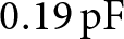
 $C_{j0}=0.19\,\text{pF}$,
$R_{\mathrm{on}}=11\,\Omega$, and
$V_{\mathrm{br}}=205\,\text{V}$. These extracted device characteristics are subsequently incorporated into the harmonic-termination design of the X-band rectifier, thereby establishing the device–circuit co-design methodology of this work. Device reliability is confirmed through stable operation at 350 K and a 24-h continuous stress test.
(2) A 10-GHz practical Class-F harmonic-terminated rectifier is realized by jointly optimizing the microstrip harmonic-termination network with the Schottky diode’s extracted nonlinear characteristics, enabling precise control of the second- and third-harmonic impedances.
(3) The proposed rectifier achieves a peak RF-to-DC conversion efficiency of
$62.1\%$ at an input power of
$37.5\,\text{dBm}$ (
$5.6\,\text{W}$), thereby demonstrating the feasibility of watt-level X-band rectification using the proposed device–circuit co-design approach.


The core contribution of this work lies in the device–circuit co-design of a custom GaN Schottky diode rectifier for watt-level X-band operation. Building upon our preliminary conference report [Reference Yu, Wang, Yang, Hsu, Yen, He, Song, Huang and Zhou26], this paper further includes extended device characterization, thermal and stress reliability verification, large-signal impedance-guided matching, full-wave electromagnetic (EM) circuit co-simulation, and load-dependent RF measurements.
The remainder of this paper is organized as follows. “GaN Schottky diode” section presents the GaN Schottky diode design and characterization. “X-band rectifier with harmonic termination synthesis” section details the practical Class-F harmonic-terminated rectifier co-design methodology and implementation, and discusses the measurement results. “Conclusion” section concludes the paper.
GaN Schottky diode
This section presents a custom GaN Schottky diode that utilizes an optimized lateral architecture with a multi-finger, Y-shaped anode to maximize the periphery-to-area ratio and thus reduce series resistance and current crowding. Fabricated on a high-resistivity GaN-on-SiC substrate, the diode incorporates robust surface passivation and a field-plate-like structure to control electric field peaks and enhance breakdown characteristics. The epitaxial stack, geometric layout, and static DC performance are detailed as follows.
Diode design and fabrication
To systematically determine the final structural dimensions for the target X-band frequency and GaN process, a device–circuit co-design flow was established. First, the required electrical window was defined based on the X-band watt-level rectification requirements: a low  $C_j$ is essential to limit high-frequency capacitive losses, a sufficiently low
 $R_{\mathrm{on}}$ is required for efficient forward conduction, and a high
 $V_{br}$ is mandatory to sustain large RF voltage swings. Guided by these boundary conditions, key geometrical parameters, including the anode finger dimensions, the total number of fingers, and the anode-cathode spacing (
 $L_{ac}$) were iteratively adjusted. The extracted nonlinear device characteristics were subsequently evaluated within the circuit environment to validate their suitability for high-efficiency harmonic-terminated rectification.
The GaN Schottky diode was fabricated on a semi-insulating 4H-SiC substrate, selected for its high thermal conductivity and breakdown strength, which are critical for high-power and high-frequency X-band operation. The epitaxial structure, illustrated in the cross-sectional schematic of Fig. 1(a), was grown by metal-organic chemical vapor deposition. The stack consists of a 1  $\unicode{x03BC}$m Fe-doped GaN buffer layer to suppress parasitic conduction and RF dispersion, a 300-nm unintentionally doped (UID) GaN channel layer, and a 16-nm
 $\mathrm{Al}_{0.25}\mathrm{Ga}_{0.75}\mathrm{N}$ barrier layer that induces a high-density 2DEG via polarization effects. The 2DEG enables high electron mobility, which is essential for achieving high switching speeds and low
 $R_{\mathrm{on}}$. A 2-nm UID GaN cap layer was deposited in situ to protect the AlGaN surface during processing, preserving 2DEG integrity and minimizing current collapse.
The cutoff frequency  $f_T$ defines the diode’s ability to operate at high frequencies and is determined by both
 $C_j$ and
 $R_{\mathrm{on}}$:
 \begin{equation}
f_T = \frac{1}{2 \pi C_j R_{\mathrm{on}}}.
\end{equation}
To achieve high  $f_T$, it is necessary to minimize both
 $C_j$ and
 $R_{\mathrm{on}}$. For first-order design intuition, the junction capacitance trend can be approximated using a parallel-plate model [Reference Streetman and Banerjee27]:
 \begin{equation}
C_j = \frac{\epsilon_r \epsilon_0 A}{d}
\end{equation}
where  $ \epsilon_r \approx 9.5 $ for GaN,
 $ \epsilon_0 \approx 8.854 \times 10^{-12}\,\mathrm{F/m} $,
 $A$ is the anode area, and
 $d$ is the depletion width. Reducing the anode area
 $A$ through optimized finger geometry lowers
 $C_j$ and increases
 $f_T$.
The on-resistance  $R_{\mathrm{on}}$ also affects
 $f_T$ and consists of contributions from the channel resistance
 $R_{\mathrm{channel}}$ and the ohmic contact resistance
 $R_{\mathrm{contact}}$:
 \begin{equation}
R_{\mathrm{on}} \approx R_{\mathrm{channel}} + R_{\mathrm{contact}}.
\end{equation}
To reduce  $R_{\mathrm{on}}$ while maintaining a favorable high-frequency figure-of-merit for X-band rectification, a lateral architecture with an optimized anode-cathode spacing
 $L_\mathrm{ac}$ and a multi-finger Y-shaped anode (Fig. 1(b)) is employed. Specifically, the optimization of
 $L_\mathrm{ac}$ involves a critical design trade-off. While reducing
 $L_\mathrm{ac}$ effectively lowers the
 $R_\mathrm{channel}$ and consequently
 $R_\mathrm{\mathrm{on}}$, it inevitably increases the fringing and inter-finger parasitic capacitances while degrading the reverse-voltage margin (
 $V_\mathrm{br}$). Therefore, the structural dimensions are not determined by minimizing
 $R_{\mathrm{on}}$ alone. Instead, the multi-finger geometry and
 $L_\mathrm{ac}$ are carefully coordinated by jointly evaluating the reduction of
 $R_{\mathrm{on}}$, the strict control of
 $C_j$ to limit high-frequency capacitive losses, and the maintenance of a sufficient
 $V_\mathrm{br}$. Furthermore, this Y-shaped configuration is tailored to alleviate electric field crowding and provide a distributed current path. The fundamental characteristics extracted from this optimized structure directly inform the input-matching and harmonic-termination design in the subsequent rectifier circuit. The area-normalized specific on-resistance
 $R_{\mathrm{on,sp}}$, expressed as the resistance–area product, can be written as
 \begin{equation}
R_{\mathrm{on,sp}} \approx R_{\mathrm{on}} A,
\end{equation}
where  $A$ is the total active anode area. This area-normalized quantity facilitates comparison among devices with different geometrical dimensions.
Structure of the proposed GaN Schottky diode: (a) cross-sectional view showing the GaN/AlGaN epitaxial layers, 2DEG channel, SiN passivation, and metal contacts. (b) Top-view layout of the multi-finger anode–cathode geometry with key dimensions. (c) Optical micrograph of the fabricated GaN Schottky diode device.

(1) Long description
Three parts illustrate the structure of a GaN Schottky diode. The first part is a cross-sectional view showing layers from top to bottom: GaN cap, AlGaN barrier, GaN channel, buffer, nucleation layer and semi-insulating SiC substrate. Metal contacts labeled as anode and cathode are positioned on top, with SiN passivation and 2DEG channel indicated. The second part is a top-view layout of the diode, featuring a multi-finger anode-cathode geometry. It includes dimensions labeled as L subscript AC, L subscript anode and L subscript cathode, with a cut line and N equals 2. The third part is an optical micrograph of the fabricated device, showing the physical layout with visible metal contacts and the central diode structure.
High  $V_\mathrm{br}$ is supported by the wide-bandgap GaN material system together with the optimized lateral anode-to-cathode spacing, field-management design, and surface passivation. In the present lateral device, the breakdown voltage is governed by a nonuniform 2D electric-field distribution, including electric-field crowding near the Schottky-anode edge. Therefore, the measured lateral breakdown voltage cannot be accurately described using a simple one-dimensional critical-field–thickness relationship. Device isolation is implemented via multi-energy boron implantation with doses from
 $5\times10^{12}$ to
 $1\times10^{14}\,\mathrm{cm^{-2}}$, confining the current and improving off-state breakdown. A 100-nm SiN
 $_x$ passivation layer deposited by PECVD (Plasma-Enhanced Chemical Vapor Deposition) at 300
 $^\circ$C suppresses surface trapping and current collapse, further supporting high-voltage operation.
Ohmic contact regions are defined by optical lithography and recessed via a Cl $_2$/BCl
 $_3$ inductively coupled plasma etch to access the 2DEG. A Ti/Al/Ni/Au (20/100/25/50 nm) metal stack is deposited by e-beam evaporation and lifted off, followed by annealing at 825
 $^\circ$C for 30 s in N
 $_2$ ambient to form low-resistance ohmic contacts. Y-shaped anode fingers are patterned using high-resolution stepper lithography to alleviate electric field crowding, with final finger length and head width of 0.25 and 0.35
 $\unicode{x03BC}$m, respectively. Ground-signal-ground (GSG) pads are formed with Ti/Au (50/500 nm) for on-wafer DC and RF characterization. Figure 1(b) shows the top-view layout of the device with key dimensions, while Fig. 1(c) presents an optical micrograph of the fabricated GaN Schottky diode prototype.
Diode electrical properties
The DC characteristics of the fabricated GaN Schottky diode were evaluated at 300 K using a semi-automatic probe station and a Keysight B1500A parameter analyzer. Measurements were performed in a GSG configuration on a temperature-controlled stage, with probe alignment ensured via a high-magnification microscope (Fig. 2).
DC characterization setup using a Keysight B1500A parameter analyzer and a microscope-aligned probe station.

Forward current density–voltage ( $J$–
 $V$) characteristics for the proposed two-finger Schottky diode (finger width
 $W = 35\,\unicode{x03BC}$m, anode-cathode spacing
 $L_{\text{ac}} = 1.875\,\unicode{x03BC}$m) are shown in Fig. 3. The turn-on voltage
 $V_{\mathrm{on}}$, defined at
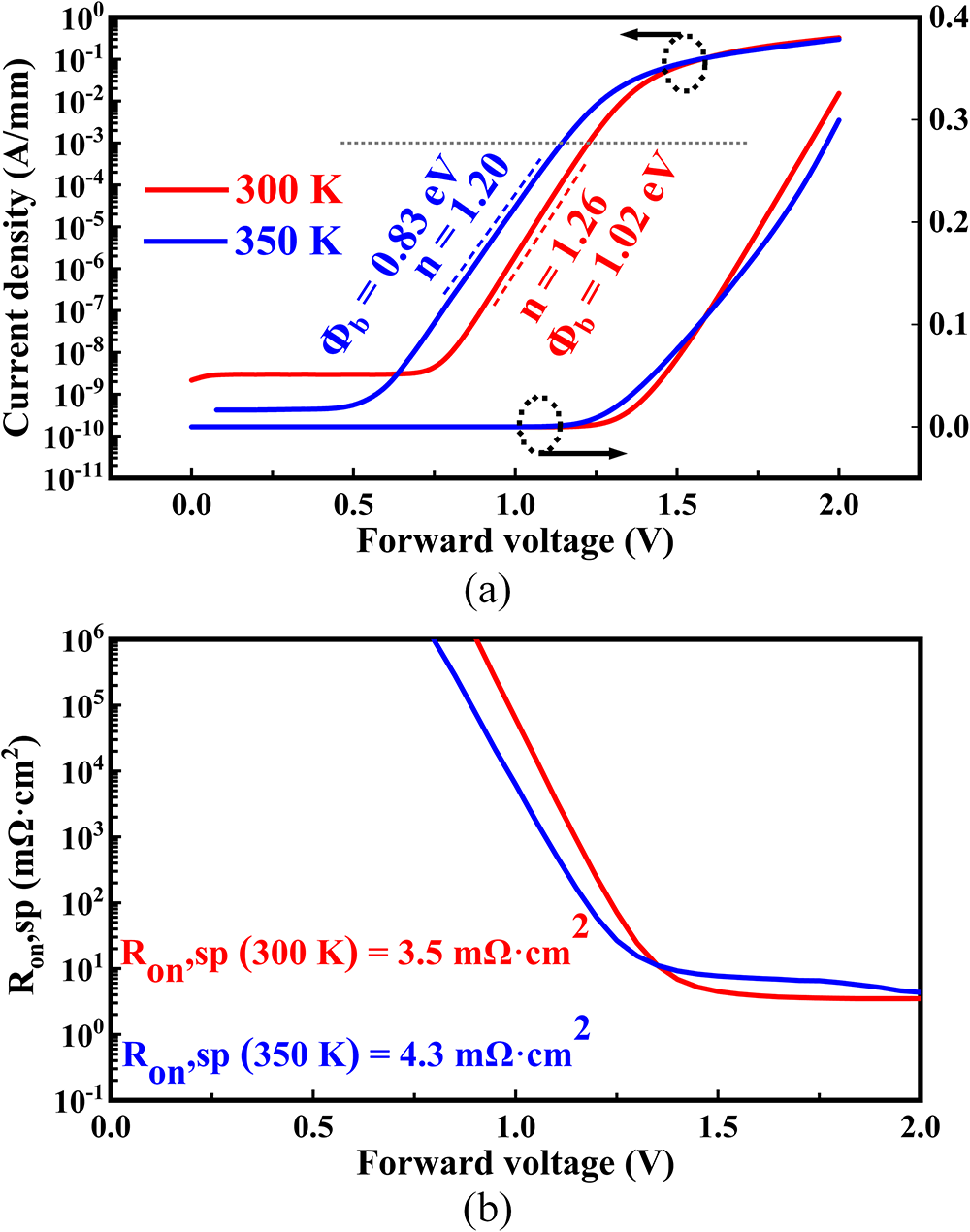
 $J$ = 1 mA/mm, is 1.24 V. At 2 V forward bias, the current density reaches 0.325 A/mm (Fig. 3(a)), corresponding to a specific on-resistance of
 $3.5\,\text{m}\Omega\cdot\text{cm}^2$ (Fig. 3(b)). Sub-threshold analysis yields an ideality factor of 1.26 and a Schottky barrier height of 1.02 eV (
 $\Phi_b$), indicating a high-quality Schottky interface with minimal trap-assisted conduction. In Fig. 3(a), the left
 $y$-axis represents the measured current on a logarithmic scale, whereas the right
 $y$-axis represents the forward current density
 $J$ on a linear scale.
Forward characteristics of the fabricated GaN Schottky diode measured at 300 and 350 K: (a) semilog current–voltage characteristics (left  $y$-axis) and forward current density
 $J$ (right
 $y$-axis), together with the extracted ideality factor and Schottky barrier height; (b) corresponding specific on-resistance
 $R_{\mathrm{on,sp}}$ as a function of forward voltage.

Figure 3 Long description
A line graph with two y-axes and two curves. The x-axis is labeled, Forward voltage (V), ranging from 0.0 to 2.0 in increments of 0.5. The left y-axis is labeled, Current density (A mm superscript -1), with logarithmic tick labels 10 superscript -6, 10 superscript -5, 10 superscript -4, 10 superscript -3, 10 superscript -2, 10 superscript -1 and 10 superscript 0. The right y-axis is labeled, Current (A), ranging from 0.0 to 0.4 in increments of 0.1. A legend shows two series: 300 K and 350 K. Both curves stay near the lowest decade up to about 0.5 V, then rise steeply between about 0.8 V and 1.4 V and continue increasing toward 2.0 V. Text annotations near the rising region read, n equals 1.26 and phi subscript b equals 1.02 eV. The image B showing a line graph with two curves. The x-axis is labeled, Forward voltage (V), ranging from 0.0 to 2.0 in increments of 0.5. The y-axis is labeled, R subscript on sp (m ohm centimeter superscript 2), with logarithmic tick labels 10 superscript 0, 10 superscript 1, 10 superscript 2, 10 superscript 3 and 10 superscript 4. A legend shows two series: 300 K and 350 K. Both curves start near 10 superscript 4 at 0.0 V, decrease gradually to about 1.0 V, then drop sharply between about 1.0 V and 1.4 V to near 10 superscript 0 and remain near 10 superscript 0 from about 1.5 V to 2.0 V. Text annotations read, R subscript on sp (300 K) equals 3.5 m ohm centimeter superscript 2 and R subscript on sp (350 K) equals 4.3 m ohm centimeter superscript 2.
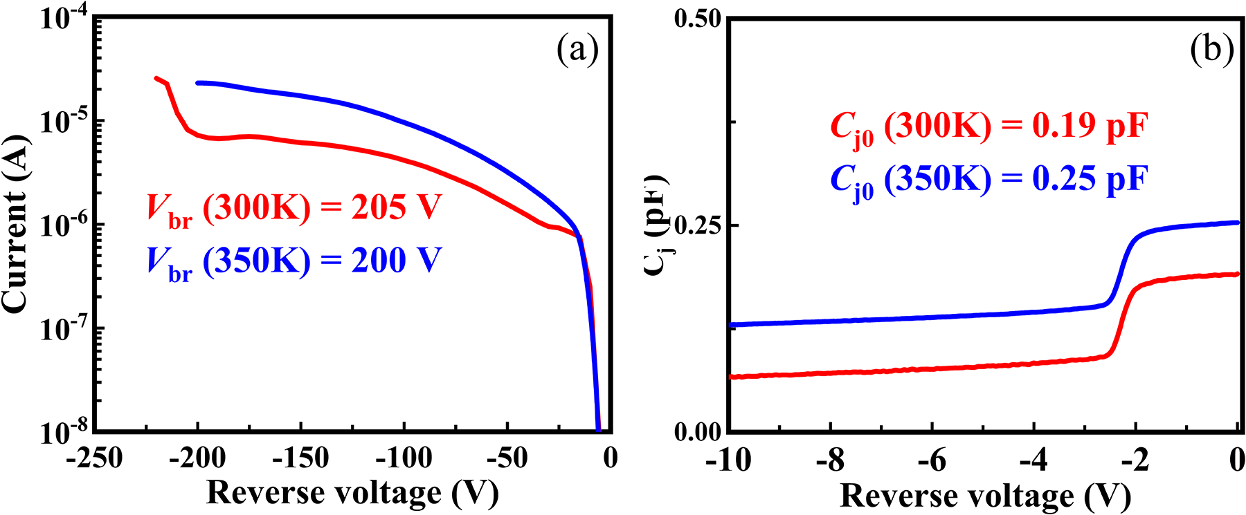
Reverse blocking performance is summarized in Fig. 4. The device exhibits a high  $V_{\mathrm{br}}$ of 205 V, with leakage current below 10
 $\unicode{x03BC}$A across the measured range. A blocking capability of 90–100 V is maintained at only 1
 $\unicode{x03BC}$A leakage (Fig. 4(a)), indicating strong material uniformity and effective field management. Small-signal characterization at 0 V bias reveals an ultra-low
 $C_{\mathrm{j0}}$ of 0.19 pF (Fig. 4(b)).
To better highlight the advantages of the diode proposed in this work, a comparison with representative devices reported in the literature is summarized in Table 1. Compared with other high-frequency Schottky diodes [Reference Dang, Zhan, Zhang, Zhou, Huo, Zhang, Zhang, Ning, Xu and Hao28, Reference Hu, Zhou, Li, Wang, Li, Helaoui and Ghannouchi29], the proposed GaN device demonstrates a well-balanced trade-off among  $C_{j0}$,
 $R_{\mathrm{on}}$, and
 $V_\mathrm{br}$.
Although the device exhibits moderately higher  $C_{j0}$ and
 $R_{\mathrm{on}}$, it achieves a significantly enhanced breakdown voltage, providing a substantially larger reverse voltage margin. This characteristic is particularly beneficial for stable and efficient watt-level rectification at X-band frequencies.
(a) Reverse  $I$–
 $V$ characteristics showing high breakdown voltage and robust blocking at elevated temperature. (b) Junction capacitance versus reverse bias, indicating low and stable capacitance.

Thermal stability was assessed at 350 K, as shown in Figs 3 and 4. The forward characteristics exhibit a predictable shift: current density increases at fixed bias due to higher carrier emission, and  $V_{\mathrm{on}}$ decreases from 1.24 to 1.15 V. Reverse blocking remains robust, sustaining
 $V_{\mathrm{br}}$ = 200 V (instrument limit) with only a moderate leakage increase, indicating stable field distribution. The
 $C_{\mathrm{j0}}$ increases slightly to 0.25 pF, consistent with temperature-induced depletion region narrowing. These trends align with typical behavior of high-quality GaN Schottky diodes and confirm the device’s thermal robustness for high-reliability, high-power, and high-frequency rectification.
Figure 5 shows the behavior of the GaN Schottky diode under continuous  $-$200 V operation. Figure 5(a) presents the current variation over a 24-h period, revealing a slight yet consistent upward trend before eventual stabilization. This behavior reflects the diode’s response to prolonged biasing, with the current gradually approaching a steady-state value over time. Figure 5(b) compares the forward
 $I$–
 $V$ characteristics measured on the fresh device and after 12 and 24 h of continuous
 $-$200 V operation. The curves remain nearly overlapping, exhibiting only minor shifts even after prolonged electrical stress, demonstrating the diode’s excellent stability and robustness under extended high-voltage operation.
Comparison of diode parameters with relevant literature

Table 1 Long description
Columns list reference, material, junction capacitance at zero bias in picofarads, on resistance in ohms, and breakdown voltage in volts. Reference 29 uses GaN with junction capacitance 0.07 pF, on resistance 5.2 ohms, and breakdown voltage 75 V. Reference 30 uses GaAs with junction capacitance 0.02 pF, on resistance 4.0 ohms, and breakdown voltage 7 V. This work uses GaN with junction capacitance 0.19 pF, on resistance 11.0 ohms, and breakdown voltage 205 V.
X-band rectifier with harmonic termination synthesis
Rectifier design
Achieving high conversion efficiency at X-band frequencies is critical for high-power rectification. A major challenge is the temporal overlap between the diode voltage and current waveforms, which increases conduction and switching losses. To minimize this overlap, a practical Class-F harmonic-termination strategy is adopted, in which the second- and third-harmonic impedances are engineered to shape the voltage and current waveforms toward the desired Class-F behavior, thereby reducing the voltage–current overlap integral and enhancing efficiency.
In an ideal Class-F rectifier, even harmonics are short-circuited and odd harmonics are open-circuited, thereby minimizing the voltage–current overlap. In the present work, these Class-F harmonic conditions are used as the design target, while the practical large-signal behavior is influenced by the nonlinear diode conduction and junction-capacitance displacement current at 10 GHz. Approaching this ideal at 10 GHz requires precise device-circuit co-design. The rectifier employs a custom GaN Schottky barrier diode with a low zero-bias junction capacitance  $C_{j0} = 0.19\,\mathrm{pF}$ and a high breakdown voltage
 $V_{\text{br}} = 205\,\mathrm{V}$, which mitigate capacitive losses and provide sufficient voltage headroom to handle high-power signals while maintaining the engineered waveform shapes.
The complete schematic of the proposed X-band practical Class-F harmonic-terminated rectifier is shown in Fig. 6. The circuit is organized into three functional blocks: (1) an input matching network (ML1–ML3), (2) a harmonic termination network (ML4–ML6), and (3) a DC-pass filter with the output load. A DC-blocking capacitor  $C_{\mathrm{block}}$ is included to isolate the DC bias path while allowing RF signal transmission. Microstrip lines are labeled with their characteristic impedances and electrical lengths for accurate design modeling.
(a) Time-dependent current behavior under continuous  $-200\,\mathrm{V}$ bias, indicating a steady increase toward saturation over
 $24$ h. (b) Overlapped forward
 $I$–
 $V$ characteristics measured at fresh,
 $12\,\mathrm{h}$, and
 $24\,\mathrm{h}$, confirming minimal degradation after extended high-voltage operation.

Schematic of the proposed X-band practical Class-F harmonic-terminated GaN rectifier.

Figure 6 Long description
A Class-F GaN rectifier circuit organized into three main blocks. On the left, the input matching network consists of microstrip lines labeled ML1, ML2 and ML3. ML1 has a characteristic impedance of 50 ohms and an electrical length of 50 degrees. ML2 is marked with 120 ohms and 36.7 degrees, while ML3 shows 51.9 ohms and 46.3 degrees. A DC-blocking capacitor, labeled C subscript block, is positioned between ML2 and ML3 to isolate the DC bias path while allowing RF signal transmission. The harmonic termination network is in the center, comprising microstrip lines ML4, ML5 and ML6. ML4 is labeled with 50 ohms and 45 degrees, ML5 with 50 ohms and 30 degrees and ML6 with 50 ohms and 90 degrees. Two red arrows indicate input impedances Z subscript in1 and Z subscript in2. On the right, the DC filter network includes two curved lines labeled with dimensions 3.40 millimeters and 120 degrees and 1.39 millimeters and 120 degrees. The output load is marked as R subscript load. The microstrip transmission line is described with Z for characteristic impedance and E for electrical length. The entire setup is grounded at the top right and the AC source is depicted on the far left.
The rectifier employs a custom GaN Schottky diode, characterized by measured parameters including a turn-on voltage  $V_{\text{on}} = 1.24\,\mathrm{V}$,
 $R_{\mathrm{on}} = 11\,\Omega$,
 $C_{j0} = 0.19\,\mathrm{pF}$, and
 $V_{\text{br}} = 205\,\mathrm{V}$. Furthermore, the extrinsic parasitics introduced by the bonding wires and interconnect pads were incorporated through full-wave EM simulations during the layout design phase, thereby accounting for package-level effects in the circuit implementation. These extracted device parameters, together with extrinsic parasitic effects associated with the implemented layout, bonding wires, interconnect pads, and connector transitions as captured through full-wave EM/circuit co-simulation, are used in the device–circuit co-design. A fully extracted nonlinear intrinsic equivalent-circuit model is beyond the scope of the present work; therefore, the design is framed as a practical harmonic-terminated rectifier developed from measured device characteristics and EM-captured extrinsic parasitics, rather than as an exact ideal Class-F synthesis based on a complete intrinsic model.
Input matching network
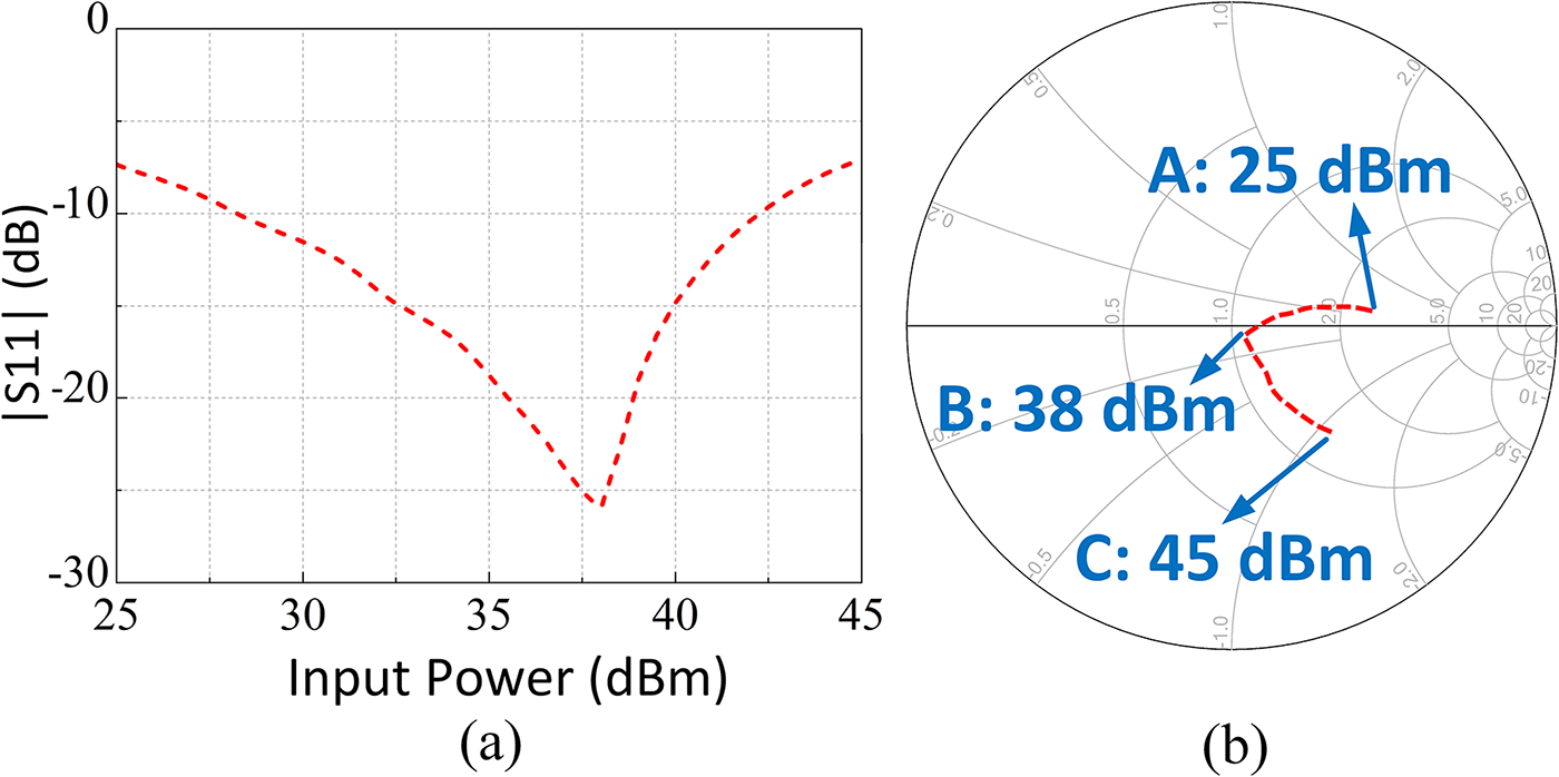
At low input power, the rectifier performance is limited by the high junction resistance ( $R_j$) of the Schottky diode, resulting in increased losses and reduced efficiency. Furthermore, under high-power injection, the diode exhibits severe nonlinearity, causing its dynamic input impedance to deviate significantly from the small-signal state. To address this, the rectifier input behavior under large-signal excitation around the intended operating power (37.5 dBm), together with the extracted device parameters and EM/circuit co-simulation, was used to guide the target matching condition. The input matching network, comprising ML1, ML2, and ML3, was then optimized to approach conjugate matching under this target high-power operating condition. This design effectively compensates for both the device’s inherent large-signal nonlinearity and layout parasitics, maximizing the power transfer.
Figure 7(a) shows the magnitude of the input reflection coefficient, |S11|, in dB versus input power for the fully matched rectifier, and Fig. 7(b) presents the corresponding impedance trajectory on a Smith chart. As the input power increases from 25 dBm (Point A,  $Z_\text{in} = 123.0 + j14.2~\Omega$) to 38 dBm (Point B,
 $Z_\text{in} = 53.9 - j3.5~\Omega$), the impedance moves toward the chart center, achieving near-optimal matching. At 45 dBm (Point C,
 $Z_\text{in} = 67.6 - j54.7~\Omega$), significant capacitive reactance appears due to diode junction modulation under high excitation.
Rectifier input performance versus input power: (a) magnitude of the input reflection coefficient, |S11|, in dB versus input power; (b) input impedance trajectory on a Smith chart for different input power levels.

Harmonic termination network
The harmonic termination network is a critical component of the Class-F harmonic-termination rectifier design [Reference Roberg, Reveyrand, Ramos, Falkenstein and Popovic30]. It utilizes carefully designed microstrip lines of specific electrical lengths to achieve the required impedance conditions at harmonic frequencies. The network consists of three key segments: ML4 ( $\theta = 45^\circ$), ML5 (
 $\theta = 30^\circ$), and ML6 (
 $\theta = 90^\circ$), where
 $\theta$ represents the electrical length at the fundamental frequency
 $f_0$. These segments ensure selective harmonic termination by controlling the impedance at the input and output nodes.
At the second harmonic ( $2f_0$), ML4 (
 $\theta = 90^\circ$) acts as a quarter-wavelength line, which transforms its open-ended termination into a short circuit, yielding
 $Z_{\text{in},1} \approx 0$. Similarly, at the third harmonic (
 $3f_0$), ML5 (
 $\theta = 90^\circ$) also acts as a quarter-wavelength line, producing a short circuit at
 $Z_{\text{in},1}$.
For the second node,  $Z_{\mathrm{in},2}$, the impedance is determined by ML6, where
 $Z_{\mathrm{in},2}$ denotes the transformed impedance at the network reference plane looking toward the diode through ML6 rather than the intrinsic cathode-terminal impedance itself. At the second harmonic (
 $2f_0$), ML6 (
 $\theta = 180^\circ$) acts as a half-wavelength line, replicating the short circuit at
 $Z_{\text{in},1}$, while at the third harmonic (
 $3f_0$), ML6 (
 $\theta = 270^\circ$) functions as a quarter-wavelength line, which transforms the short circuit into an open circuit. The simulated time-domain voltage and current waveforms in Fig. 8 illustrate the intended harmonic shaping, showing reduced voltage–current overlap and efficient power conversion.
Simulated time-domain voltage and current waveforms of the diode rectifier, illustrating practical Class-F harmonic shaping with reduced voltage–current overlap across an input power range of 25–45 dBm.

Figure 8 Long description
Multiple overlaid traces. The horizontal axis is labeled, Time (ps), with tick labels at minus 20, 0, 20, 40, 60, 80, 100, 120, 140, 160, 180 and 200. The left vertical axis is labeled, Vd (V), with tick labels at 0, 20, 40, 60, 80, 100, 120 and 140. The right vertical axis is labeled, Id (A), with tick labels at minus 0.8, minus 0.6, minus 0.4, minus 0.2, 0.0, 0.2, 0.4, 0.6, 0.8, 1.0, 1.2, 1.4, 1.6, 1.8 and 2.0. A set of voltage traces forms repeated high plateaus and low intervals across the time range, with two main high regions centered roughly around 40 to 70 and 130 to 160 on the time axis. A set of current traces forms oscillating wave shapes across the same time range, with alternating positive and negative portions. A vertical double headed arrow near the center of the plot is labeled, 38 dBm.
DC-pass filter
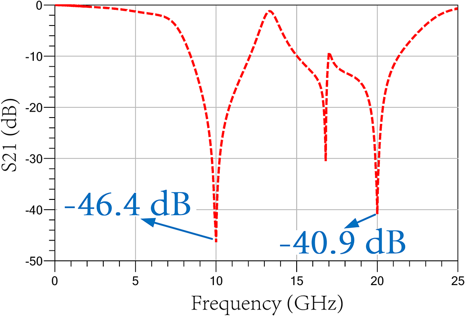
The DC-pass filter is designed to short-circuit the RF energy at 10 GHz ( $f_0$) and its harmonics to ground, ensuring a pure DC output. In this design, to minimize parasitic effects at X-band, two shunt open-circuited radial stubs (with dimensions of 3.40 and 1.39 mm, as shown in Fig. 6) are employed instead of lumped components. These radial stubs provide a broadband, low-impedance RF short, effectively isolating the RF signal from the DC load.
Frequency-domain simulations of the filter performance are shown in Fig. 9, where the transmission coefficient  $S_{21}$ exhibits strong rejection at both the fundamental and harmonic frequencies, with attenuations of
 $-46.4\,\mathrm{dB}$ at 10 GHz and
 $-40.9\,\mathrm{dB}$ at 20 GHz. These results confirm that unwanted RF components are effectively suppressed, enabling efficient extraction of rectified DC power.
Simulated performance of the DC-pass filter, demonstrating strong attenuation at both the fundamental and harmonic frequencies.

Photograph of the fabricated X-band Class-F harmonic-terminated rectifier.

Figure 10 Long description
An X-band Class-F harmonic-terminated rectifier with several labeled components. On the left, the input matching section is marked, leading to an SMA connector. Adjacent to this, the Class-F network is highlighted, followed by the diode positioned centrally. To the right, a heatsink is attached, with a load labeled as R subscript load. Below the load, a DC filter is indicated. The entire setup is mounted on a substrate measuring 46.08 millimeters in width and 23.50 millimeters in height.
Prototype implementation and validation
The fabricated X-band practical Class-F harmonic-terminated rectifier prototype is shown in Fig. 10, with the GaN Schottky diode mounted at the junction of the harmonic termination network. The rectifier is fabricated on a 1.6-mm-thick Rogers 3003 substrate ( $\varepsilon_r = 3.00$,
 $\tan\delta = 0.0010$ at 10 GHz), chosen for low loss and high power-handling capability at X-band.
Microwave-to-DC conversion efficiency and output voltage of the X-band Class-F harmonic-terminated rectifier: (a) efficiency versus input power at 10 GHz, (b) efficiency and output voltage versus frequency at  $37.5\,\mathrm{dBm}$, and (c) efficiency and output voltage versus load resistance at 10 GHz and
 $37.5\,\mathrm{dBm}$.

Figure 11 Long description
Three multi-line graphs labeled (a), (b) and (c) related to the X-band Class-F harmonic-terminated rectifier. Graph (a) shows efficiency and output voltage versus input power in decibel-milliwatts (dBm). The x-axis ranges from 25 to 45 dBm and the y-axis displays efficiency in percent and voltage in volts. Two lines are present: the solid line represents simulation data and the dashed line represents measurement data. The peak efficiency is 62.1 percent at 37.5 dBm. The simulation line shows a gradual decline in efficiency beyond this point, while the measurement line shows a sharper drop. Graph (b) presents efficiency and output voltage versus frequency in gigahertz (GHz), with the x-axis ranging from 9.2 to 10.8 GHz. The y-axis shows efficiency in percent and voltage in volts. The solid line indicates simulation data, peaking at 10 GHz, while the dashed line represents measurement data, showing a similar peak but with slight variations across the frequency range. Graph (c) depicts efficiency and output voltage versus load resistance in ohms, with the x-axis ranging from 300 to 800 ohms. The y-axis displays efficiency in percent and voltage in volts. The solid line for simulation data peaks around 500 ohms, while the dashed line for measurement data shows a similar trend but with differences in peak values. These graphs demonstrate the performance sensitivity of the rectifier to input power, frequency and load resistance, highlighting areas where simulation and measurement data align or diverge.
X-band rectifier performance comparison

Table 2 Long description
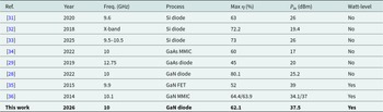
Rows compare rectifier references by year, frequency in gigahertz, process, maximum efficiency in percent, input power in dBm, and whether the design is marked watt level. Si diode entries list 2020 at 9.6 GHz with 63 percent max efficiency and 26 dBm input, 2018 at X band with 72.2 percent and 19.4 dBm, and 2025 at 9.5 to 10.5 GHz with 73 percent and 26 dBm, all marked not watt level. A GaAs MMIC entry in 2022 at 10 GHz reports 60 percent max efficiency at 17 dBm, not watt level, and a GaAs diode entry in 2019 at 12.75 GHz reports 45 percent at 20 dBm, not watt level. GaN entries include a 2022 GaN diode at 10 GHz with 80.1 percent max efficiency at 25.2 dBm, not watt level. Watt level entries are 2015 GaN FET at 9.9 GHz with 52 percent at 39 dBm, 2014 GaN MMIC at 10.1 GHz with two max efficiency values 64.4 percent and 63.9 percent paired with two input powers 34.1 dBm and 37 dBm, and a 2026 GaN diode at 10 GHz with 62.1 percent at 37.5 dBm.
To ensure robust implementation of the intended Class-F harmonic boundary conditions, the final layout dimensions were iteratively fine-tuned through full-wave EM and circuit co-simulations. This optimization process specifically accounted for fabrication tolerances, microstrip-to-SMA (SubMiniature version A) connector launches, and the previously discussed diode bonding parasitics. By incorporating these practical discontinuities into the harmonic network synthesis, the phase requirements for ML4–ML6 were preserved at  $f_0$,
 $2f_0$, and
 $3f_0$, thereby enabling the intended voltage and current waveform shaping for high-efficiency operation. Consequently, the reported measured efficiencies inherently encompass these practical loss mechanisms and parasitic effects, representing a realistic assessment of the overall system performance.
The RF-to-DC conversion efficiency  $\eta$ is defined as
 \begin{equation}
\eta = \frac{V_{\text{out}}^2}{R_{\text{load}} P_{\text{in}}}
\end{equation}
where  $V_\mathrm{out}$ is the DC voltage across the load
 $R_\mathrm{load}$ and
 $P_\mathrm{in}$ is the available RF power referenced to the SMA input plane.
The experimental performance was characterized using a signal generator followed by a high-power driver amplifier to provide the required RF input levels. To ensure measurement accuracy, the input power was determined through a pre-calibration procedure using a high-precision power meter to measure the available power at the SMA connector reference plane, thereby accounting for cable and connector losses. By defining  $P_\mathrm{in}$ as the available power at the SMA reference plane, the reported efficiency naturally includes the source–rectifier mismatch loss, thereby providing a conservative and realistic assessment of the overall system performance. During testing, the rectifier was mounted on a fan-assisted heatsink under room-temperature laboratory conditions to facilitate heat dissipation and maintain stable operation. The output DC voltage was monitored using a digital voltmeter.
Figure 11 presents the measured and simulated performance. In Fig. 11(a), the RF-to-DC efficiency and output voltage versus input power are compared. A peak efficiency of 62.1% is achieved at 37.5 dBm, in good agreement with simulations. As the input power exceeds 37.5 dBm, a gradual decline in the rectification efficiency is observed. As highlighted by the annotated 38-dBm traces in Fig. 8, the simulated diode current increasingly deviates from the intended near-half-sinusoidal waveform at high power and exhibits a larger reverse-current component while the diode voltage approaches its maximum. This waveform degradation, together with increased conduction loss and self-heating, can contribute to additional dissipation and is consistent with the measured efficiency roll-off at high input powers. Figure 11(b) shows the frequency dependence at 37.5 dBm, with the peak measured efficiency occurring at 10 GHz and the efficiency remaining above 40% across 9.2–10.8 GHz.
To justify the selected operating load, the measured RF-to-DC efficiency and output voltage versus load resistance at the target operating condition of 10 GHz and 37.5 dBm are presented in Fig. 11(c). As observed, the rectifier achieves its highest efficiency near  $R_{\mathrm{Load}}=470\,\Omega$, which was therefore selected as the operating load under the target operating condition.
Table 2 provides a comparative benchmark of X-band rectifiers, highlighting the trade-off between efficiency and power-handling capability critical for high-power MPT applications. Si- and GaAs-based rectifiers achieve high efficiencies (up to 73%) but are limited to input powers below approximately 26 dBm (400 MW), restricting their use in high-power scenarios [Reference Hu, Zhou, Li, Wang, Li, Helaoui and Ghannouchi29, Reference Cao, Lin and Liu31–Reference Molles, Robinson, Kwiatkowski and Popović34 ]. In contrast, GaN-based designs leverage superior material properties to enable watt-level operation. While a recent GaN diode design [Reference Dang, Zhan, Zhang, Zhou, Huo, Zhang, Zhang, Ning, Xu and Hao28] achieved 80.1% efficiency, it remained below the watt-level threshold. Prior GaN FET (Field-Effect Transistor) and MMIC (Monolithic Microwave Integrated Circuit) rectifiers, [Reference Schafer, Coffey and Popović35, Reference Litchfield, Schafer, Reveyrand and Popović36] have demonstrated power handling above 34 dBm, but with moderate efficiencies (52–64%).
The proposed rectifier operates at 10 GHz and achieves a measured peak RF-to-DC efficiency of 62.1% at an input power of 37.5 dBm (5.6 W). Although the absolute efficiency is not the highest among all reported X-band rectifiers, the result demonstrates that a diode-based GaN implementation can be extended into the watt-level regime while maintaining competitive conversion efficiency. This provides useful evidence for practical high-power X-band MPT front-end design.
Conclusion
In conclusion, this work demonstrates an experimentally verified device–circuit co-design methodology for an X-band watt-level GaN diode rectifier. Specifically, the results show that (1) a custom GaN Schottky diode can be structurally tailored to jointly achieve low  $C_j$, acceptable
 $R_{\mathrm{on}}$, and high
 $V_{\mathrm{br}}$ for watt-level X-band operation; (2) the extracted device characteristics can be directly incorporated into the harmonic-termination and matching-network design; and (3) this coordinated approach enables reliable and efficient diode-based rectification in a regime where both operating frequency and power handling are challenging.
Competing interests
The authors declare none.

Xiaochen Yu received the M.Sc. (Eng.) degree in integrated circuits, Nanjing, China, in 2018, and the M.Sc. (Eng.) degree in communications from the University of Leeds, Leeds, UK, in 2020. He received the dual Ph.D. degree in wireless power transfer and on-chip systems through a collaborative program at the University of Liverpool, Liverpool, UK, and National Tsing Hua University, Hsinchu, Taiwan, in 2026. His research interests include RF circuits, microwave rectifiers, wireless power transfer, GaN devices, and microwave integrated circuits for wireless and power applications.

Haoran Wang received the B.Sc. degree in applied physics from Dalian University of Technology, Dalian, China, in 2015. He is currently pursuing the Ph.D. degree in microelectronic engineering at the Institute of Electronics Engineering, National Tsing Hua University, Hsinchu, Taiwan. His current research interests include wide-band gap semiconductor-based power and RF devices and circuits.










 Open access

