Introduction
Amorphous oxide semiconductors (AOS) can be deposited over large areas with uniform structural and electrical properties.[Reference Nomura, Ohta, Takagi, Kamiy, Hirano and Hosono1] These materials have received considerable research and industry attention, largely due to optical and electronic properties that make them suitable for transparent thin film transistors (TFTs), a building block for many types of display and interactive electronics.[Reference Nomura, Ohta, Takagi, Kamiy, Hirano and Hosono1] Their flexibility and applicability to wearable electronics has also been demonstrated by numerous research groups.[Reference Nomura, Ohta, Takagi, Kamiy, Hirano and Hosono1, Reference Nomura, Takagi, Kamiya, Ohta, Hirano and Hosono2]
The application of AOS in devices other than transistors, notably memristors and resistive random access memory, is gaining interest. For these devices, the oxide is typically inserted between metallic electrodes to form metal–insulator–metal structures, a two-terminal architecture well suited to implementation within three-dimensional arrays. Combining memristors and transistors for advanced neuromorphic circuits is an exciting prospect and self-programming capabilities have already been demonstrated using Si-based devices.[Reference Borghetti, Li, Straznicky, Li, Ohlberg, Wu, Stewart and Williams3] If these devices and circuits were based on AOS, then transparency, simplified fabrication, and/or flexibility would be added benefits.
Indium-gallium-zinc-oxide (IGZO) is currently the dominant transparent AOS for TFTs but amorphous zinc-tin-oxide (a-ZTO) is a low-cost indium-free alternative. Thin films of a-ZTO have been deposited using numerous methods including chemical vapor deposition,[Reference Dang, Kawaharamura, Furuta and Allen4] conventional physical vapor deposition (PVD),[Reference McDowell, Sanderson and Hill5] and plasma-assisted PVD.[Reference Murdoch, McCulloch and Partridge6] The latter has produced metal oxide layers of sufficient quality for transparent ZnO transistors,[Reference Elzwawi, Kim, Lynam, Mayes, McCulloch, Allen and Partridge7, Reference Rembert, Battaglia, Anders and Javey8] high-K dielectric layers,[Reference Murdoch, Ganesan, McKenzie, Bilek, McCulloch and Partridge9] and more recently, a-ZTO for devices.[Reference Tran, Mayes, Murdoch, McCulloch, McKenzie, Bilek, Holland and Partridge10, Reference Murdoch, McCulloch and Partridge11] Previously, we showed that combined DC and high-power impulse magnetron sputtering (HiPIMS) can produce a-ZTO at moderate growth temperatures with very low unintentional doping and high carrier mobility.[Reference Tran, Mayes, Murdoch, McCulloch, McKenzie, Bilek, Holland and Partridge10] Furthermore, the n-type carrier concentration in this material can be altered controllably by annealing the films in the presence of hydrogen.[Reference Tran, Mayes, Murdoch, McCulloch, McKenzie, Bilek, Holland and Partridge10] As with other AOS, much of the device research performed on a-ZTO has involved TFTs.[Reference Dang, Kawaharamura, Furuta and Allen4, Reference McDowell, Sanderson and Hill5] It has been shown that partially oxidized Ag (AgOx) can form highly rectifying contacts to a-ZTO and that these contacts, when employed as gates in metal-semiconductor field-effect-transistors (MESFET) devices, exhibit high stability under normal operating voltages/fields.[Reference Dang, Kawaharamura, Furuta and Allen4] However, in ZnO MESFETs with AgOx gates, bias stress-induced degradation has been observed and attributed to Ag migration/diffusion into the channel region.[Reference Elzwawi, Hyland, Lynam, Partridge, McCulloch and Allen12]
Electric-field-driven Ag migration has been reported in oxides, oxynitrides, and carbon-based materials.[Reference Wang, Rao, Midya, Joshi, Jiang, Lin, Song, Asapu, Zhuo, Li, Wu, Xia and Joshua Yang13, Reference Longo, Cavalcante, Volanti, Gouveia, Longo, Varela, Orlandi and Andrés14, Reference Wang, Joshi, Savel'ev, Jiang, Midya, Lin, Hu, Ge, Strachan, Li, Wu, Barnell, Li, Xin, Williams, Xia and Yang15] Characteristics observed include emulation of the Ca2+ or Na+ dynamics of a biosynapse in diffusive Ag-in-oxide memristors with Pt/SiOxNy:Ag/Pt structure.[Reference Wang, Joshi, Savel'ev, Jiang, Midya, Lin, Hu, Ge, Strachan, Li, Wu, Barnell, Li, Xin, Williams, Xia and Yang15] Despite reports of similar behavior in AgOx/a-ZTO[Reference Dang, Kawaharamura, Furuta and Allen4] Schottky devices, memristive behavior in these material combinations has received comparatively little attention. Resistive switching has been demonstrated in IGZO[Reference Wang, Xu, Li, Yu, Liu and Zhu16] and a-ZTO[Reference Murali, Rajachidambaram, Han, Chang, Herman and Conley17, Reference Rajachidambaram, Murali, Conley, Golledge and Herman:18] and we recently reported resistive switching and emulation of learning functions in annealed a-ZTO/Ag junctions.[Reference Murdoch, McCulloch and Partridge11] In the latter, electrical characterization suggested the underlying mechanism but direct observation of this mechanism was not possible due to the vertical device architecture. Here, a lateral architecture has been adopted for the devices which has enabled microscopy of the region between the contacts before and after electrical characterization. The existence (or absence) of a filament within the devices can be verified in this way and the underlying switching mechanisms can be better understood.
Methods
The a-ZTO film was co-deposited at 100 °C onto SiO2 and Al2O3 using an AJA four-gun magnetron sputter deposition system and RUP-7 pulsed power supply. Prior to deposition, the system pressure was <1 × 10⁻⁶ Torr. The potential of the substrate floated (at ~10 V) during the 20 min deposition. The Zn and Sn targets were both 3 in. diameter, 99.99% purity, and they were, respectively, operated in HiPIMS mode (with pulse amplitude, width, and frequency of 600 V, 150 µs, and 100 Hz) and in DC magnetron sputtering mode at 75 W. The 1:3 O2:Ar process pressure was 6.0 mTorr. No instabilities occurred during the 20 min reactive deposition process. The resulting film thickness was 70 nm. Further details of similar HiPIMS a-ZTO deposition processes as well as target current/voltage waveforms are reported elsewhere.[Reference Tran, Mayes, Murdoch, McCulloch, McKenzie, Bilek, Holland and Partridge10] Following deposition, the wafers were diced into 10 mm × 10 mm substrates for optical, structural, and electrical characterization followed by device fabrication. X-ray photoelectron spectroscopy (in a K-α system with monochromated Al K-α source) was used to determine the composition. An Asylum Research MFP-3D Infinity atomic force microscope was used to assess surface topography/roughness and measure the film thickness from step-height measurements.
UV-Visible spectroscopy was performed using a Cary 50 UV-Vis spectrometer to determine transparency and optical band-gap. Spectroscopic ellipsometry was performed using a J. A. Woolam M-2000 to determine the refractive index of the a-ZTO. X-ray diffraction using a Bruker D4 in Bragg–Brentano configuration confirmed the amorphous microstructure of the films. Al Van der Pauw contacts were thermally evaporated and electrical measurements using an Ecopia HMS-3000 system revealed the as-deposited 10 mm × 10 mm films to be semi-insulating.
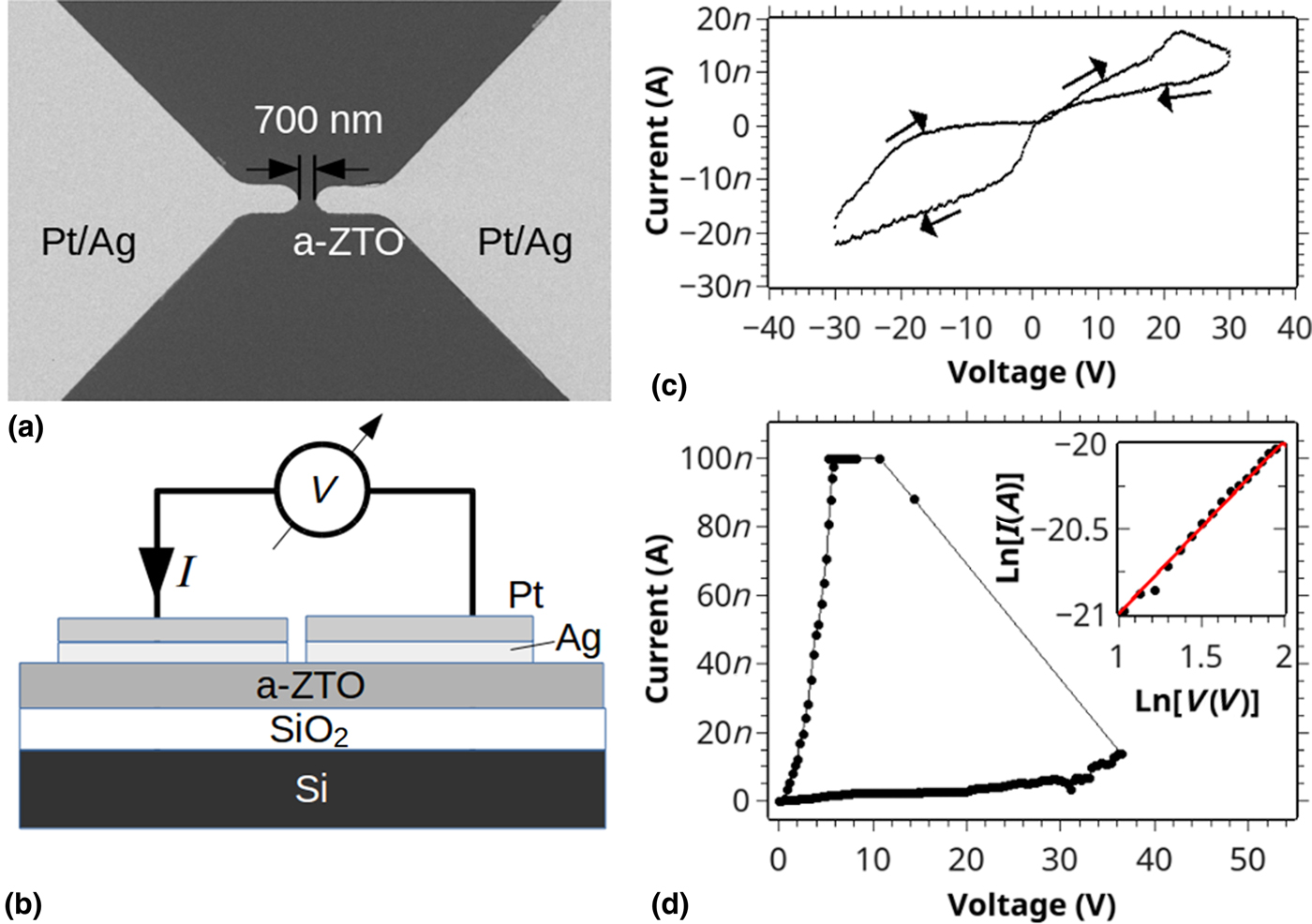
Electron beam lithography was used to pattern PMMA electron-beam resist (950 PMMA A4, thickness 200 nm). A FEI Nova NanoSEM interfaced with Nabity NPGS electron beam writing software was used for this purpose. The operating conditions were: 20.00 kV accelerating voltage, working distance 5 mm, beam current 18 pA. A Gatan PECS ion-beam deposition system was then used for the (first) Ag and (second) Pt device layers (each 30 nm in thickness). The Pt capping layer assisted in providing good contact to the device during probing. An image of the completed device and a schematic representation of the cross-section/measurement circuit are shown in Fig. 1. Out-diffusion of oxygen from the a-ZTO device layer is expected to yield a sub-stoichiometric silver–oxide interface layer. This out-diffusion has been observed in similar devices using transmission electron microscopy and electron energy loss spectroscopy.[Reference Mayes, Partridge, Field, McCulloch, Durbin, Kim and Allen19]
(a) Electron micrograph and (b) cross-sectional schematic representation of the Pt-capped Ag/a-ZTO memristor device. I–V characteristics taken from devices with (c) Pt (only) electrodes and (d) with Ag/Pt electrodes. At low bias in the pristine device state, the slope of the Ln(I) versus Ln(V) plot [inset in (d)] is unity, consistent with transport by direct tunneling.

Room-temperature two-probe current–voltage characteristics were measured on a Keysight twin channel source-measurement unit with the device mounted on a probe station. Finally, a FEI SCIOS electron microscope was used to image the pristine and switched devices. The operating conditions were: 5.00 kV accelerating voltage, working distance 2.9 mm, beam current 200 pA, and substrate bias −4.00 kV.
Results and discussion
The resistivity of the a-ZTO film (with composition Zn:Sn = 44:56) exceeded 10 kΩ.cm. Optical transmission through the 70 nm film exceeded 80% across the visible spectrum and the optical band-gap was 2.9 eV. As-deposited, the device exhibited high resistance at low bias, as shown in the “forming” characteristics of the device in Fig. 1(d). A current limit of 100 nA was imposed during this voltage sweep. Figure 1(c) shows I–V characteristics from a device with identical geometry to that shown in Fig. 1(a) and patterned on the same a-ZTO film but without the Ag device layer. As shown, this Pt-contacted device exhibited I–V hysteresis, suggesting that mobile defects moved under the action of the applied E-field. The markedly different I–V characteristics in Fig. 1(d) come from the device shown in Fig. 1(a) with the Ag device layer. At low bias (below the threshold voltage), the I–V characteristic is approximately linear [see inset Fig. 1(d)]. This is consistent with the characteristics of back-to-back (metal–semiconductor–metal) Schottky diodes, in which emission over the potential barriers is excluded and the dominant carrier transport mechanism is direct tunneling through the potential barriers.[Reference Chiquito, Amorim, Berengue, Araujo, Bernardo and Leite20] With an applied electric field of 0.5 MV/cm, the current (and conductance) increases sharply. This electric field is lower than the 2–4 MV/cm field reported to form a filament in a vertical Al/a-ZTO/Pt structure.[Reference Murali, Rajachidambaram, Han, Chang, Herman and Conley17] Ag is known to diffuse more rapidly in ZnO (with rates of ~1 × 106 cm2/s quoted) than it does in many other oxides used in Ag-filament-based memristors, including TiO2.[Reference Yaqoob and Huang21] However, the relative ion mobilities of Ag and Al in a-ZTO of the composition employed here are unknown.
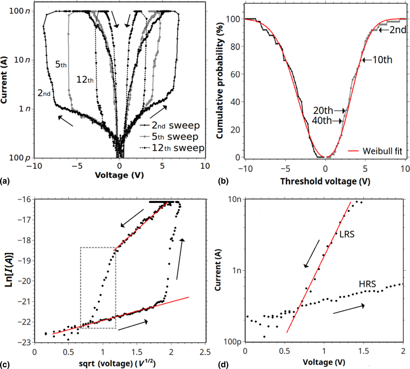
Figure 2(a) shows I–V characteristics measured immediately after the forming step in Fig. 1(d). These measurements, taken with a 100 nA current limit imposed and with one complete sweep taking 18 s, show the pinched hysteresis loop typical of memristors. The switching between the high- and low-resistance states (HRS and LRS) occurs above a threshold for both positive and negative voltages. Figure 2(b) shows the cumulative probability of a switching event as a function of threshold voltage. This plot is approximately symmetric, as expected when the two electrodes are composed of identical materials. The positive and negative threshold voltages reduced with increased operation, as shown in Fig. 2(b) where selected points are labelled with their respective sweep numbers. The cumulative probability versus threshold voltage characteristic can be fitted using the Weibull function[Reference Weibull22, Reference Tappertzhofen and Hofmann23]
 $$F(x) = 1 - \exp \left[ {{\left( { - \displaystyle{x \over {x_o}}} \right)}^\beta} \right],$$
where F is the switching probability, x is a positive/negative voltage, x o is the average value of V threshold, and β is the Weibull slope. The curves on both sides of the origin are fitted well by single values of β, indicating a single conducting pathway (filament).[Reference Tappertzhofen and Hofmann23] At voltages below the switching threshold in the HRS, the I–V relationship can be fitted with the Schottky emission equation [see Fig. 2(c)] as in the work of Murali et al.[Reference Murali, Rajachidambaram, Han, Chang, Herman and Conley17] Using this equation, a slope of 0.91 and a contact separation of 700 nm, yields a relative dielectric permittivity of 3.7. Following the approach of Murali et al.,[Reference Murali, Rajachidambaram, Han, Chang, Herman and Conley17] the high-frequency dielectric permittivity was obtained from the square of the refractive index of the a-ZTO film, measured using spectroscopic ellipsometry. This measurement yielded a relative dielectric permittivity of 3.6. Poole–Frenkel (P–F) emission was excluded as the dominant transport mechanism since the P–F equation provides a less accurate fit to the data and fails to account for asymmetry observed in the low-bias I–V characteristics. Furthermore, the dielectric constant required for best correspondence to our data exceeded any published values for a-ZTO.[Reference Murali, Rajachidambaram, Han, Chang, Herman and Conley17, Reference Rajachidambaram, Murali, Conley, Golledge and Herman:18]
(a) I–V plot taken from the device with 100 nA current limit imposed during measurement and showing hysteresis with (b) cumulative probability plot of positive/negative threshold voltages fitted using Weibull's function.[Reference Weibull22] The positive threshold voltages are shown for the second, tenth, 20th and 40th sweeps. (c) and (d) show fitting of HRS and LRS in the fourth I–V sweep (see main text).

As the current falls below the current limit of 100 nA in the LRS, the I–V characteristics appear to remain consistent with transport by Schottky emission [Fig. 2(c)]. If the relative permittivity of the a-ZTO between the electrodes is assumed constant, a new effective contact separation less than 1/10th the separation between the electrodes can be calculated from this LRS slope. An incomplete filament between the electrodes, containing, for example, gaps and/or inter-granular barriers, could produce this result. Potential barriers existing at the Ag electrodes in the form of AgOx interface layers are also likely. Conductance in the LRS at lower voltages [dashed box in Fig. 2(c)] appears to be limited by Schottky barrier(s) since this region is linear on a semi-logarithmic I–V plot [Fig. 2(d)]. This characteristic is attributed to Schottky barrier(s) at the electrodes and/or at gaps in the filament. After 50 sweeps with a 100 nA current limit imposed, the I–V relationship in the LRS suggested multiple current-limiting mechanisms with an unstable filament leading to volatile behavior. Ohmic conduction was not observed.
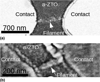
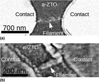
Figure 3(a) shows a back-scattered electron image of the device after the forming sweep shown in Fig. 1(d) and the subsequent sweeps producing the systematic resistive switching shown in Fig. 2. A fragmented filament extends across the a-ZTO layer between the planar Pt-capped Ag electrodes (brightest areas left and right within the image). The contrast between the fragments and surrounding a-ZTO in the image shows that they contain material with higher atomic number. Since Pt is considered inert and is not in direct contact with the a-ZTO, we assert that the filament is rich in Ag. Similar Ag filaments have been observed in memristors based on a variety of oxides using high-resolution transmission electron microscopy,[Reference Longo, Cavalcante, Volanti, Gouveia, Longo, Varela, Orlandi and Andrés14, Reference Wang, Joshi, Savel'ev, Jiang, Midya, Lin, Hu, Ge, Strachan, Li, Wu, Barnell, Li, Xin, Williams, Xia and Yang15] but observation in a scanning electron microscope (SEM) is notable because using solid substrates (not electron-transparent membranes or cross-sectioned specimens) is possible and greatly simplifies fabrication/handling. The filament must reside largely within the a-ZTO layer (sub-surface) since scanning probe microscopy (not shown) revealed no measurable alteration of surface topography in the area between the contacts. Root-mean-square roughness was 0.4 nm before and after operation.
Back-scattered electron image of nanoscale filaments extending between Pt-capped Ag electrodes separated by (a) 700 nm and (b) 200 nm.

Identical Ag/Pt contacts on an amorphous C film with similarly high sheet resistance failed to form a filament with four times the applied electric field, showing that the a-ZTO host layer plays an important role in the device characteristics. As shown in Fig. 1(c), a similar device with Pt contacts (and no Ag layer) patterned on the same a-ZTO film exhibited less significant I–V hysteresis under similar measurement conditions. The current in that device also failed to reach the 100 nA limit imposed. Based on our measurements, it is proposed that a local current path exists between the contacts in the pristine semi-insulating a-ZTO. In a study on Ag migration in TiO2 using density functional theory (DFT),[Reference Prada, Rosa, Giordano, Di Valentin and Pacchioni24] Prada et al. state that mobile defects such as oxygen vacancies are likely to facilitate initial conduction. In a-ZTO transistors with AgOx gates, improved behavior after bias stress has been attributed to the motion of these defects at higher fields.[Reference Dang, Kawaharamura, Furuta and Allen4] We suggest that as the field is increased in the memristor and the current through the local path increases during the forming process, Ag ions migrate along the conduction path with assistance given by Joule heating, vacancy motion, and/or bond rearrangement. This work and preceding work[Reference Dang, Kawaharamura, Furuta and Allen4] suggests that in a-ZTO, as in TiO2,[Reference Prada, Rosa, Giordano, Di Valentin and Pacchioni24] Ag ions are stable. Application of electric field is therefore an effective means to arrange Ag ions/clusters within a-ZTO to form filaments. The DFT calculations of Prada et al. showed steric repulsion of Ag within TiO2, leading the authors to state that amorphization of the host material may assist in further mobilizing Ag ions.[Reference Prada, Rosa, Giordano, Di Valentin and Pacchioni24] Hence, increased ion mobility is expected in a-ZTO and likely to cause faster switching and faster filament relaxation.
Devices with identical layer structure to that shown in Fig. 1(b) but with differing electrode separations were fabricated, operated, and imaged to further investigate the behavior of the conducting Ag filaments in a-ZTO. Due to the presence of the Schottky barriers (and associated potential drops) at the electrode/a-ZTO interfaces, the threshold voltage did not increase linearly with the electrode separation. The threshold voltage range for filaments with lengths 200–700 nm was 24–38 V. The electrical characteristics exhibited by the a-ZTO memristors are consistent with those of nanoscale conducting wires subject to Rayleigh instability.[Reference Toimil Molares, Balogh, Cornelius, Neumann and Trautmann25] Figure 3(b) shows a device with electrodes separated by 200 nm after operation with the same 100 nA current limit and sweep parameters as employed for the device in Fig. 3(a). (The I–V characteristics of this device are shown in Supplementary Fig. S1.) The filament shown in Fig. 3(a) has clearly ruptured and has done so in a manner consistent with the Rayleigh instability condition. The rupture in the shorter filament in Fig. 3(b) is not resolvable in the SEM image, but since this filament also exhibited volatile behavior and was in the HRS before imaging, it is believed to be discontinuous. If the characteristic Rayleigh perturbation wavelength exceeds the circumference of a filament (assumed cylindrical), then it can rapidly fragment [as in Fig. 3(a)].[Reference Toimil Molares, Balogh, Cornelius, Neumann and Trautmann25] If the opposite is true and the circumference of the filament exceeds the Rayleigh perturbation wavelength, then the filament is more robust [as in Fig. 3(b)].[Reference Toimil Molares, Balogh, Cornelius, Neumann and Trautmann25] Longer, thinner filaments are therefore likely to relax (fragment) more quickly and exhibit short retention times. Additional images of device filaments are shown in Supplementary Fig. S2. Images processed to extract parameters related to the Rayleigh instability conditions of the filaments are provided in Supplementary Fig. S3.
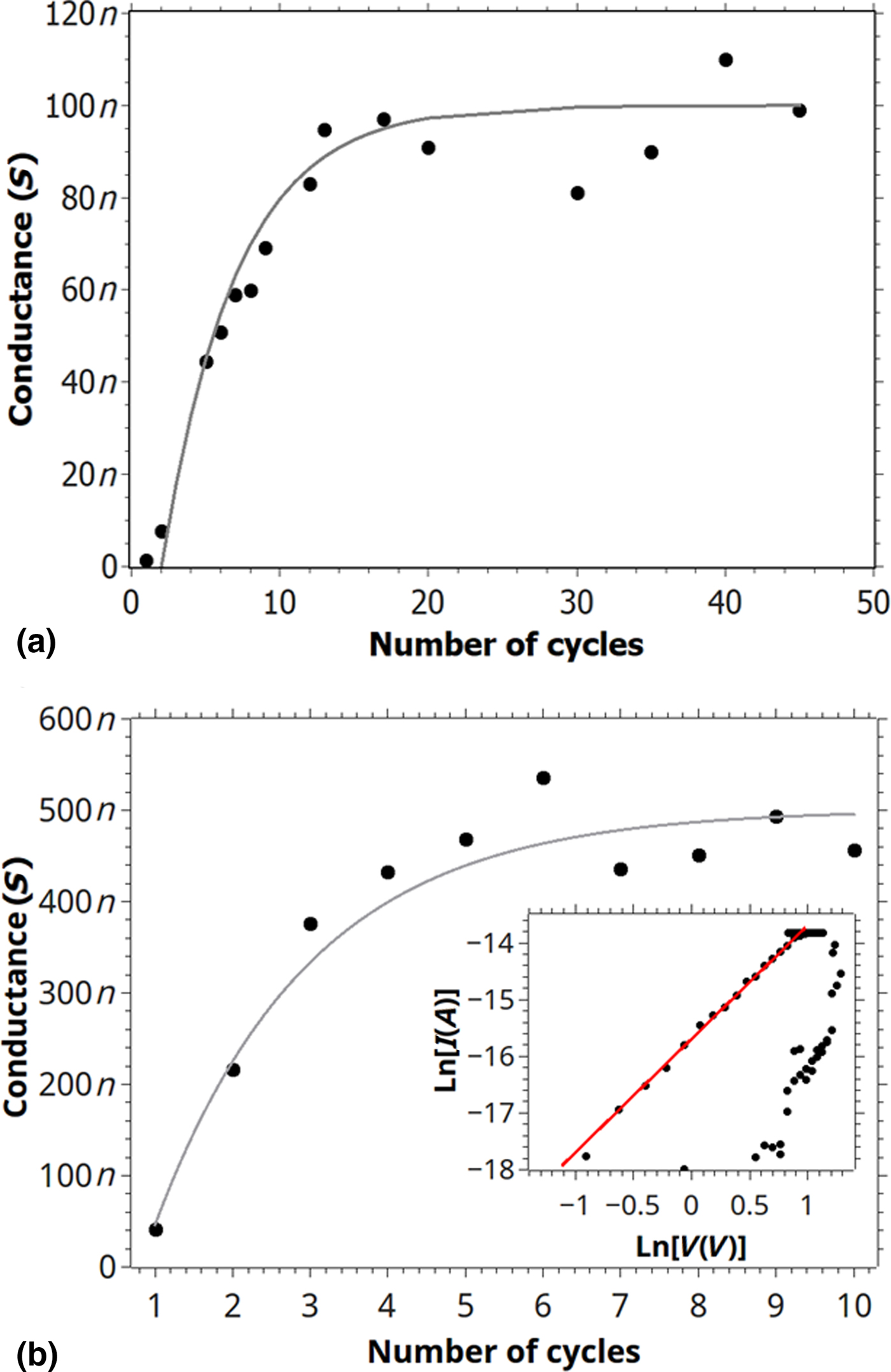
As more current is passed through the Ag-rich filaments in our devices, they become more conductive (as shown in Fig. 4). This is attributed to increased migration of Ag (from the contacts into the filament) brought about by repeated activity and/or by increased device current.[Reference Wang, Rao, Midya, Joshi, Jiang, Lin, Song, Asapu, Zhuo, Li, Wu, Xia and Joshua Yang13] The Rayleigh instability model also predicts that for a filament of fixed length, prolonged relaxation accompanies increased radius.[Reference Hsiung, Liao, Gan, Wu, Hwang, Chen and Tsai26] Our range of relaxation times (defined as time taken to fall to 50% of conductance in LRS) was 100–300 ms for filaments with lengths ranging from 200 to 700 nm. Measurements of relaxation times are plotted in Supplementary Fig. S4 and are comparable with many threshold switching devices incorporating Ag or Cu filaments.[Reference Wang, Rao, Midya, Joshi, Jiang, Lin, Song, Asapu, Zhuo, Li, Wu, Xia and Joshua Yang13] Other authors have shown that metallic filaments undergoing Rayleigh instability exhibit a linear relationship between the fourth power of their radius and their relaxation time.[Reference Zhao, Xu, Wang, Zhang, Ma and Liu27] Our data seem to follow this relationship (see Fig. S4). This is surprising given the barrier-limited transport shown in Fig. 2(c), which would suggest that the filaments are far from metallic.
Conductance of the filament (determined at half the current limit) in the LRS versus number of cycles with current limits of (a) 100 nA and (b) 1.00 µA imposed. The gray curves follow a model equation for saturation in biologic synapses (see main text). Inset in (b) shows that after the sixth sweep, transport in the LRS is consistent with space charge-limited conduction.

Figure 4 shows the evolution of the conductance of a device with a 700 nm filament with repeated I–V sweeps. Current limits of 100 nA [Fig. 4(a)] and 1 µA [Fig. 4(b)] were imposed and the conductance was measured at half the current limit in the LRS. Both plots are characterized by an initial increase in conductance then saturation. This behavior, routinely observed in biologic synapses, is critical for memory and learning. Its emulation by inorganic memristive devices has been reported by numerous authors.[Reference Zhu, Du, Jeong and Lu28] With the lower current limit imposed, the conductance is highly stochastic [Fig. 4(a)] consistent with a filament that is unstable on a timescale equivalent to one sweep. Nevertheless, saturation is evident and reasonable agreement is achieved between the experimental data and the gray curve in the plot. This curve follows G = G 0 + G sat(1− Ae−n/B) where G is the device conductance, G 0 is the conductance in the unformed (pristine) state, G sat is the saturation conductance, n is the sweep number, and constants A = 1.5 and B = 5. After the forming process, G 0 represents the comparatively small parallel conductance between the electrodes through the unmodified a-ZTO. Similar phenomenologic equations have been used to describe activity-dependent biologic synaptic efficacy[Reference Markram, Pikus, Gupta and Tsodyks29] and conductivity in inorganic memristors.[Reference La Barbera, Vincent, Vuillaume, Querlioz and Alibart30] Allowing a greater current through the device increases the saturation current and reduces the scatter in the conductance data [Fig. 4(b)]. Once again, the saturation behavior follows the model previously used to describe synaptic behavior with A = 1.5 and B = 2. The inset in Fig. 4(b) shows the LRS I–V characteristic during the sixth sweep. In contrast to the LRS I–V characteristics with the lower current limit imposed, a single current-limiting mechanism describes this I–V relationship. The square law dependence shown in the inset is consistent with space charge-limited conduction resulting from carrier injection into an insulating material. The emergence of this characteristic implies that at higher compliance, the junctions/interface layers at the electrodes are no longer the strongest influence on transport. When the higher current limit is imposed, the higher saturation conductance observed is the result of a more substantial filament (with larger radius). We suggest that the Ag/a-ZTO junctions are effectively “shorted out” by this more substantial filament.
The structure of the memristor reported here was chosen to facilitate microscopy following operation without additional sample preparation. Achieving the highest on:off resistance ratio, longest retention times and greatest stability were not aims of the study. The resistive switching endurance of these devices (shown in Fig. S5) is however promising and further experiments with encapsulated devices are planned. All devices tested exhibited synaptic plasticity and conduction saturation, both of which are widely acknowledged to be crucial in biologic memory. Aside from this aspect of their behavior, their fast relaxation and the significant LRS:HRS ratio show that there is potential for devices like these to serve as threshold switching selectors. These enable selective programming of individual memristors within arrays.[Reference Wang, Rao, Midya, Joshi, Jiang, Lin, Song, Asapu, Zhuo, Li, Wu, Xia and Joshua Yang13]
Conclusion
Planar Ag electrodes supported on a-ZTO with differing sub-micrometer separations have exhibited volatile-resistive switching and activity-dependent conductance after the formation of Ag-rich nanoscale filaments. Whilst Ag filaments have been reported to form in a long list of materials, we have not found a-ZTO included in this list, despite the effects of Ag migration being observed in Ag-gated a-ZTO transistors. Current–voltage measurements performed on the Ag/a-ZTO memristors showed that in the pristine state, the Pt/Ag contacts formed back-to-back Schottky contacts to the underlying a-ZTO. In the HRS state, current transport was consistent with Schottky emission. In the LRS, the filament exhibited transport behavior and threshold voltage that depended both on activity and on the current limit imposed. The filament was subject to Rayleigh instability and the LRS relaxation time was shown to increase when more current was passed through the device and the effective radius of the filament increased. Saturation of the device conductance after repeated I–V sweeps resembled biologic synaptic behavior. This work highlights the potential for transparent neuromorphic circuits combining a-ZTO-based TFTs and a-ZTO-based memristors.
Supplementary material
The supplementary material for this article can be found at https://doi.org/10.1557/mrc.2018.156.
Acknowledgments
The authors acknowledge support from the RMIT microscopy and microanalysis facility (RMMF), a linked laboratory of the Australian microscopy and microanalysis research facility. H.N. Tran and J.G. Partridge would also like to thank M.W. Allen at the University of Canterbury (New Zealand) for useful discussions.