Introduction
Electron energy-loss spectroscopy (EELS) in the transmission electron microscope has become an invaluable tool for unraveling the chemical compositions and structures of materials, enabling imaging of individual atoms and their bonding states with unprecedented resolutions.Reference Muller, Kourkoutis, Murfitt, Song, Hwang, Silcox, Dellby and Krivanek1,Reference Colliex2 The low-energy (“low-loss,” 0–50 eV) region of the EEL spectrum yields electronic information in the form of valence intraband and interband transitions, as well as plasmon excitations, rendering this part of the spectrum sensitive to changes in the overall electron density of the material. Conversely, the high-energy (“core-loss” >100 eV) region of the EEL spectrum is characterized by excitations of core-level electrons into well-defined higher-lying empty states and into the continuum, providing a technique suitable for studying the chemical state, local geometric structure, and nature of chemical bonding centered around the absorbing atom. When combined with the excellent spatial resolution of the transmission electron microscope, EELS constitutes a powerful technique for the electronic characterization of nanoscale materials.
However, if one wishes to study dynamical processes, the temporal resolution has been typically limited by the acquisition time of the detector (∼30 ms). Only recently, ultrafast EELS with temporal resolutions ranging from femtoseconds (fs) to nanoseconds (ns) has been demonstrated and applied to study laser-induced pre-ablation dynamicsReference Carbone, Kwon and Zewail3 and bandgap renormalizationReference van der Veen, Penfold and Zewail4 in graphite thin films, electron–phonon coupling and structural dynamics in multiwalled carbon nanotubes,Reference Vanacore, van der Veen and Zewail5 imaging of evanescent waves surrounding carbon nanotubes,Reference Barwick, Flannigan and Zewail6 plasmonic nanostructures,Reference Yurtsever, van der Veen and Zewail7–Reference Liu, Baskin and Zewail9 biological structures,Reference Flannigan, Barwick and Zewail10,Reference Kaplan, Yoo, Tang, Karam, Liao, Majumdar, Baltimore, Jensen and Zewail11 and photo-induced charge-transfer and phase transitions in transition-metal oxides.Reference Piazza, Ma, Yang, Mann, Zhu, Li and Carbone12,Reference Su, Baskin, Zhou, Thomas and Zewail13
This article discusses some of the latest results, prospects for applications, and new methods in ultrafast EELS at the nanometer scale. Refer to References Reference Flannigan and Zewail14–Reference LaGrange, Reed and Masiel17 for a detailed discussion of ultrafast and dynamic electron microscopy and References Reference Yalunin, Schröder and Ropers18–Reference Park, Lin and Zewail20 for a deeper theoretical understanding of inelastic electron–photon interactions.
Ultrafast core-level electron spectroscopy
Apart from relativistic effects in the former,Reference Jouffrey, Schattschneider and Hebert21 electron energy-loss and x-ray absorption core-level spectra are essentially equivalent and provide analogous information. Energy losses between 100 and 1500 eV are routinely accessible in transmission electron microscopy-EELS (TEM), which (partly) overlaps with the soft x-ray region. Ultrafast x-ray and extreme ultraviolet spectroscopies have experienced tremendous progress in recent years.Reference Chergui22–Reference Schultz and Vrakking24 Picosecond-resolved x-ray absorption spectroscopy implemented at synchrotron facilities has enabled the characterization of the excited state structure and dynamics of a wide variety of chemical systems. More recently, the advent of x-ray free-electron lasers has introduced a paradigm shift in terms of the temporal resolution of x-ray spectroscopies into the femtosecond regime. Importantly, due to the rather low interaction cross section of x-rays with matter, in situ studies of nanoscale objects such as thin films and individual nanoparticles are challenging, especially for materials containing low-Z (Z is atomic number) elements such as organic crystals, polymers, and biological molecules. This can be overcome by ultrafast EELS, which combines, in a tabletop apparatus, high spatial resolution and sensitivity to characterize individual nanostructures with the ultrashort temporal resolution and energy resolutions needed to address chemical dynamics immediately following laser excitation.
The feasibility of femtosecond- and nanosecond-resolved core-level EELS has recently been demonstrated by the study of photo-induced structural dynamics in graphite thin filmsReference van der Veen, Penfold and Zewail4 and charge-transfer dynamics in iron oxide photocatalysts.Reference Su, Baskin, Zhou, Thomas and Zewail13 These experiments revealed that core-level EELS is especially sensitive to chemical bonding properties (e.g., structure, symmetry, spin, and charge) in the close vicinity of the absorbing atom. Figure 1 shows experimental and simulated static and transient energy-loss near-edge spectra (ELNES) at the carbon K-edge (∼280 eV) after laser excitation at 532 nm. The transient core-loss spectra, in combination with ab initio molecular dynamics simulations, reveal the elongation of the carbon–carbon bonds, even though the overall behavior is a thermal contraction of the crystal lattice. A prompt energy-gap shrinkage is observed on the picosecond time scale (Figure 1c), which is caused by local bond length elongation and the direct renormalization of band energies due to temperature-dependent electron–phonon interactions. In femtosecond-resolved core-level EELS, caution is warranted in interpreting the dynamics between t = –1 ps and +1 ps, where the inelastic photon–electron (photon-induced near-field electron microscopy [PINEM], vide infra) effect significantly broadens the spectrum, as shown in Figure 1d. While in some cases careful deconvolution methods are needed to eliminate these features,Reference Su, Baskin, Zhou, Thomas and Zewail13 other experiments may exploit this technique to reveal material-dependent dynamics of plasmonic fields (e.g., due to photo-induced metallicity or electron–hole-pair dynamics).Reference Carbone25
(a) Nanosecond-resolved core-level electron energy near-edge spectrum (ELNES) at the carbon K-edge before photoexcitation (<t 0, black, right axis) and transient difference spectrum after laser excitation (Δt = 20 ns, red, left axis). The ELNES is characterized by out-of-plane π*(p z) and in-plane σ*(sp 2) resonances. Pronounced features across the whole spectrum indicate significant structural changes in the graphite thin film after photoexcitation. (b) Theoretical static (black, right axis, room temperature) and transient (gray, left axis, 900 K spectrum minus room-temperature spectrum) ELNES based on molecular dynamics simulations. A semi-quantitative agreement is achieved between the theoretical (b) and experimental (a) transient spectra. (c) The photon-induced near-field electron microscopy effect in core-level electron energy-loss spectroscopy, in which electron–photon interaction causes a broadening of the spectrum around t = 0. The color bar denotes difference intensity (a.u.). (d) Transient ELNES at Δt = 20 ± 10 ps after laser excitation.Reference van der Veen, Penfold and Zewail4 Note: t, time; t 0, time zero (temporal overlap of laser and electron pulses).

One of the challenges of ultrafast core-level EELS is that the cross section for inelastic scattering decays with a power-law energy dependence according to AE –r, with r = 2–5, A = constant, and E = energy.Reference Egerton26 Therefore, deep core-level edges (>100 eV) are considerably more challenging to measure than shallow core levelsReference Piazza, Ma, Yang, Mann, Zhu, Li and Carbone12 and low-loss plasmon excitations (0–100 eV).Reference Carbone, Kwon and Zewail3 In order to overcome these challenges and enhance the sensitivity necessary to measure such weak time-resolved signals at deep core-level ionization edges, careful data acquisition strategies (e.g., energy-drift correction), efficient detection schemes (e.g., direct electron detectionReference Hart, Lang, Leff, Longo, Trevor, Twesten and Taheri27), and new instrument developmentsReference van Rens, Verhoeven, Franssen, Lassise, Stragier, Kieft, Mutsaers and Luiten28–Reference Zhou, Williams and Ruan30 are necessary and already underway.
Compared to ultrafast optical transient spectroscopy, which mainly probes the delocalized/hybridized valence orbitals, or ultrafast electron diffraction, which tracks the overall structural changes of the material, the element specificity and simultaneous local electronic and structural sensitivity of ultrafast core-level EELS opens the door for a plethora of studies on the L-edges of transition-metal oxides that are of current interest for microelectronics, spintronics, photocatalytic water splitting, biosensing, and solar-energy conversion. Of particular importance are future studies of hole dynamics, which have remained largely unrevealed using conventional optical-probing techniques, as well as dependences of the electron–hole dissociation, trapping, and recombination time scales on the nanoparticle size, shape, and defect structure in prevalent photocatalysts.
Ultrafast low-loss electron spectroscopy with meV resolution
To characterize and manipulate many-body excitations in the low-energy spectral range of strongly correlated solids, one needs to simultaneously combine meV-spectral, nanometer-spatial, and femtosecond-temporal resolutions. Energy-filtered TEM of phonons and plasmons in nanostructures yields subnanometerReference Nellist and Pennycook31 and 10 s meV space/energy resolutionReference Rossouw and Botton32–Reference Lagos, Truegler, Hohenester and Batson34 under static conditions. To achieve a combined nm-fs-meV resolution, a laser-assisted ultrafast TEM method, where energy resolution is not determined by the electron beam and spectrometer energy spreading, but solely by the laser pulse linewidth, has been proposed.Reference Pomarico, Madan, Berruto, Vanacore, Wang, Kaminer, García de Abajo and Carbone35 In particular, spectral profiles of plasmonic resonances (PRs) with 20 meV resolution have been retrieved by performing PINEMReference Barwick, Flannigan and Zewail6,Reference Piazza, Lummen, Quiñonez, Murooka, Reed, Barwick and Carbone8,Reference Park, Lin and Zewail20,Reference Lummen, Lamb, Berruto, LaGrange, Dal Negro, García de Abajo, McGrouther, Barwick and Carbone36 with infrared (IR) tunable laser excitation combined with quantitative analysis of the obtained energy-filtered images. In PINEM, the near field that surrounds the interface or nanostructure facilitates the direct coupling of the imaging electrons with photons in the laser excitation pulse. The electrons (with energies typically on the order of 200 keV) absorb/emit integer numbers of photons, which can then be used to directly visualize the scattered evanescent field surrounding the nanostructure.Reference Park, Lin and Zewail20
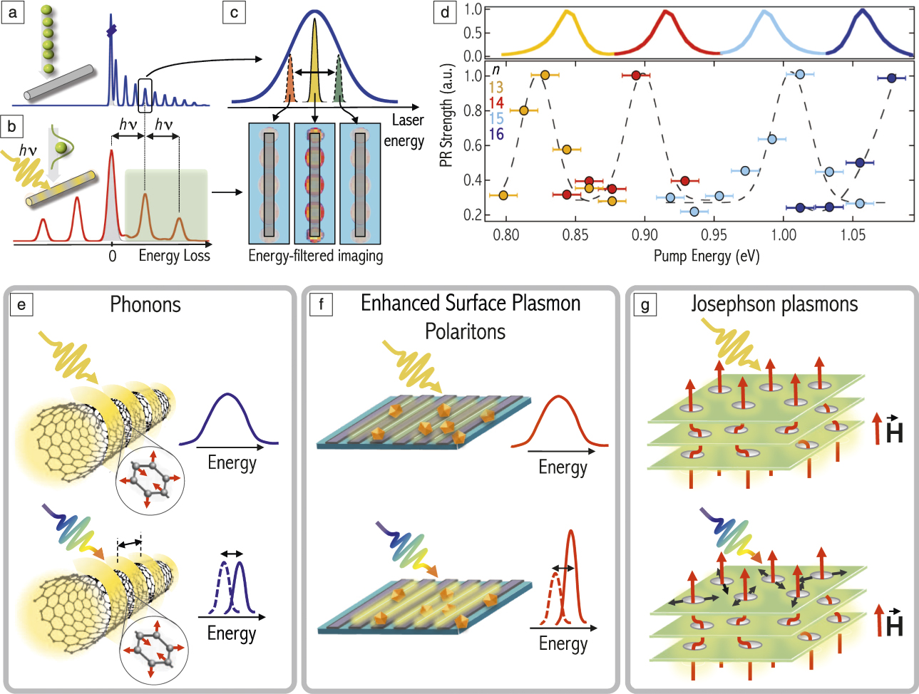
When electrons traverse the proximity of a nanostructure, the transient electric field associated with the electrons excites PRs, manifesting themselves as features in an energy-loss spectrum (Figure 2a). In ultrafast TEM, to reduce space-charge effects, the intensity of the electron pulses is strongly attenuated. Under these conditions, the energy bandwidth of the pulses is broadened to the eV level, limiting the investigation of features at smaller energy scales. By illuminating the nanostructure with an optical pulse at a resonant energy, a specific PR can be excited and multiples of the PR energy can be exchanged with the imaging electron beamReference Barwick, Flannigan and Zewail6,Reference Park, Lin and Zewail20 (Figure 2b). By scanning the laser wavelength across the PRs and mapping their spatial profile after filtering all inelastically scattered electrons (Figure 2c), one can resolve the modes with an energy resolution only limited by the laser linewidth, and not by the electron-beam energy bandwidth. The spectrum of PRs in an 8-μm-long Ag nanowire has been measured over the energy range between 800 and 1080 meV by using a modified microscope operated at 200 kVReference Piazza, Masiel, LaGrange, Reed, Barwick and Carbone37 in combination with an optical parametric amplifier in the near-IR working at 300 kHz repetition rate.Reference Pomarico, Madan, Berruto, Vanacore, Wang, Kaminer, García de Abajo and Carbone35 In Figure 2d, we show the measured spectra for n = 13–16 modes, which are in good agreement with simulations based upon boundary-element-method calculations of the optical field.Reference García de Abajo and Howie38,Reference García de Abajo, Barwick and Carbone39
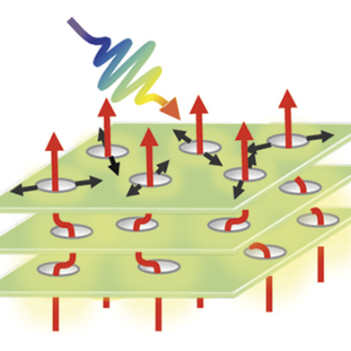
(a) Electron energy-loss (EEL) spectrum of plasmonic resonances (PRs) excited in a nanowire by passing electrons. (b) EEL spectrum upon photoexcitation by light pulses of energy hν of a specific plasmonic mode, which exchanges its characteristic energy several times with the electrons. (c) The laser excitation wavelength is scanned and the PR profile retrieved via a quantitative analysis of the energy-filtered images. (d) PR strength for modes n = 13–16 obtained by integrating the Fourier transforms of the parallel-to-the-wire spatial profiles of the PRs at specific periodicities and by scanning the laser energy between 0.8 and 1.08 eV (simulations on top). (e–g) Some phenomena that are inaccessible with standard ultrafast energy-filtered transmission electron microscopy (top in each panel), but approachable with the laser-assisted method (bottom in each panel). (e) Real-time spatial and spectral changes of the PR features of a carbon nanotube upon excitation of its infrared active phonons; (f) enhancement and spectral shift induced by nanostructures on the surface plasmon polaritons excited on a metallic grating; (g) spatial changes in real time of the vortex lattice in a layered superconductor upon excitation of a Josephson plasma mode.Reference Pomarico, Madan, Berruto, Vanacore, Wang, Kaminer, García de Abajo and Carbone35 Note: h, Planck’s constant; ν, frequency; H, magnetic field.

This method is a valuable tool for providing full dynamical characterization and control of low energy excitations, such as IR-active phonons, without relying on the energy broadening of the incident electron beam. The central frequency and the resolution used to image a specific mode are solely determined by the light-excitation properties. Optical sources of high monochromaticity and controlled temporal profile are readily available at energies covering a wide spectral range and can provide a broader parameter space compared with state-of-the-art electron optics. If one partially sacrifices time resolution, ultrahigh-resolution experiments (even below 1 meV) can be conceived by relying on the intrinsic linewidth of laser sources or spectral shaping techniques.
New fundamental aspects of coupling between different collective excitations, such as phonons and plasmonic fields in a nanostructure, could emerge via this laser-assisted method. For instance, by exciting the IR active phonons in carbon nanotubesReference Kim, Liu, Furtado, Chen, Saito, Jiang, Dresselhaus and Eklund40 optically or by impulsive stimulated Raman scattering, one could investigate the effects on the spatial profile and the spectral changes of the PRs in real time (Figure 2e). Perspectives in chemistry and sensing include the possibility of tracking reaction trajectories and tailoring the chemical sensitivity of nanosensors using this technique.Reference Anker, Hall, Lyandres, Shah, Zhao and Van Duyne41 For example, the optical enhancement produced by coupling to plasmonsReference Wark, Lee, Qavi and Corn42,Reference Lv, Leong, Jiang, Kou, Dai, Lin, Liu and Si43 could be spatially and spectrally probed in a complete way (Figure 2f). In addition, new opportunities are offered for exploring exotic properties of quantum solids at low energies, such as longitudinal Josephson plasmons (JPs) in layered superconductors,Reference Shibata and Yamada44 arising from the tunneling of Cooper pairs between the superconducting planes. By combining tunable optical excitation with cryo-Lorentz microscopy,Reference Park, Baskin and Zewail45 one can visualize the dynamical changes of the vortex lattice induced by the external magnetic field upon excitation of a JP (Figure 2g).
Single-shot EELS to probe irreversible light-induced phenomena
The stroboscopic laser-pump electron-probe method achieves ∼100 fs and sub-eV time and energy resolutions, respectively, by integrating electron counts from many pump-probe cycles in order to obtain sufficient signal in the EEL spectrum. In this scheme, repetitive measurements are made on the same region of a specimen such that observable processes are limited to only highly repeatable, reversible ones, for which the photoexcited specimen must fully return to its original state before successive pump pulses arrive. If a sample undergoes an irreversible process, which is more common in, for example, phase transitions or chemical reactions, the approach should be based on a single laser excitation “shot” and a sequence of subsequent electron pulses that captures the course of the unique irreversible process.Reference LaGrange, Reed and Masiel17 The single-shot approach requires short electron probe pulses that are intense enough to generate a spectrum with sufficient signal-to-noise ratio. Dense electron pulses, however, are subject to significant Coulomb repulsion, which not only limits the formation and propagation of the pulses, but also disperses the energy of electrons; pulsed electrons under space-charge effects tend to broaden in space, time, and energy.Reference Siwick, Dwyer, Jordan and Miller46
In order to realize EELS of irreversible processes, two key challenges need to be overcome. First, to satisfy the two extreme conditions of maximized electron counts and minimized energy spread, one needs to optimize the initial state of the photoemitted electron pulse. This can be done by changing the physical shape of the cathode, gun geometry, extraction field, pulse duration, irradiation region, and UV laser fluence. The replacement of a sharp tip with a flat cathode with large emission area can increase the number of electrons by a few orders of magnitude while preserving similar space-charge effects, but compromising spatial coherence.Reference Lee, Kim, Kim and Kwon47 The control of the gap between the cathode surface and the exit aperture of a Wehnelt electrode, which focuses the electron beam after emission, and the electric field around the aperture, can be used to find a configuration for which the number of electrons and their energy spread are optimized.Reference Kieft, Schliep, Suri and Flannigan48–Reference Ji, Piazza, Cao, Park, Reed, Masiel and Weissenrieder50 The temporal elongation of the pulsed electrons up to a microsecond regime can further increase the number of electrons in a single pulse in the space-charge quasi-free regime by another order of magnitude, reaching a total current of milliamperes, which is equivalent to the steady-state current of thermionic electron sources.
The second technical challenge comprises the dispersion and deflection of a sequence of electron pulses onto different regions of the camera in order to make a “movie” of the ensuing events after laser excitation. Bostanjoglo et al.Reference Dömer and Bostanjoglo51 pioneered this “movie-mode” approach, and it was further developed by researchers at Lawrence Livermore National Laboratory.Reference LaGrange, Reed and Masiel17,Reference LaGrange, Reed, Santala, McKeown, Kulovits, Wiezorek, Nikolova, Rosei, Siwick and Campbell52 This approach is based on inserting a fast, electrostatic deflector into the transmission electron microscope imaging system after the specimen. An electronic timing system switches the voltage of the deflector in the dead time between the incident electron pulses that are generated by a powerful high repetition rate laser system. This technique has been successfully applied to capture images and diffractograms of irreversible processes, such as ultrafast meltingReference LaGrange, Campbell, Reed, Taheri, Pesavento, Kim and Browning53 and reaction dynamics in nanolaminates,Reference LaGrange, Reed and Masiel17,Reference Kim, LaGrange, Reed, Taheri, Armstrong, King, Browning and Campbell54 with temporal resolutions far exceeding the video-rate millisecond resolution. Its future extension for single-shot EELS studies will merely involve the adaptation of the deflector system to project EEL spectra along the camera direction perpendicular to the dispersion direction of the imaging system. Since EEL spectra are typically only projected onto a fraction of the camera, no compromise in energy resolution is required (in contrast to movie-mode imaging or diffraction that needs to sacrifice resolution).
The methodological concept of single-shot EELS is schematically presented in Figure 3. The foreseen characteristics comprise exposure times as short as a few microseconds, time series of up to a dozen pulses with microsecond relative temporal spacing, and energy spreads of a few eV. An increase in energy resolution may be obtained by deconvoluting the inherent energy spread of the electron optics system and the point spread function of the detector by utilizing the “zero-loss” peak (composed of unscattered and elastically scattered electrons) measured in the same experiment.Reference Wang, Egerton and Malac55 While the capabilities of single-shot EELS may appear inferior in terms of temporal and energy resolution compared to the stroboscopic time-resolved EELS techniques, its much wider applicability for studying prevalent irreversible processes, such as thermally and photo-induced phase transformations (including melting) and reactions in chemistry and materials science, encourages its emergence in the near future.Reference Yoo, Kwon, Liu, Tang and Zewail56–Reference Picher, Bücker, Lagrange and Banhart59
The principle of single-shot electron energy-loss spectroscopy (EELS). Structural and electronic dynamics in the specimen are initiated by a single laser pump pulse, after which an electron-probe pulse train captures the light- (or temperature-jump)-induced processes. The time interval between electron pulses is variable from nanoseconds to microseconds, and the whole pulse train is delayed by time interval, Δt, with respect to the laser excitation pulse. A fast, electrostatic deflector in the post-specimen column is used to deflect the sequence of electron pulses along the axis perpendicular to the direction of energy dispersion in the EEL spectrometer. An “EELS cube” (energy E, time t, electron counts) is recorded in a single acquisition enabling the study of irreversible processes (inset on the right). Note: CCD, charge-coupled device.

Conclusions
Ultrafast TEM has emerged as a powerful tool for understanding the evolution of atomic and electronic rearrangements under nonequilibrium conditions in organic, inorganic, and biological materials. Imaging and diffraction alone are incapable of capturing fine modulations in chemical composition and bonding, charge-transfer dynamics, or spin-state changes that often accompany structural reorganizations in materials triggered by external stimuli. Ultrafast EELS therefore complements the crucial fourth dimension (energy) in the dynamic multidimensional visualization of real materials, and transforms a TEM into a true “chemiscope,” capable of capturing element-specific snapshots of evolving (nano)structures (e.g., under light, pressure, chemical, or electrical bias), tracking and controlling collective excitations in strongly correlated materials, or mapping plasmonic fields at nanostructure interfaces. This article presented the state of the art and future perspective of a few particularly promising directions in ultrafast EELS, namely ultrafast core-level EELS for the study of transition-metal charge-carrier and spin-state dynamics in heterogeneous catalysis, ultrafast low-loss EELS with meV energy resolution for phonon and plasmon mapping, and single-shot EELS for studies of irreversible phenomena such as phase transitions. Future technological advances in electron sources, acquisition, and detection development are anticipated to enable studies with increased energy resolution and better sensitivity at higher energy losses, as well as new probing schemes for dynamic multimodal probing of the structure and functionality of a material.
Acknowledgments
E.P. and F.C. acknowledge support from the SNSF (P300P2_158473) and from the NCCR MUST. O.H.K. and Y.J.K. acknowledge support from the Institute for Basic Science (IBS-R020-D1) and NRF Korea funded by the Ministry of Science, ICT and Future Planning (MSIP) (2017R1A2B4010271). R.M.V. is grateful for startup funds provided by the Department of Chemistry at UIUC.

Enrico Pomarico is a research scientist at the École Polytechnique Fédérale de Lausanne (EPFL), Switzerland. He received his PhD degree in quantum optics from the University of Geneva, Switzerland, in 2011. He joined the Laboratory of Ultrafast Spectroscopy at EPFL and the Max Planck Institute for the Structure and Dynamics of Matter in Hamburg in 2015. He has studied spin–orbit and electron–phonon coupling effects at short time scales in molecular and solid systems. His current research focuses on combining ultrafast THz optics with transmission electron microscopy to investigate low-energy excitations in quantum solids. Pomarico can be reached by email at enrico.pomarico@epfl.ch.

Ye-Jin Kim is a doctoral candidate at Ulsan National Institute of Science and Technology, South Korea. She earned her MS degree in 2018 exploring chemical reaction dynamics using time-resolved spectroscopic methods. Her current research focuses on pushing the spatiotemporal resolution of ultrafast electron microscopy to the limit, and its application to the study of the ultrafast structural and electronic dynamics of matter at the nanoscale. Kim can be reached by email at gne1019@unist.ac.kr.

F. Javier García de Abajo is a professor at the Catalan Institution for Research and Advanced Studies and a group leader at the Institut de Ciències Fotòniques, Spain. He received his PhD degree from the University of the Basque Country, Spain, in 1993, completed postdoctoral research at Berkeley National Laboratory, and was a research professor at the Spanish Research Council. He is a Fellow of both the American Physical Society and The Optical Society. His current interests include surface science, electron microscopy and spectroscopy, nanophotonics, and plasmonics. García de Abajo can be reached by email at javier.garciadeabajo@nanophotonics.es.

Oh-Hoon Kwon has been an assistant professor in the Department of Chemistry at Ulsan National Institute of Science and Technology (UNIST), South Korea, since 2013. He received his BS degree in 1998 and his PhD degree in 2004, studying picosecond-resolved spectroscopy, both at Seoul National University, South Korea. During postdoctoral training and later as a senior scientist at the California Institute of Technology, he focused on developing the second-generation ultrafast electron microscope (UEM). At UNIST, he is building a high-spatiotemporal resolution UEM for the expansion of its scope to study dynamic phenomena of matter. Kwon can be reached by email at ohkwon@unist.ac.kr.

Fabrizio Carbone is a professor at the École Polytechnique Fédérale de Lausanne, Switzerland. He obtained his PhD degree in condensed-matter physics from the University of Geneva, Switzerland, in 2007. He then spent two years at the California Institute of Technology conducting ultrafast electron diffraction experiments on organic thin films. His current research focuses on ultrafast optical and electron-based techniques for the investigation of strongly correlated solids and nanostructures. Carbone can be reached by email at fabrizio.carbone@epfl.ch.

Renske van der Veen joined the faculty in the Department of Chemistry and the Frederick Seitz Materials Research Laboratory at the University of Illinois at Urbana-Champaign, as an assistant professor in 2015. She obtained her PhD degree in 2010 from the École Polytechnique Fédérale de Lausanne, Switzerland, in the field of ultrafast x-ray spectroscopy. She became a postdoctoral researcher at the California Institute of Technology, working on ultrafast electron microscopy and spectroscopy, after which she was a project group leader at the Max Planck Institute for Biophysical Chemistry, Germany, from 2013 to 2015. Her current research focuses on unraveling solar-energy conversion pathways using ultrafast x-ray and electron-based tools. Van der Veen can be reached by email at renske@illinois.edu.