Introduction
The first developments on stretchable circuits were reported in the early 2000s in a number of U.S.-based research institutes, including Lawrence Livermore National Laboratory,Reference Maghribi, Hamilton, Polla, Rose, Wilson and Krulevitch1 Princeton University,Reference Lacour, Wagner, Huang and Suo2 and Johns Hopkins University.Reference Gray, Tien and Chen3 All of these technologies used thin-film metallization (evaporation or sputtering) on an elastic polydimethylsiloxane (PDMS) substrate. Since those early days, many more interesting technology developments have been reported worldwide, exploring the use of a wide variety of materials such as composite and liquid conductors,Reference Kim, Son and Ziaie4 ultrathin bendable silicon,Reference Khang, Jiang, Huang and Rogers5 and perforated polyimide sheets.Reference Someya, Kato, Sekitani, Iba, Noguchi, Murase, Kawaguchi and Sakurai6 In the current article, the focus is on a technology that makes use of conventional rigid and flexible printed circuit board (PCB) processing equipment. This reasoned choice was made taking a potential future transfer of the technology to an industrial production environment, including compatibility with existing conventional electronic circuit fabrication equipment, in mind.
Therefore, the stretchable circuit technology, which will be described later, shows some similarities with conventional PCB fabrication and assembly technologies.Reference Bossuyt, Guenther, Loher, Seckel, Sterken and de Vries7, Reference Fjelstad and Vanfleteren8 Like these technologies, it involves the use of:
• Standard copper conductor material as interconnections
• Lithography and wet etching technology for the patterning of copper conductors
• Conventionally packaged off-the-shelf electronic components and sensors, providing the capability to realize circuits with a high degree of complexity and functionality
• Standard solder assembly technology for mounting components on the copper tracks of the stretchable PCB.
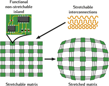
Since normal off-the-shelf components are rigid, it is clear that the areas in the circuit where the components are present cannot deform. The overall concept of a stretchable circuit is illustrated in Figure 1.Reference Fjelstad and Vanfleteren8, Reference Bossuyt, Vervust, Axisa and Vanfleteren9 The circuit comprises a number of rigid (or moderately flexible in some cases) component islands, where each island holds a single component or a limited number of components. The total area of each island is small and acceptable for the application in which the stretchable circuit is to be used. The interconnection between the components on a single island can be formed using the same copper conductor foil that provides the stretchable interconnects. Alternatively, these components can first be mounted on a separate (small) standard PCB or FCB interposer board, acting as an interface between components and stretchable interconnects. The interposer board is subsequently assembled on the large-area stretchable circuit. A proper design and technological implementation of the transition between the rigid component islands and the stretchable meander copper conductors (see the section on Mechanical modeling and design) is extremely important for obtaining a desired level of mechanical reliability (i.e., under cyclic stretching) of the circuit. As a general rule, a gradual transition from rigid to flexible to stretchable is necessary to obtain a mechanically reliable circuit.
Stretchable circuit concept:Reference Fjelstad and Vanfleteren8, Reference Bossuyt, Vervust, Axisa and Vanfleteren9 Functional non-stretchable islands, including electronic components, are interconnected with electrically conductive stretchable interconnects forming a conformable matrix.

In order to build PCB-style stretchable circuits, two main approaches are followedReference Bossuyt, Guenther, Loher, Seckel, Sterken and de Vries7 in currently ongoing research:
• The first approach is the one where the starting material for the circuit is a stretchable carrier, laminated on top of a copper conductor sheet. The electrical circuit is then fabricated by first patterning and wet etching the copper, followed by assembly of the components. This kind of process has exactly the same sequence of steps as normally found in PCB fabrication, and therefore intuitively is very close to normal rigid or flexible printed circuit manufacturing and assembly. However, the presence throughout the process of the stretchable carrier, which often has limited resistance to chemicals or limited operating temperature range, makes careful processing necessary. For example, low melting temperature solders such as eutectic SnBi (melting temperature 139ºC) or conductive adhesives must be used to assemble the components. The presence of the stretchable carrier, for which currently mainly polyurethane is used, does not allow the use of conventional lead-free SnAgCu solders, which require process temperatures of typically 250ºC. Despite these limitations, this technology, which is called stretchable copper board (SCB), is successfully being developed, and a number of attractive functional demonstrators have been presented.Reference Ostmann, Loher, Seckel, Bottcher and Reichl10
• In the second approach,Reference Fjelstad and Vanfleteren8 the circuit is first produced on a temporary carrier, including the steps of Cu pattern definition and wet etching, followed by component assembly. In the second phase, the stretchable carrier material is applied (e.g., by liquid injection molding [LIM]), and the temporary carrier is removed. This process is intuitively less close to conventional PCB processing, compared to the first approach, but has the advantage that all high temperature steps and harsh wet chemistry steps can be executed in the absence of the stretchable carrier.Reference Bossuyt, Guenther, Loher, Seckel, Sterken and de Vries7, Reference Fjelstad and Vanfleteren8 This article will focus on different aspects of this latter technology, which is called stretchable molded interconnect (SMI), as most of mechanical modeling and reliability assessment data are available for this technology.
In subsequent sections, we describe ongoing activities on mechanical modeling, technology development, reliability assessment, and applications.
Mechanical modeling and design
For the fabrication of PCB-based stretch circuits, Cu is the obvious choice for the electrical interconnection material. This conductor is widely used in PCB manufacturing because of its combination of high electrical conductivity and relatively low cost. Given the fact that the ultimate strain to fracture of bulk Cu is limited to a few percentage, it is clear that in stretchable circuits, the Cu conductors cannot be applied as straight lines, as in rigid or flexible printed circuits.Reference Gonzalez, Vandevelde, Christiaens, Hsu, Iker, Bossuyt, van der Sluis and Timmermans11 The conductors should be given some kind of spring shape, allowing reversible deformation from a compact/contracted state under zero mechanical stress to an elongated state under tensile stress. This implies the introduction of a kind of periodic curling or zigzagging of the conductors. This curling can be implemented, either in the plane of the circuit, which could be called a meander type of interconnection, or out of the circuit plane, which then could be called an accordion type of interconnection.Reference Maghribi, Hamilton, Polla, Rose, Wilson and Krulevitch1, Reference Rogers12, Reference Song, Jiang, Choi, Khang, Huang and Rogers13 In this contribution, we have chosen to implement meander-type conductors because of their compatibility with normal PCB conductor patterning practices.
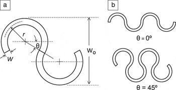
Much effort was subsequently spent on the proper design of the meanders. An aim of the design and modeling activities was to minimize stress and strain concentrations in the meander under deformation. Therefore, the stress has to be distributed as much as possible along the meander. It was shown that triangular and sinusoidal shaped meanders exhibit high stress concentrations at the top of the meander, resulting in early failures under repeated uniaxial stretch tests. The current meander shape of choice is the horseshoe shape,Reference Gonzalez, Axisa, Vanden Bulcke, Brosteaux, Vandevelde and Vanfleteren14, Reference Hsu, Gonzalez, Bossuyt, Axisa, Vanfleteren and De Wolf15 as shown in Figure 2. A horseshoe-shaped meander is a connection of circular segments and offers a good compromise between sufficient stress distribution along the meander on the one hand, and ease of design and circuit layout on the other. For minimal stress, the width (W) of the track should be as small as possible. This minimum W is determined mainly by technological constraints. In conventional PCB manufacturing, where the conductors are patterned by lithography and wet etching of a 17- or 35-μm-thick Cu sheet, conductor tracks with W = 100 μm provide circuits with sufficient process yield. Therefore, we have used W = 100 μm as a standard meander width. r and θ are design parameters. The values chosen for these parameters will depend on the application requirements (e.g., the maximum desired stretchability of the circuit). It is clear that for a certain r and W, an increasing θ will mean not only increasing maximum stretchability but also increasing overall width (W O) of the meander, and thus a decrease in the possible number of parallel running meanders per unit width of the total stretchable interconnect area. During the cycling elongation of the stretchable circuit, a permanent deformation or plastic strain is induced in the metal causing fatigue failure. Therefore, in order to improve the fatigue reliability of the stretchable interconnect, the plastic strain has to be minimized.
(a) Geometrical parameters of a horseshoe patterned stretchable interconnect; (b) horseshoe interconnections with different turning degrees (θ = 0° and 45°).Reference Gonzalez, Axisa, Vanden Bulcke, Brosteaux, Vandevelde and Vanfleteren14 Note: r, radius of curvature; W, track width; W O, overall width.

The ratio r/W determines the maximum plastic strain in the meander for a given deformation. In general, for deformations of 20% and less, the maximum plastic strain decreases with increasing r/W.Reference Gonzalez, Axisa, Vanden Bulcke, Brosteaux, Vandevelde and Vanfleteren14 However, high r/W ratios also mean meanders with high overall width, and thus a low density of parallel running meanders. A ratio of r/W = 10 normally offers a good compromise between low maximum plastic strain in the meander and high number of parallel running meanders per unit width of the stretchable interconnect area.
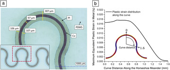
Further improvement of the mechanical reliability of the meanders is achieved by supplying the meanders with a flexible support. In the current state of the technology (see the next section), the support consists of a polyimide (PI) layer. PI materials with different elastic moduli, thicknesses, and patterned widths can be applied. Figure 3a shows a 100-μm-wide Cu meander, supported by a 300-μm-wide PI layer.Reference Fjelstad and Vanfleteren8, Reference Hsu, Gonzalez, Bossuyt, Vanfleteren and De Wolf16 Numerical modeling showed that the PI width is the main parameter, influencing (in fact reducing, compared to non-supported meanders) the maximum plastic strain in the Cu meander.Reference Hsu, Gonzalez, Bossuyt, Vanfleteren and De Wolf16, Reference Axisa, Bossuyt and Vanfleteren17 Supporting the meanders resulted in a significant improvement of the mechanical reliability, as discussed later in the reliability section. This can be explained by the redistribution of the plastic strain in the metal. Figure 3b shows the maximum plastic strain distribution along the curve length of a single meander horseshoe at 40% elongation.
(a) 100-μm-wide Cu horseshoe meander, supported by a 300-μm-wide polyimide layer; (b) plastic strain distribution along the supported meander at a uniaxial stretching of 40%.Reference Hsu, Gonzalez, Bossuyt, Axisa, Vanfleteren and De Wolf15 Note: PDMS, polydimethylsiloxane; PI, polyimide.

Finally, mechanical reliability tests have shown that under uniaxial stretching, the transition areas between the rigid or flexible component islands and the stretchable interconnections are even more sensitive to mechanical failure than the stretchable interconnects. There is no standard quantitative structural design rule or optimized design available for solving this reliability issue. A qualitative rule is that the transition from rigid over flexible to stretchable circuit parts should be as smooth as possible. Examples of how this can be realized are shown in the section on reliability.
Technology description
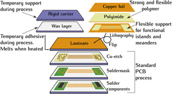
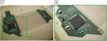
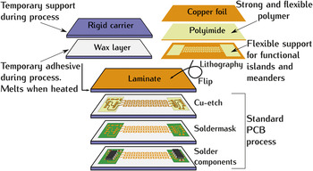
The first steps in the SMI process flow are shown in Figure 4.Reference Fjelstad and Vanfleteren8 A temporary rigid carrier (e.g., a standard PCB-class, fiberglass reinforced, epoxy laminate board) is covered with a temporary adhesive (e.g., wax) (Figure 4, top left). Separately (Figure 4, top right), a standard copper sheet (17 μm or 35 μm thick) with a patterned flexible support layer is fabricated. This flexible support layer can be a photo-definable spin-on PI, such as HD4110. The flexible PI layer, which is optional, serves as support material for the copper meanders and for the component islands. Supporting the meanders with a PI carrier has proven to greatly improve the mechanical reliability and operational lifetime of the copper meander circuits. The copper sheet with patterned support layer is subsequently laminated on the temporary carrier, using the wax as a lamination adhesive. After the lamination step, the patterned support layer is located between the temporary adhesive and the copper sheet. Next, the specially prepared laminate goes through a number of standard PCB manufacturing and assembly steps. Copper meanders, along with the standard design interconnections on the component islands, are patterned by photolithography and wet etching. A solder mask is locally applied by screen printing. If necessary, a contact pad finish is applied, and components are mounted using a conventional SnAgCu reflow solder process. At this point, the circuit can be tested and repaired, if required. At this stage of the process, no stretchable substrate materials have been used, which allows for the use of higher temperature solders. Figure 5 shows an SMI substrate after component assembly. The circuit is part of a respiration monitor developed in the frame of the STELLA project.18 The respiration monitor measures elongation through movements of the chest and the abdomen. This elongation is measured by two capacitive sensors.
Stretchable molded interconnect circuit fabrication: A stretchable circuit consisting of flexible islands and stretchable interconnects is fabricated by conventional printed circuit board (PCB) techniques on a temporary carrier. Adhesion between circuit and carrier is realized by using a temporary adhesive, which is removed during the succeeding molding steps.Reference Fjelstad and Vanfleteren8
Assembled stretchable molded interconnect circuit on a temporary carrier: (a) overview and (b) detail.Reference Fjelstad and Vanfleteren8 Device size is ∼5 × 8 cm2.

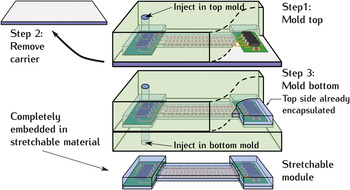
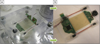
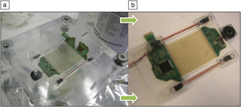
The second set of SMI process steps involves the application of the stretchable carrier material, giving the circuit its resilience (Figure 6).Reference Fjelstad and Vanfleteren8 In the first step, the top of the circuit is covered by a first layer of stretchable carrier material. Figure 6 shows the process variant, which is presently the method predominantly used at Ghent University (Belgium). The process involves a liquid injection molding (LIM) process, in which a top mold is placed over the circuit, a liquid two-component PDMS mixture is injected, and the mixture is subsequently cured at relatively low temperatures (ranging from room temperature to a maximum of 70°C for high-speed curing). Alternatives for the application of the stretchable carrier material by LIM include cover lamination and spraying. Besides PDMS, polyurethane (PU) or any polymer for which a liquid precursor or a thermoplastic variant is available can likely be applied. In the second step, the temporary adhesive is heated to the melting temperature, allowing for removal of the assembly from the temporary carrier. After cleaning (removal of the remaining adhesive from the assembly using an organic solvent or other suitable cleaner), the circuit is completely embedded by applying a second layer of stretchable material at the bottom (i.e., by the second LIM step). After the molds are removed, an embedded SMI stretchable circuit is the final product. Figure 7 shows the SMI respiration monitor circuit of Figure 5 during the LIM bottom molding step, as well as the final result after removal of the mold substrates. A variant of the SMI technology described earlier is one where the starting substrate is a commercially available flex laminate from which the component islands and copper meander circuits are defined by laser structuring and subsequent removal of the cut-out excess flex parts.Reference Axisa, Bossuyt and Vanfleteren17 Such a process, similar to that for the spin-on polyimide supported Cu conductors described previously, also yields copper meander circuits integrally supported by PI. Such meanders have very high mechanical reliability, but the step of removing the excess flex parts is difficult to achieve on an industrial scale.
Stretchable molded interconnect encapsulation procedure: The stretchable circuit adhering to the temporary carrier is partly encapsulated by injection molding the polymer on top of the circuit. After curing the polymer, the temporary carrier is removed, including the temporary adhesive. A second molding step takes place in order to fully encapsulate the device in a stretchable polymer.Reference Fjelstad and Vanfleteren8

Stretchable molded interconnect circuit (a) during and (b) after the liquid injection molding process.Reference Fjelstad and Vanfleteren8 Device size is ∼5 × 8 cm2.
Reliability assessment
Mechanical reliability is assessed by executing uniaxial stretching tests on samples that contain a number of parallel running meanders. Two types of tests are executed:
• One-time stretching until conductor rupture.
• Fatigue testing at different moderate elongations until conductor rupture.
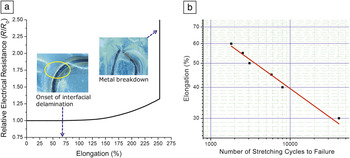
Figure 8a shows the results of an electromechanical measurement of a PI-enhanced stretchable interconnect sample during one-time stretching.Reference Hsu, Gonzalez, Bossuyt, Vanfleteren and De Wolf16 The electrical resistance was continuously recorded until metal rupture. The measured electrical resistance of the PI-enhanced stretchable interconnect is not constant but changes with elongation. Starting from 110% elongation, the electrical resistance gradually increases. This phenomenon can be explained by the fact that multiple micro-cracks initiate and propagate in the metal. This micro-crack propagation is retarded and held from complete metal rupture by the PI layer, while in the case of unsupported Cu meanders, an instant rupture of the Cu above a certain deformation threshold is observed.Reference Hsu, Gonzalez, Bossuyt, Vanfleteren and De Wolf16 The PI support gives the possibility to extend or “maximize” the ultimate elongation of the stretchable interconnect. With PI support, the ultimate elongation is 250%, which is two times the maximum magnitude of elongation shown in the case where no PI layer was used. It should be noted that the onset of interfacial delamination between the PI layer and the PDMS substrate is marked at 65% elongation, as shown in the inset of Figure 8a. Even though this delamination exists, the metal is still fully encapsulated and protected by the PI layer, which functions as a barrier against failure. It is clear that the PI layer provides an extra protection for the metal conductor.
(a) Electrical resistance of a polyimide (PI)-supported Cu meander during a one-time stretching experiment; (b) PI-supported meander lifetime as a function of elongation under cyclic stretching tests.Reference Hsu, Gonzalez, Bossuyt, Vanfleteren and De Wolf16 Note: R 0, initial electrical resistance; R, electrical resistance.

In Figure 8b, results are shown for cyclic stretching tests on PI supported meanders. The graph shows a power law fitting of the elongation versus the number of stretching cycles to failure. The experiments were performed with different levels of elongation, starting from 30% up to 60%. The strain rate was controlled at 1%/sec, and the electrical resistance was measured every five seconds. It was observed that the PI-enhanced stretchable interconnect withstands more than 40,000 stretching cycles at 30% elongation. Even for elongations up to 60%, the PI-enhanced stretchable interconnect can survive more than 1000 cycles. The lifetime improvement of the meanders strongly depends on the type and geometry of the supporting material. The results shown here were obtained for a double-sided Cu meander support consisting of a laminate type PI on one side and a spin-on PI on the other.Reference Axisa, Bossuyt and Vanfleteren17 This resulted in a 470 factor of improvement in the lifetime, compared to the unsupported meander case. More simple versions, such as the single-sided, spin-on PI-based technology, shown earlier, will result in an improvement with a factor 2 to 10.
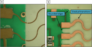
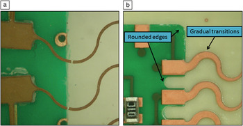
As mentioned previously, stretching tests on samples with embedded components have shown that design and fabrication technology of the transition areas between the individual components or component islands and the copper meanders greatly affect mechanical reliability and appear to be even more critical than the meanders themselves. As an example, Figure 9a shows a non-optimized sample after stretch testing.Reference Fjelstad and Vanfleteren8 Breaks in the interconnections are clearly visible, and they occur in the transition area at a much greater frequency than in the fully stretchable area. Figure 9b shows an optimized design, featuring gradual transitions in width of the copper and corresponding supporting PI, a design that reduces the local plastic strain in the copper, and the replacement of sharp-edged rectangular component island transitions with optimized structures (rounded edges). The combination of these two changes significantly mitigates the stress concentrations that were present in the original design.Reference Fjelstad and Vanfleteren8
(a) Non-optimized and (b) optimized design at a transition area between rigid/flexible and stretchable zones. Gradual transitions in width of the copper and corresponding supporting polyimide reduce the local plastic strain in the copper. Sharp edges need to be omitted.Reference Fjelstad and Vanfleteren8 Copper track width is ∼100 μm.
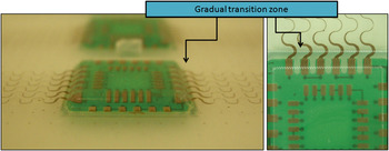
To further smooth the transition, the described design considerations in the plane of the circuit can be combined with reinforcement in the direction perpendicular to the substrate plane. A gradual transition in thickness of the encapsulant between thick regions (>1.0 mm) at the component islands and thin regions (<1.0 mm) situated at the position of the stretchable interconnects avoids local stress concentrations in the transition area (Figure 10).Reference Fjelstad and Vanfleteren8 This improvement helps to distribute the stress over a wider region, enhancing the lifetime of the interconnections and transition zones.
Gradual transition in encapsulant thickness between rigid/flexible and stretchable zones avoids local stress concentrations in the transition area.Reference Fjelstad and Vanfleteren8

Applications
There are a number of applications where the use of conventional flat rigid assembled PCBs becomes problematic because there is a need to comfortably integrate the circuit on a non-flat surface. Often, wearable and implantable circuits (such as those used for biomedical applications, sports and leisure, safety, and smart textiles) require non-flat assemblies because the circuit must follow the irregular shapes of the part onto or into where the circuit is integrated.Reference Axisa, Jourand, Lippens, Rymarczyk-Machal, De Smet, Schacht, Vanfleteren, Puers and Cornelissen19, Reference Wu, Liu, Song, Huang, Hwang, Zhang and Rogers20 Ideally, the integration of the circuit should hamper the user’s activities minimally, if at all. One option to achieve this degree of comfort is the profound miniaturization of the circuit by using fine-pitch circuits, small components, and 3D integration. If by applying this strategy the circuit can be made on a small enough surface area (less than a few cm2 for most wearable applications), it can still be implemented as a conventional rigid board. The lateral dimensions of the circuit should be small compared to the local bending radii of the non-flat surface at the point where the circuit is placed.Reference Gemperle, Kasabach, Stivoric, Bauer and Martin21
In cases where the miniaturization approach is not possible, the rigid board must be replaced by a mechanically flexible or stretchable version. A flat, flexible printed circuit, coming from a standard production line, can be deformed to a cylinder or a cone, but not to a spherical or irregular surface. A stretchable circuit provides a solution since it can be deformed from a flat surface to any shape, due to the presence of the stretchable interconnects.Reference Rogers12, Reference Song, Jiang, Choi, Khang, Huang and Rogers13
In some cases, a circuit may be too complex to be sufficiently miniaturized. If this is the case, the large-area circuit can be split into several smaller area circuits. The sub-circuits are then joined by stretchable interconnections. This approach is similar to rigid flex boards, where rigid PCB islands are interconnected by flexible printed circuits.Reference Fjelstad and Vanfleteren8, Reference Ostmann, Loher, Seckel, Bottcher and Reichl10 The respiration monitor, shown in Figures 5 and 7, is an example of such a case. Clearly the circuit is split into two parts, electrically connected by 17 stretchable conductors.
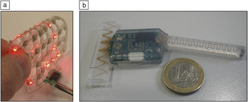
In some cases, the circuit, by nature of its functionality, occupies a large area and contains components that are placed at a certain distance from one another, making miniaturization problematic. One case is a circuit that is a large area network of distributed sensors or electronic components, such as a conformable light source or display consisting of individual LEDs in a matrix arrangement (see Figure 11a)Reference Vervust, Bossuyt, Axisa and Vanfleteren22 or a distributed pressure sensor network for artificial skin applications.Reference Missinne, Van Steenberge, Van Hoe, Van Coillie, Van Gijseghem, Dubruel, Vanfleteren and Van Daele23 Another case is a circuit that has one or more single distant components, such as an electrocardiogram monitoring circuit (Figure 11b),Reference Sterken, Vanfleteren, Torfs, Op de Beeck, Bossuyt and Van Hoof24 where the minimum distance between monitoring electrodes should be 5 cm to 10 cm. The circuit is designed such that the electronics are concentrated around one electrode, while the other (distant) electrode is connected to the circuit using a stretchable conductor.
(a) 7 × 8 light-emitting diode matrix (device size is ∼9 × 9 cm2); (b) wireless electrocardiogram monitor with stretchable antenna and interconnect to distant electrode.Reference Sterken, Vanfleteren, Torfs, Op de Beeck, Bossuyt and Van Hoof24 Note: A one Euro coin is included for scale.

Conclusions and outlook
A technology for stretchable circuits has been developed, allowing the realization of a complete new range of electronic devices featuring conformability as the unique characteristic. Distributed pressure sensor networks for artificial skins, conformable light sources, and randomly shaped soft biomedical implants are only a few application examples. The presented technology has been developed by using standard printed circuit board patterning and assembly methods, together with polymer molding techniques. A straightforward transfer of the technology to an industrial environment is anticipated. It has been shown that mechanical reliability is strongly enhanced by introducing a flexible support material for the meanders and by providing smooth mechanical transitions between the rigid solder assembled standard components and the soft and conformable stretchable interconnects. Future work will include continued improvement of design and technology for these transitions and investigations on how the technology can be transferred to an industrial environment.
Acknowledgments
The authors gladly acknowledge the financial support of this research by the European, Belgian, and Flemish authorities through the following projects: IWT-SBO-BioFlex, BELSPO-TAP2-SWEET, EC-FP6-STELLA, EC-FP7-Place-It, and EC-FP7-PASTA.