Introduction
The rapid advancements in modern wireless technology create a scarcity in the available frequency spectrum. In-band full duplex (IBFD) system is a potential candidate to address this issue where the transmission and reception of message signals are done simultaneously using a single frequency. Theoretically, a full-duplex system can increase the spectrum efficiency two times that of a half-duplex system [Reference Sabharwal, Schniter, Guo, Bliss, Rangarajan and Wichman1]. However, while transmitting and receiving at the same frequency, the interference caused by a strong transmitting signal on a weaker receiving signal is the main concern that needs to be minimized to make the IBFD system more efficient. To address this issue, several self-interference cancellation (SIC) techniques are reported in the literature [Reference Kolodziej, Perry and Herd2]. Generally, SIC techniques are collectively implemented in RF/analog [Reference King, Xia and Boumaiza3], digital [Reference Cheng, Chen, Zhang, Gao, Han, Han, Yu and Deng4], and antenna domains but an antenna system having high inter-port isolation can further decrease the need for SIC in succeeding stages. Various methods such as the use of a circulator [Reference Prasannakumar, Elmansouri and Filipovic5], increased antenna separation [Reference Everett, Sahai and Sabharwal6], near field cancellation [Reference Wu, Zang, Li and Behdad7], and beam-forming network [Reference Ha, Elmansouri, Prasannakumar and Filipovic8] are used for achieving high inter-port isolation. Typically, these techniques involve the use of multiple antennas or complex antenna structures, resulting in a bulky form factor or larger physical dimensions.
Considering simplicity in the design process, dual-polarized antennas are preferred for the IBFD system [Reference Ta and Trong9]. Several dual-polarized antenna structures are reported in the literature [Reference Zhang and Wu10–Reference Yun, Liu, Wu and Lennerstad19] which suffer from one or many of the following disadvantages:
(i) Separate radiators are used for the Transmitter (Tx) and Receiver (Rx) which results in a large footprint [Reference Chaudhary, Jeong and Jeong13, Reference Wang, Tang, Yang and Chen14].
(ii) Isolation less than 40 dB is achieved between Tx and Rx which might not be sufficient for an IBFD system [Reference Zhang and Wu10, Reference Sangam, Poolakkal, Palthiya, Nallam and Kshetrimayum15].
(iii) Impedance bandwidth of the design is limited (<6%) [Reference Prasad, Singh, Tripathi and Paltani11–Reference Sangam, Poolakkal, Palthiya, Nallam and Kshetrimayum15, Reference Nawaz, Basit and Niazi17, Reference Yun, Liu, Wu and Lennerstad19].
(iv) Peak gain of the design is limited (∼5dBi) [Reference Nawaz, Ahmad and Aslam12, Reference Wang, Tang, Yang and Chen14, Reference Yun, Liu, Wu and Lennerstad19].
Also, the higher-order modes of an antenna can cause electromagnetic interferences to the different devices of any wireless communication system. Hence, to suppress undesired higher-order modes of the antenna, several research activities have been proposed in recent times. These include exciting a circular patch with common mode signals [Reference Zhang, Zhu, Wu, Liu and Wu20], loading of shorting pins [Reference Huang, Zhu and Zhang21], deploying a pair of λ/4 resonators with capacitive feed [Reference Pozar22], and use of multi-point differential feed [Reference Nishiyama, Aikawa and Egashira23], etc.
The above discussion clearly indicates that all the previous works are designed either for the IBFD applications or for the suppression of higher-order modes. To the best of the authors’ knowledge, it is the first instant a shared radiator-based wideband IBFD antenna with enhanced isolation is presented which can simultaneously suppress the higher-order modes. The major contributions of the proposed work are as follows:
1) To the best of the authors’ knowledge, it is the first instance that dual differential capacitive feeding is proposed to implement a wideband IBFD antenna. This proposed feeding scheme has three major functions: (i) suppression of all second-order higher modes; (ii) creation of dual resonance behavior that can be transformed into wideband performance; (iii) enhancement of the inter-port isolation.
2) A mathematical model is presented to illustrate the effect of the double differential feeding on inter-port isolation.
3) To the best of the authors’ knowledge, our proposed design is the first dual-polarized IBFD antenna that not only provides stellar full duplex performance (excellent inter-port isolation of greater than 58 dB over a wideband of 20% with significant peak gain of 9.1 dBi) but also suppresses all the spurious second-order higher modes. To suppress higher order modes, we have not employed any filtering circuits (LPF, BPF, BSF) that would increase the overall footprint, defected ground structures that have back radiations, or complex electronic bandgap structures.
4) The functionality of the proposed IBFD antenna is validated through the lumped equivalent circuit model. Moreover, the effectiveness of the proposed circuit model is validated through the parametric studies where the results obtained through circuit simulation closely resemble the EM simulation results.
Antenna configuration
The geometry of the proposed dual-polarized IBFD antenna is depicted in Fig. 1. It consists of two square microstrip patches which are built on Rogers RT 5880 substrate (εr = 2.2, tan δ = 0.0009) of thickness 1.575 mm. The radiating patch (RP), built on substrate 2 is excited with dual differential feeding. Port 1+ and 1– are used as differential Tx ports while port 2+ and 2– are used as differential Rx ports. The feeding of RP through each differential port is done with the help of a pair of λ/4 resonators. A metallic pin having a diameter dia is placed at the center of the feedline which is shorted to the ground. The parasitic patch (PP) is placed above RP at a height of h on substrate 1. The ANSYS Electronics Desktop (HFSS) is used to design and optimize the structure.
Proposed design with dimensions (in mm): (a) 3 d view, (b) top view of the bottom layer; l s = w s = 100, W 1 = 37, W 2 = 38.2, l r = 19.2, w f = 4.5, wr = 1.75, d = 1, dia = 0.3, h = 10.

Operational mechanism
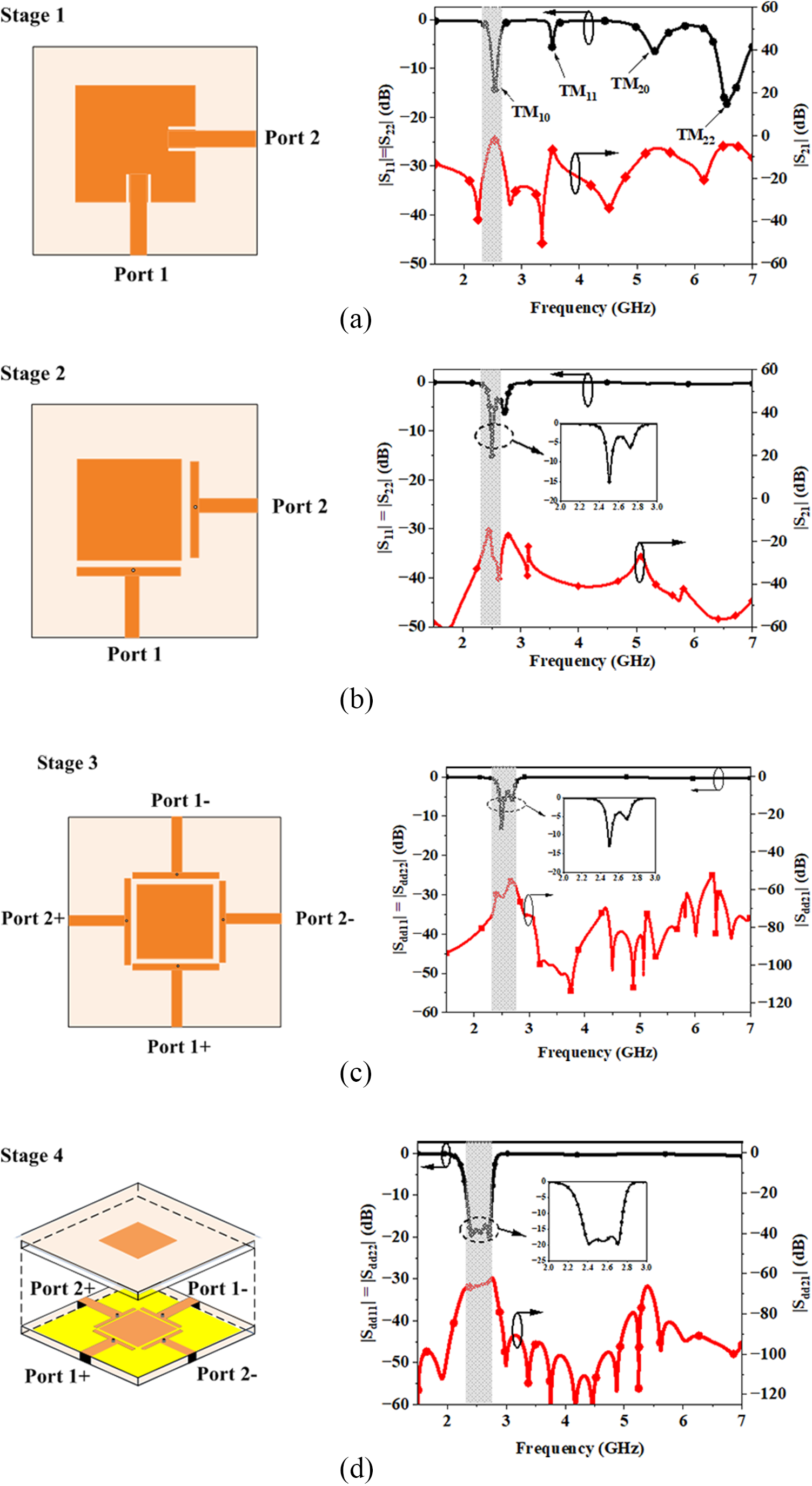
Theoretically, a dual-polarized antenna where Tx and Rx have orthogonal polarization, has infinite isolation between the Tx and Rx port, a favorable condition for the IBFD system. Hence, at Stage 1, a dual-polarized square MPA is excited through direct feeding (insert-fed) at port 1 (Tx port) and port 2 (Rx port). The feeding arrangement shown in Fig. 2(a) ensures that the Tx port is orthogonally polarized with respect to the Rx port. This MPA resonates at a center frequency (f 0) of 2.5 GHz. It is evident from the S-parameters shown in Fig. 2(a) that in addition to fundamental mode TM 10 (2.5 GHz) of this MPA, other higher order modes TM 11 (3.55 GHz), TM 20 (5.3 GHz) and TM 22 (6.7 GHz) also exist.
Design evolution of the proposed IBFD antenna and simulated s-parameters: (a) stage 1, (b) stage 2, (c) stage 3, (d) stage 4.

Now, instead of direct feeding, capacitive feeding with the help of pairs of λ/4 resonators is provided to the MPA as shown in Stage 2 of Fig. 2(b). This configuration results in spurious-free characteristics as shown in Fig. 2(b). The suppression of higher-order modes is due to the presence of pairs of λ/4 resonators which are centrally loaded with a shorting pin [Reference Pozar22].
The non-radiating λ/4 resonators along with a shorting pin exhibit resonance at discrete frequencies (nf 0, where n = 1, 3, .. (2 N + 1)). The MPA is capacitively fed by λ/4 resonators, allowing energy transmission only at discrete frequencies where both the λ/4 resonators and MPA resonate simultaneously. Consequently, it is not possible to excite higher-order modes like TM 11 and TM 22 due to their resonance frequencies not being a multiple of f 0. For a square MPA, the resonant frequency of the TM 11 and TM 22 modes are 1.414 f 0 and 2.828 f 0, respectively.
In addition, the placement of a shorting pin at the center of a feedline results in the creation of an electric field null at the center plane. This configuration prevents the excitation of even order modes, such as TM 20, because the primary requirement to excite any even order mode is to have an electric field maximum in the central plane. Hence, this feeding mechanism shown in Stage 2 of Fig. 2(b) successfully suppresses the second-order modes which are the most critical in any communication system. In spite of good out-of-band performance, this configuration has inter-port isolation of 20 dB as shown in Fig. 2(b) which is insufficient for an IBFD system.
Further, to increase the inter-port isolation, differential feeding is provided to Tx and Rx ports which is presented as Stage 3 of Fig. 2(c). To understand the effect of this double differential feeding on inter-port isolation in more detail, a mathematical model is developed based on the analysis proposed in [Reference Chaudhary, Jeong and Jeong13]. To apply the differential feed at both the Tx and Rx ports, two different hybrid couplers can be utilized as shown in Fig. 3. Here, the current at Port 1(Tx) and Port 2(Rx) is represented as I1 and I2 respectively. Assuming the lossless hybrid coupler (H.C.), the output currents of H.C. 1 can be written as [Reference Pradhan, Subramanian, Barik and Cheng24]
 \begin{equation}{I_{1 + }} = \frac{1}{{\sqrt 2 }}{I_1}{\text{ }}and{\text{ }}{I_{1 - }} = - \frac{1}{{\sqrt 2 }}{I_1}{\text{ }}\end{equation}
Stage 3 antenna having dual differential feedings realized using identical hybrid couplers.

As the differential port 2 is acting as a receiver port, different currents of H.C. 2 are related to each other as follows:
 \begin{equation}{I_2} = \frac{1}{{\sqrt 2 }}({I_{2 + }} - {\text{ }}{I_{2 - }})\end{equation}
Now, let the mutual coupling between port 2+ (2-) and port 1+(1-) is represented as S2 +1 + (S2-1-) and S2 +1– (S2-1 +) denotes the mutual coupling between port 2+ (2–) and port 1– (1+), then
 \begin{equation*}{I_{2 + }} = \frac{{{I_1}}}{{\sqrt 2 }}{S_{2 + 1 + }} - {\text{ }}\frac{1}{{\sqrt 2 }}{I_1}{\text{ }}{S_{2 + 1 - }}\end{equation*}
 \begin{equation} = \frac{{{I_1}}}{{\sqrt 2 }}[{S_{2 + 1 + }} - {\text{ }}{S_{2 + 1 - }}]\end{equation}
 \begin{equation}{I_{2 - }} = \frac{{{I_1}}}{{\sqrt 2 }}[{S_{2 - 1 + }} - {\text{ }}{S_{2 - 1 - }}]\end{equation}
Now using eq. (2), (3) and (4), I 2 can be found as
 \begin{equation}{I_2} = \frac{{{I_1}}}{2}\left[ {({S_{2 + 1 + }} - {\text{ }}{S_{2 + 1 - }}} \right) - \left( {{S_{2 - 1 + }} - {\text{ }}{S_{2 - 1 - }}} \right)]\end{equation}
Therefore, based on Eq. (5) the relationship between the current of port 1 and 2 can be expressed as
 \begin{equation}\frac{{{I_1}}}{{{I_2}}} = \frac{2}{{\left[ {({S_{2 + 1 + }} - {\text{ }}{S_{2 + 1 - }}} \right) - \left( {{S_{2 - 1 + }} - {\text{ }}{S_{2 - 1 - }}} \right)]}}\end{equation}
The proposed structure is symmetrical and considering the ideal differential operation performed by the hybrid couplers, the coupling between the orthogonally placed ports will be identical ( ${S_{2 + 1 + }} = {\text{ }}{S_{2 + 1 - }} = {S_{2 - 1 + }} = {\text{ }}{S_{2 - 1 - }}$). Hence, it is evident from Eq. (6) that theoretically, infinite inter-port isolation is achieved using this configuration. Nevertheless, in practical use, significantly large inter-port isolation can be achieved by utilizing highly precise hybrid couplers that produce output signals with equal magnitude and out-of-phase characteristics [Reference Chaudhary, Jeong and Jeong13].
It is important to note that double differential feeding deployed at Stage 3 is the major factor in achieving high inter-port isolation. The differential operation performed at the Tx port is responsible for suppressing any Tx-Rx leakage at Rx ports while the differential Rx ports subsequently suppress any further residual self-interference. Hence, the polarization diversity along with double differential feeding yields a high inter-port isolation better than 60 dB for the entire operating band as shown in Fig. 2(c).
The surface currents for Tx and Rx ports are shown in Fig. 4. It is evident that the surface current is oriented in the x (y) direction when differential Tx (Rx) ports are excited while the Rx (Tx) ports are terminated with a matched load. Even though high inter-port isolation is achieved at this design stage, the input matching of this stage is very poor, and impedance bandwidth (|S 11| < − 10 dB) is limited (∼40 MHz).
Distribution of surface current on the RP: (i) when differential Tx ports are excited and Rx ports are terminated with matched load, (ii) when differential Rx ports are excited and Tx ports are terminated with matched load.

Although the dual resonant behavior can be observed in antennas of Stage 2 and Stage 3 due to close proximity of λ/4 resonators with the RP (Fig. 2(b) and Fig. 2(c)), the input matching and impedance bandwidth are not sufficient. Therefore, a PP is placed above the RP in Stage 4 as shown in Fig. 2(d). The inclusion of PP has two-fold utility; first, it improves the input matching and then it also improves the impedance bandwidth. It is clear from the S-parameters shown in Fig. 2(d) that the Stage 4 antenna results in a high isolation of 65 dB over the entire operating frequency band (2.30–2.76 GHz).
To illustrate the improvement in input matching, the input impedances of Stage 3 and Stage 4 antennas are plotted in Fig. 5(a). It clearly shows that the Stage 3 antenna exhibits inadequate input matching over the desired operating band.
Now, the air gap between RP and PP facilitates the mixed coupling (electric and magnetic couplings) [Reference Nishiyama, Aikawa and Egashira23]. The effect of this mixed coupling can be observed in Fig. 5(a). This mixed coupling offers either inductive or capacitive impedance across different frequencies. Consequently, an air gap of varying height results in a substantial change in input impedance (the corresponding parametric study is shown in the Section V of this paper). Hence, with the placement of the PP above RP at an optimal height (h) of 10 mm, the imaginary part of Zdd 11 of the Stage 4 antenna approaches zero, while the real component of Zdd 11 is near to 50 Ω in the entire operating band. This demonstrates the significant improvement of input matching resulting from the strategic placement of PP at an optimal height of h.
(a) Input impedance matching of stage 3 and stage 4 antenna, (b) Smith chart for impedance matching of stage 3 and stage 4 antenna.

Additionally, the excellent input matching for the entire operating band is also reflected in the Smith Chart shown in Fig. 5(b). The impedance loop of the Stage 4 antenna evidently shifts towards the center of Smith chart which further confirms the substantial improvement in the matching performance due to PP being placed above the RP at a height of h.
Further, the judicious selection of the air gap (h) as 10 mm (∼0.1 λ) facilitates the fundamental mode of PP to resonate with close proximity of the fundamental mode of RP [Reference Naseri, PourMohammadi, Melouki, Ahmed, Iqbal and Denidni25]. Thus, the improved impedance bandwidth (460 MHz) is achieved because three different structures i.e. RP, PP, and λ/4 resonators are resonating in close vicinity. This Stage 4 antenna presented in Fig. 2(d) is our proposed IBFD antenna which has significantly large inter-port isolation over a wide frequency range. Also, this design successfully suppresses the higher-order modes which can be undesirable for other surrounding devices. Table 1 summarizes the key characteristics of antennas of different stages which clearly highlight the achievement of performance improvement of the proposed IBFD antenna in successive stages.
Key features of antennas of different stages

Equivalent lumped circuit model
To gain further insight into the proposed design, an equivalent lumped circuit model of the proposed dual-polarized IBFD antenna is presented in Fig. 6. The differential feeding is provided at both Tx and Rx ports through a microstrip line of characteristic impedance Z 0. The λ/4 resonator is modeled as a lossless LC circuit (Lri, Cri, i varying from 1 to 4). These pair of λ/4 resonators at the Tx and Rx ends are connected in parallel. At one end, these resonators are connected to shorting pins shown as Lpin 1 and Lpin 2 at the Tx and Rx ends, respectively. The gap between the feeding circuit and the RP is modeled as a π-network of three capacitances Cg 1, Cg 2, Cg 3 and Cg 4, Cg 5, Cg 6 at Tx, and Rx ends, respectively. A combination of two parallel RLC circuits i.e. R 1L 1C 1 and R 2L 2C 2 is used to represent the RP when it is excited at differential Tx and Rx ports respectively. It is important to note that, the RP is operating under TM10 mode when excitation is provided at differential port 1 while the dominating mode of operation is TM01 when RP is excited at differential port 2. Similarly, the PP is presented as a parallel resonant circuit Rp1Lp1Cp1 and Rp2Lp2Cp2 when it is excited with differential port 1 and differential port 2, respectively. The resonant frequency  $({f_r})$ of each of the three resonators (RP, PP, and λ/4 resonators) can be calculated with the following relation:
 \begin{equation}{f_r} = \frac{1}{{2\pi \sqrt {{L_r}{C_r}} }}\end{equation}
where L r and C r represent the inductance and capacitance of the corresponding resonator.
Lumped circuit equivalent model of the proposed antenna:  ${L_{pin1}} = {L_{pin2}} = 72.5{\text{ }}nH,{\text{ }}{L_{r1}} = {L_{r2}} = {L_{r3}} = {L_{r4}} = 0.82{\text{ }}nH,{\text{ }}{R_1} = {R_2} = 328{\text{ }}\Omega, {\text{ }}{C_{r1}} = {C_{r2}} = {C_{r3}} =$
 ${C_{r4}} = 4.14{\text{ }}pF,{\text{ }}{C_{g1}} = {C_{g4}} = 1.77{\text{ }}pF,{\text{ }}{C_{g2}} = {C_{g3}} = {C_{g5}} = {C_{g6}} = 0.28{\text{ }}pF$,
 ${L_1} = {L_2} = 0.95{\text{ }}nH,{C_1} = {C_2} = 4.94{\text{ }}p$F,
 ${L_{c1}} = {L_{c2}} = 0.23{\text{ }}nH$
 ${C_{c1}} = {C_{c2}} = 12.86{\text{ }}pF$,
 ${R_{p1}} = {\text{ }}{R_{p2}} = 15{\text{ }}\Omega $,
 ${L_{p1}} = {L_{p2}} = 0.28{\text{ }}nH$,
 ${C_{p1}} = {C_{p2}} = 13.37{\text{ }}pF$.

Further, the mixed coupling (combination of electric and magnetic coupling) between the RP and PP is described as two parallel LC circuits (LC 1, CC 1 and LC 2, CC 2). Finally, the mutual coupling between port 1 and port 2 is defined as M12 [Reference Zhang, Ke, Wang, Tang and Chen26,Reference Chen, Ye, Liu and Wu27]. The working mechanism of various components used in the circuit model can be understood by comparing them with the actual elements utilized in the design of the IBFD antenna as tabulated in Table 2. In addition, the ADS software is utilized to design and validate the IBFD antenna equivalent circuit model. A comparison of simulated results obtained from ADS and HFSS is presented in Fig. 7, demonstrating a high level of consistency between the two.
Comparison between EM simulation and circuit simulation of the proposed IBFD antenna: (a) magnitude plot (b) phase plot (unwrapped).

Relationship of circuit elements used in ADS simulation with their counterpart in EM simulation

Parametric analysis
To elucidate the impact of a few parameters on the performance of the proposed IBFD antenna, two parametric studies are performed. The first study illustrates the effect of variations in d (the gap between a pair of λ/4 resonators and RP) on the input reflection coefficient, as depicted in Fig. 8 (a). For a nominal value of d as 1 mm, all the three reflection poles due to RP, PP, and λ/4 resonators are combined to form a wideband antenna. When the value of d is increased to 1.3 mm, all the reflection poles are merged into a single reflection pole. Additionally, to validate the effectiveness of the proposed equivalent circuit model, one capacitor (Cg1) of the π network (the circuit equivalent of the gap (d) between a pair of λ/4 resonators and RP) is varied and its effect on input reflection coefficient is presented in Fig. 8 (b). It is evident from the Fig. 8 that both EM and circuit simulation leads to a similar conclusion. It is important to note that all parameters except d (Cg1) in EM (circuit) simulation are maintained constant in the aforementioned study.
The effect of variations in (a) d (b) Cg1 on the input reflection coefficient.

Subsequently, in another parametric study, the effect of variations in the air gap (h) between RP and PP is analyzed, as shown in Fig. 9(a). It clearly demonstrates that the judicious selection of the airgap (h) as 10 mm is essential for the fundamental mode of PP to resonate with close proximity of the fundamental mode of RP which results in a good impedance matching over a wideband. Furthermore, as discussed in the previous section, the air gap between RP and PP facilitates the mixed coupling (electric and magnetic couplings) to improve the input matching. This can be further verified from the parametric variation in C c1 (parallel combination of C c1 and L c1 is circuit equivalent to mixed-coupling provided by the air gap between RP and PP) performed in circuit simulation as shown in Fig. 9(b). Hence, the prudent selection of air gap to obtain a good input matching over a wideband is justified with the help of EM and circuit simulation as illustrated in Fig. 9.
The effect of variations in (a) h (b) cc1 on the input reflection coefficient.

Results and discussion
To validate the functionality of the proposed design, a prototype is implemented using RT Duroid substrate, and the nylon screws are used to hold both substrate layers. The fabricated prototype is shown in the inset of Fig. 10(a). To provide differential signals at Tx and Rx ports, an ultra-wideband hybrid coupler proposed in [Reference Ta and Trong9] is used. The magnitude and phase imbalance between the two output ports of this coupler is within the limit (±0.2 dB and ±2.5◦ respectively) over a large frequency range (1–10 GHz).
Measured results of the proposed IBFD antenna: (a) out of band performance, (b) reflection coefficients and inter-port isolation, (c) realized gain, (d) e-plane and h-plane radiation pattern of Tx port at (i) 2.4 Ghz (ii) 2.65 Ghz.

The S − parameters of the proposed dual-polarized IBFD antenna are measured using the Agilent Vector Network Analyzer [N5247A] and presented in Fig. 10. The improved out-of-band characteristic of the proposed structure can be observed in Fig. 10(a) which clearly shows that it possesses spurious free characteristics. Moreover, as shown in Fig. 10(b), the measured impedance bandwidth is ∼20% (2.26–2.76 GHz) which is somewhat larger than the simulated results. Also, the measured isolation between Tx and Rx ports is better than 58 dB for the entire operating range (2.26–2.76 GHz) while in simulation it was obtained as 65 dB. The discrepancies between the simulated and measured results are due to cable losses and misalignment of the PP with respect to the driven patch.
The far-field parameters are measured in an anechoic chamber and the measured realized gain and radiation pattern are presented in Fig. 10(c) and Fig. 10(d), respectively. It is important to note that the proposed design is symmetrical with respect to Tx and Rx ports. Thus, the measured results are presented only for the differential Tx ports for brevity. The peak values of measured realized gain and radiation efficiency are 9.1 dBi and 92%, respectively. The cross-polarization better than −30 dB at boresight direction is measured at two operating frequencies 2.4 GHz and 2.65 GHz in both E and H planes. It is evident from the measured results that these are in close agreement with the simulated results.
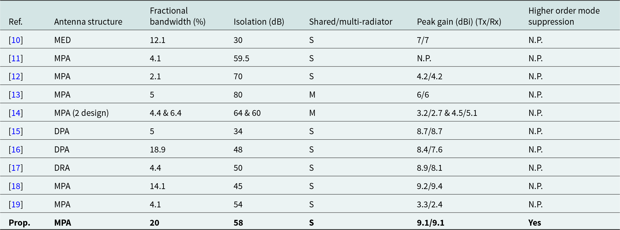
A detailed comparison of the proposed structure with other reported dual-polarized IBFD antennas is presented in Table 3. The present design offers the largest fractional bandwidth (|S 11| < −10 dB) of 20% among all the designs listed in Table 3. Though the designs presented in [Reference Chaudhary, Jeong and Jeong13] and [Reference Wang, Tang, Yang and Chen14] offer better inter-port isolation, these multi-radiator-based designs have very narrow bandwidths and possess lower values of peak gain. Moreover, none of the aforementioned IBFD structures provide suppression of higher-order modes. Hence, it can be concluded that the proposed shared radiator-based design provides significantly larger isolation of 58 dB over a wide bandwidth of 20% along with a large peak gain of 9.1 dBi and an excellent out-of-band performance.
Comparison of the proposed work with reported works

DPA: Dielectric Patch Antenna, DRA: Dielectric Resonator Antenna, MED: Magneto Electric Dipole, N.P.: Not Provided
Conclusion
In this paper, a wideband IBFD antenna is presented which is also capable of suppressing higher-order modes. The employability of λ/4 resonators along with PP in wideband operation. An isolation better than 58 dB between the Tx and Rx ports is achieved due to orthogonally polarized surface currents applied through a balanced feed to the Tx and Rx ports. The key attributes of the proposed design are simplicity in design, very high isolation over a large frequency band, and excellent out-of-band performance. Due to these features, the proposed design not only provides excellent performance in the ISM band but can also be scaled to higher frequency bands.
Data availability statement
Data sharing is not applicable to this article as no data sets were generated or analyzed during this study.
Acknowledgements
The authors acknowledge the Department of Electronics and Communication Engineering, Indian Institute of Technology Roorkee, Uttarakhand, India, for providing equipment and laboratory facilities to carry out this work.
Funding statement
This research received no specific grant from any funding agency, commercial or not-for-profit sectors.
Competing interests
The authors report no conflict of interest.

Sandeep Rana received his M.Tech. degree from Delhi Technological University, New Delhi, India, in 2014. He is presently enrolled as a full-time Ph.D. research scholar in the Department of Electronics & Communication Engineering at the Indian Institute of Technology Roorkee, Uttarakhand, India. He is on academic leave from his position as an Assistant Professor in the ECE Department at G. B. Pant Institute of Engineering and Technology (GBPIET), Uttarakhand, where he has been serving as a faculty member since 2019. Prior to his tenure at GBPIET, he served as a faculty member at Graphic Era Hill University, Dehradun, and Netaji Subhash Institute of Technology, New Delhi, India. He has nine publications till date including four journal and five conferences. His research interests revolve around the design of microwave circuits and antennas tailored for modern wireless communication applications.

Amit Kumar is currently pursuing his Ph.D. from Electronics and Communication Engineering (ECE) Department, Indian Institute of Technology Roorkee, India. He completed his M.Tech in ECE Department at National Institute of Technology Warangal, India, in 2022. He has worked as research intern at Wipro, India during his M.Tech. His current areas of research include design of linear and efficient RF Power amplifiers, design of microwave circuits and antennas for V2X communication. He has five publications till date.

Akhilesh Mohan received the B.Tech. degree in Electronics Engineering from Kamla Nehru Institute of Technology, Sultanpur, India, in 2002, the M.Tech. degree and Ph.D. degree in Microwave Engineering from Indian Institute of Technology Kanpur, Uttar Pradesh, India, in 2004 and 2009, respectively. From 2009 to 2010, he worked as a Scientist at Space Applications Center, Indian Space Research Organization, Ahmedabad, India. From 2010 to 2013, he was a faculty member with the Department of Electrical Engineering at Indian Institute of Technology Jodhpur, Rajasthan, India. From 2013 to 2020, he was a faculty member with the Department of Electronics and Electrical Communication Engineering at Indian Institute of Technology Kharagpur, West Bengal, India. Since 2021, he has been a faculty member with the Department of Electronics and Communication Engineering at Indian Institute of Technology Roorkee, Uttarakhand, India. Dr. Mohan has authored and co-authored more than 150 peer reviewed international journals and conference papers. His research interests include the design of microwave filters, antennas, and absorbers for wireless communication systems.