Introduction
The electronic and mechanical properties of two-dimensional (2D) materials have showed potential to overcome the drawbacks of conventional electronics in moving toward mechanically flexible/stretchable applications for lightweight, portable, and conformable products such as flexible displays, solar cells and batteries, and wearable health patches. Reference Novoselov, Fal’ko, Colombo, Gellert, Schwab and Kim1 In spite of the very good properties of graphene, the zero-energy bandgap in its electronic structure makes it unsuitable for switching devices in electronics. Recently, 2D layered semiconductors, in particular, the series of transition-metal dichalcogenides (TMDCs) such as MoS2 and WSe2, have shown reliable performance as novel semiconductor materials that can provide mechanical flexibility and high mobility. Reference Radisavljevic, Radenovic, Brivio, Giacometti and Kis2 While the potential of 2D layered materials is exciting, major roadblocks will have to be resolved for successful transition to commercial applications by developing reliable technologies for the controlled fabrication of high-performance devices (e.g., gate width of ∼10 nm for TMDC-based field-effect transistors with high ON-OFF current ratios, Reference Yoon, Ganapathi and Salahuddin3 reliable means to control the number of TMDC layers for bandgap tuning, Reference Castellanos-Gomez, Barkelid, Goossens, Calado, van der Zant and Steele4 on-demand tuning of electronic properties by defect engineering, Reference van der Zande, Huang, Chenet, Berkelbach, You, Lee, Heinz, Reichman, Muller and Hone5 and maskless patterning of 2D layered materials).
Ultrafast lasers offer unique processing routes that take advantage of distinct interaction mechanisms with 2D materials to enable extremely localized energy deposition. Both thermal and non-thermal mechanisms can contribute to the processing of layered materials, depending on the amount of energy absorbed. Reference Currie, Caldwell, Bezares, Robinson, Anderson, Chun and Tadjer6 For femtosecond laser processing of graphite, time-of-flight measurements have confirmed that femtosecond laser-driven Coulomb explosion (i.e., ionization assisted non-thermal ablation mechanism) is responsible for atomic-scale material removal from graphite, suppressing subsequent thermal material ejection. Reference Lenner, Kaplan, Huchon and Palmer7,Reference Lenner, Kaplan and Palmer8 It is also noted that atomic-scale material removal from layered materials by ultrafast lasers is frequently coupled with chemical reactions such as oxidation or burning, as in the case of graphene. Reference Stohr, Kolesov, Xia and Wrachtrup9 It is believed that such a disturbance can lead to non-thermal bond breaking and even stochastic extraction of atoms from layered materials. The reduced in-plane thermal conductivity tends to accelerate the process thus partly contributing to high spatial confinement of the process. Reference Stohr, Kolesov, Xia and Wrachtrup9
Similar bond-breaking behavior upon interaction with ultrafast lasers has been observed for MoS2 layers, where precise layer removal or thinning can actively adjust its bandgap. In this case, a lattice sublimation mechanism (i.e., laser-induced bond breaking and subsequent atom removal) was proposed, possibly assisted by a non-thermal ionization state rather than by oxidation. Reference Paradisanos, Kymakis, Fotakis, Kioseoglou and Stratakis10 It is interesting to note that atomic-scale vacancies formed in MoS2 by high-energy electrons (in a high-resolution transmission electron microscope environment) are easily refilled with impurity atoms, Reference Komsa, Kotakoski, Kurasch, Lehtinen, Kaiser and Krasheninnikov11 suggesting a new method for defect engineering or doping of TMDC materials. This study indicates that further investigation of the effect of ultrafast lasers in terms of atomic-scale defect formation is necessary with advanced in situ diagnostics tools, as will be briefly discussed in later sections. It is also noted that a wider range of ultrafast laser- (typically a femtosecond or picosecond laser that can selectively induce non-thermal or thermal mechanisms) based modification processes such as ablative, additive, and defect engineering processes, are governed by closely linked mechanisms (e.g., non-thermal bond-breaking possibly accompanied by defect engineering or doping).
The nonlinear ultrafast optical properties of 2D layered materials have been actively investigated for photonic device applications. Reference Wang, Wang, Fan, Lotya, O’Neill, Fox, Feng, Zhang, Jiang, Zhao, Zhang, Coleman, Zhang and Blau12 Accordingly, the nonlinear absorption behavior has been examined during ablative processing of layered materials; two-photon absorption was confirmed during ablation of MoS2. Reference Stohr, Kolesov, Xia and Wrachtrup9 Since the heat dissipation of 2D layered materials is dominantly influenced by thermal coupling to the surrounding environment, a dependence of the processing threshold in terms of laser fluence or energy density on the substrate material was also found. The underlying thin-film or substrate material can be incorporated into the layered materials, as shown in experimental work on localized laser synthesis of graphene. Reference Currie, Caldwell, Bezares, Robinson, Anderson, Chun and Tadjer6,Reference Wei, Mitchell, Tansarawiput, Nam, Qi, Ye and Xu13 Considering the precise and unique energy coupling mechanisms with 2D layered materials, more accurate thickness control is anticipated by using ultrafast lasers.
The following sections summarize research on ultrafast laser-based processing of 2D atomic layered materials, including ablative patterning and thinning, substitutional doping, and additive direct writing. The article concludes with an outlook toward advanced processing and in situ diagnostics.
Ablative patterning and pattern transfer of graphene by ultrafast lasers
In graphene device fabrication, typically a synthesized graphene layer on a metal foil is transferred to a target substrate, followed by patterning. However, these processes involve wet chemical steps and can unintentionally modify the graphene properties. Reference Pirkle, Chan, Venugopal, Hinojos, Magnuson, McDonnell, Colombo, Vogel, Ruoff and Wallace14,Reference Cheng, Zhou, Wang, Li, Wang and Fang15 Furthermore, most of the transferred graphene area is etched away during the patterning step, so little area is used. Hence there is room for improvement in current graphene fabrication methods.
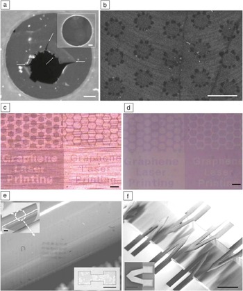
Femtosecond laser-ablative patterning of suspended and supported graphene under ambient conditions is summarized in Figure 1 . Reference Yoo, In, Park, Jeon and Grigoropoulos16 Direct ablation was observed upon single pulse irradiation of suspended graphene (Figure 1a), wherein graphene folds were formed in the periphery of ablated supported graphene spots (Figure 1b). Multiscale graphene patterns have been also transferred to arbitrary substrates by applying femtosecond laser pulses on a graphene/metal foil prior to the transfer step (Figure 1c–d). The diminished thermal transport accompanying femtosecond laser processing enables formation of high-resolution graphene patterns, even on thermally conductive metal foil. Reference Park, Yoo and Grigoropoulos17 Furthermore, a laser-induced pattern transfer (LIPT) method was developed. Femtosecond laser patterning is performed on a graphene/poly(methyl methacrylate) (PMMA) donor layer, and the patterned graphene is simultaneously transferred to a target substrate. This results in the simultaneous patterning and transfer of graphene in a single processing step. The LIPT method simplifies the complex graphene fabrication process while augmenting flexibility in graphene device design. Graphene/PMMA microscale patterns on a flexible substrate (Figure 1e) and suspended graphene cantilever structures were fabricated via the developed single-step method (Figure 1f). Reference Yoo, Park, Ahn and Grigoropoulos18
Direct laser patterning of graphene. (a) Scanning electron microscope (SEM) image of a single pulse irradiated suspended single-layer graphene on a transmission electron microscope grid. Arrows indicate cracks developed by ablation. The inset shows a pristine suspended graphene. The scale bar indicates 200 nm. (b) SEM image of folded graphene structures on a SiO2/Si substrate. Reference Yoo, In, Park, Jeon and Grigoropoulos16 The scale bar indicates 2 μm. Optical micrographs of (c) various graphene patterns on a graphene/copper foil after femtosecond laser patterning and (d) transferred graphene patterns on a SiO2/Si substrate. Scale bars are 100 μm. (e) Optical microscope image of transferred graphene/poly(methyl methacrylate) (PMMA) patterns on a flexible polyimide film over a curved surface. The entire view is shown in the upper inset. The bottom inset shows a transferred pattern with higher magnification. (f) Tilted SEM image of graphene/PMMA cantilevers over a trench in a silicon substrate. The inset shows a SEM top view image of the cantilever pattern. Reference Yoo, Park, Ahn and Grigoropoulos18 Scale bars in (e–f) are 200 μm.

Direct nanoscale patterning of suspended and supported graphene has been demonstrated, where a vortex phase plate beam shaping technique was applied to achieve resolution down to 20 nm. Reference Stohr, Kolesov, Xia and Wrachtrup9 When graphene is patterned into nanoribbon shapes, an energy gap is created due to quasi-one-dimensional carrier confinement. Reference Han, Ozyilmaz, Zhang and Kim19 By employing high repetition rate ultrafast lasers, precise graphene patterning was achieved due to local oxidation and conversion into CO2. Based on Raman spectroscopy, the defect-induced D-line was not detected after the patterning, indicating that high-atomic-structure quality was maintained in the atomic scale even at the cut edges. Hence direct patterning of graphene using ultrafast pulse lasers is a promising technique for nanoscale graphene fabrication, enabling defect engineering at the nanoribbon edges, which could be free from unintended contamination.
Laser thinning of 2D layered materials
TMDCs are attractive 2D layered semiconductor materials that have unique mechanical, electrical, and optical properties. Reference Wang, Kalantar-Zadeh, Kis, Coleman and Strano20 For example, monolayer MoS2 has a direct bandgap of ∼1.85 eV instead of the indirect bandgap of 1.2 eV for the bulk counterpart. A tightly focused continuous-wave laser beam was utilized to thin MoS2 down to a single layer. Reference Castellanos-Gomez, Barkelid, Goossens, Calado, van der Zant and Steele4 A similar approach was also applied to process multilayer graphene for obtaining single-layer graphene. Reference Han, Chae, Kim, Gunes, Lee, Lee, Lee, Lim, Jeong, Jeong and Lee21 Although laser light may be absorbed in both mono- and multilayered materials, the thinning process is self-regulated due to the variation of the thermal conductivity with the number of layers in conjunction with the heatsink effect of the substrate. The MoS2 thinning process can be further controlled by choosing the appropriate laser wavelength and by using ultrafast pulses, shorter than ∼1 ps. Multilayer MoS2 is opaque to near-infrared Ti:Sapphire femtosecond laser radiation. In contrast, single-layer MoS2 is transparent, implying potential for selective-layer processing. A two-photon absorption process was experimentally confirmed in the course of the ultrafast laser-based MoS2 thinning process. Reference Paradisanos, Kymakis, Fotakis, Kioseoglou and Stratakis10
Ultrafast laser direct writing of graphene patterns
Although pattern-transfer approaches have demonstrated high-quality graphene patterning capabilities, these methods involve multiple processing steps and may cause structural damage during graphene transfer. To resolve these issues, researchers must address these key challenges with the development of direct and transfer-free writing of graphene on desired substrates. To this end, laser direct-writing methods such as laser-induced thermal reduction of graphene oxide (GO) films, Reference Zhou, Bao, Varghese, Tang, Tan, Sow and Loh22,Reference Zhang, Guo, Wei, He, Xia, Chen, Sun and Xiao23 or laser-assisted chemical vapor deposition (CVD), Reference Park, Xiong, Gao, Qian, Xie, Mitchell, Zhou, Han, Jiang and Lu24,Reference Park, Xiong, Xie, Gao, Qian, Mitchell, Mahjouri-Samani, Zhou, Jiang and Lu25 have been examined. However, the laser-induced thermal reduction of GO films yields a substantial number of defects, significantly deteriorating electrical conductivity. The quality of the graphene pattern by laser-assisted CVD on Ni foils was significantly improved over that of thermally reduced GO, Reference Park, Xiong, Xie, Gao, Qian, Mitchell, Mahjouri-Samani, Zhou, Jiang and Lu25 yet a postgrowth graphene-transfer process (i.e., etched removal from Ni foil, then transferred to the target substrate) was necessary.
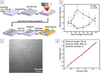
Ultrafast laser direct writing has been employed for directly growing graphene patterns on various insulating substrates under ambient conditions through rapid heating of cosputtered Ni/C thin films (the detailed process sequence is depicted in Figure 2a). Reference Xiong, Zhou, Hou, Jiang, Gao, Fan, Jiang, Silvain and Lu26 The sheet resistance of the resulting graphene patterns is approximately two times lower than the bilayer graphene fabricated by the laser-assisted CVD and one order of magnitude lower than that for the reduced GOs, possibly enabled by the preservation of a high-quality graphene lattice by the transfer-free growth process, and a Ni doping effect. Reference Giovannetti, Khomyakov, Brocks, Karpan, van den Brink and Kelly27,Reference Rigo, Martins, da Silva, Fazzio and Miwa28 The as-measured optical transmittance was 94.3% at 550 nm, supporting potential use as a transparent electrode.
Direct writing of graphene patterns by a femtosecond laser. (a) Process sequence of femtosecond laser direct-writing process to fabricate graphene patterns under ambient conditions. (b) Dependence of the graphene quality (Raman D/G and 2D/G ratios; G band induced by in-plane vibrational mode, D band by defect or disorder, and 2D band by the second-order defect) on laser average powers. At an optimal laser power of 24 mW, a minimal D/G ratio indicates high-quality crystallinity, and a 2D/G ratio close to 1 confirms formation of bilayer graphene. (c) Optical micrograph of large-scale graphene patterns on a glass substrate fabricated by femtosecond laser direct writing, for integrated-circuit applications. (d) Electrical characterization of graphene devices fabricated by femtosecond laser direct writing, current–voltage curve of the four-terminal electrical device with eight graphene straight line channels. The linear trend and high electrical conductance of the current–voltage curve show metallic characteristics of the fabricated graphene patterns, indicating its potential as an electrode. Reproduced with permission from Reference Reference Xiong, Zhou, Hou, Jiang, Gao, Fan, Jiang, Silvain and Lu26. © 2014 Nature Publishing Group.

The linewidth of the as-fabricated graphene patterns was close to the focal spot size of the femtosecond laser direct-writing system (submicrometer for the tested setup). By heating the cosputtered Ni/C thin film using the femtosecond laser, graphene growth was completed within an order of ms, enabled by the highly efficient energy delivery to the substrate maintained at room temperature. In the controlled comparison experiments, the conventional rapid thermal annealing process Reference Xiong, Zhou, Jiang, Sarkar, Mahjouri-Samani, Xie, Gao, Ianno, Jiang and Lu29 required exposure for a few minutes at 1100°C under vacuum. As shown in Figure 2b, a distinct femtosecond laser processing window exists to achieve optimum bilayer graphene formation at ∼24 mW laser average power (confirmed by the 2D/G band ratio in the Raman spectrum being close to 1; the G band indicates in-plane vibrational mode induced peak intensity, and the 2D band is induced by the second-order defect or disorder band). Lower laser power yields multiple graphene layers with defects, while higher laser power forms additional defects through lattice damage.
Under the optimized condition for high-quality graphene growth, large-scale graphene-based integrated-circuit patterns have been fabricated in a programmable manner (Figure 2c) with high-quality electrical performance (measured I–V curve shown in Figure 2d). A similar approach was recently applied to fabricate a flexible solid-state microsupercapacitor based on porous carbon formation in polyimide. Reference Bin In, Hsia, Yoo, Hyun, Carraro, Maboudian and Grigoropoulos30 Considering the high degree of simplicity, flexibility, and reliability in producing graphene patterns, the ultrafast laser direct-writing method could open the door for fabricating a wide range of advanced graphene-based devices.
Laser doping of 2D layered materials
Laser-assisted doping has reportedly modified the semiconductor device characteristics in many 2D materials. Reference Choi, Jeong, Jung, Byun, Choi, Hong, Choi and Lee31–Reference Kim, Ko, Kim, Chen, Suh, Ryu, Wu, Meng, Suslu, Tongay, Wu and Grigoropoulos34 Since doping is facilitated by defect sites, GO was typically subjected to laser illumination under a controlled dopant precursor gas environment for the simultaneous reduction of GO into doped graphene. When the doping process is carried out using nanosecond lasers, ultraviolet wavelengths are used since they are absorbed by the GO material. Reference Savva, Lin, Petridis, Kymakis, Anthopoulos and Stratakis32 A similar process using a femtosecond laser (800 nm wavelength) in a controlled ammonia environment showed efficient reduction into n-doped graphene. Reference Guo, Zhang, Han, Jiang, Wang, Li, Xia, Feng, Chen and Sun33
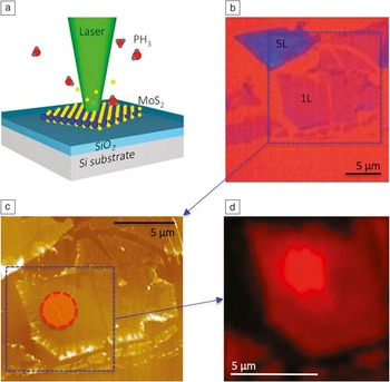
Two-dimensional TMDC layered materials with the formula MX2 (M = Mo, W; X = S, Se, Te) have direct bandgaps ranging from 1.5 to 2.0 eV, therefore, a visible range laser is an effective choice for processing. Laser-assisted phosphorus doping in ultrathin (monolayer and bilayer) TMDCs, including n-type MoS2 and p-type WSe2, was recently demonstrated using a 532-nm-wavelength laser, which is a versatile, air-stable, and tunable method, carried out by varying the duration and intensity of a focused laser irradiating in a phosphine environment to accomplish site-specific doping ( Figure 3 ). Reference Kim, Ko, Kim, Chen, Suh, Ryu, Wu, Meng, Suslu, Tongay, Wu and Grigoropoulos34 Extending the laser-doping method to emerging 2D layered materials will not only allow site-specific selectivity, but also prevent the redistribution of the impurity profile via a pulsed laser with short irradiation duration. As mentioned earlier, ultrafast lasers may provide a new pathway to TMDC layer doping through atomic-scale control of vacancy generation and the subsequent refilling with impurity atoms via non-thermal lattice disturbance processes. Reference Komsa, Kotakoski, Kurasch, Lehtinen, Kaiser and Krasheninnikov11
Laser-assisted doping of MoS2. (a) Schematic diagram of laser-assisted doping. Focused laser locally illuminated onto the MoS2 flakes (blue atoms, Mo; yellow atoms, S) located on a SiO2/Si substrate under diluted phosphine (PH3) dopant gas environment. The function of laser illumination is to create sulfur vacancies and simultaneously dissociate the dopant molecules in preparation for the subsequent doping process. (b) Optical image of as-prepared monolayer (1L) and five-layer (5L) MoS2 on a SiO2/Si substrate (blue color represents MoS2). (c) Atomic force microscope image of the (b) zoomed area. Its thickness is approximately 0.7 nm, in good agreement with the thickness of monolayer MoS2. The circle in (c) is the laser spot area in the laser doping. (d) Photoluminescence (PL) mapping of the zoomed area in (c) that clearly shows the PL intensity enhancement of the laser-assisted doped area. Reference Kim, Ko, Kim, Chen, Suh, Ryu, Wu, Meng, Suslu, Tongay, Wu and Grigoropoulos34

Further ultrafast laser processing of 2D layered materials and in situ diagnostics
Considering that engineering of imperfections or defects in 2D layered materials (e.g., vacancies, edges, dopants, adsorbates, or substrates) can play a critical role on the properties (e.g., electrical, optical, thermal, or magnetic) of 2D layered materials owing to their low dimensionality, atomic-scale subtractive and additive control over the 2D layered materials can be a powerful processing tool. To this end, optical near-field technology can be used to improve lateral processing resolution, as demonstrated at the nanoscale by various processing examples, Reference Ryu, Kim, Hwang and Grigoropoulos35–Reference Hwang, Ryu, Misra, Jeon and Grigoropoulos37 or laser-assisted atomic layer deposition or etching to achieve atomic thickness level control toward 2D layered heterostructure fabrication. Reference Grigoropoulos, Hwang and Chimmalgi36,Reference Ohtsu, Kobayashi, Ito and Lee38
For achieving high throughput and precision, various schemes have been proposed for scalable and programmable processing on the basis of multiple laser light confining elements in conjunction with in situ diagnostics and metrology. Reference Pan, Hwang, Ko, Clem, Frechet, Bauerle and Grigoropoulos39 Integrating in situ process monitoring tools, such as both optical far- and near-field laser illumination arrangements, into scanning and transmission electron microscopes will enable investigation of the fundamental interaction mechanisms of ultrafast lasers with 2D layered materials. Reference In, Ryu, Lee, Ahn, Zheng, Hwang and Grigoropoulos40–Reference Hwang, Xiang, Ryu, Dubon, Minor and Grigoropoulos42 Further, the structural modification signature measured by the imaging and analytical diagnostic functions of electron microscopes can be correlated with in situ measured optical spectroscopic signals (e.g., in situ Raman spectroscopy Reference Allen, Kim, Ryu, Ozdol, Grigoropoulos and Minor43,Reference Allen, Kim, Andresen, Grigoropoulos and Minor44 ).
Conclusion and outlook
Ultrafast lasers can drive a wide range of subtractive and additive processes for the patterning and functionalization of atomic layered materials. Mechanisms such as multiphoton absorption, minimized thermal effects, non-thermal interactions, as well as compatibility and integration with advanced diagnostics can be beneficial in this effort. Research at the fundamental level with the aid of in situ diagnostics tools is necessary to achieve atomic-scale manipulation. Furthermore, ultrafast lasers can be configured to scalable processing tools and therefore realize the next-generation high-performance portable, flexible, and wearable devices based on 2D materials.
Acknowledgments
Lawrence Livermore National Laboratory is operated by Lawrence Livermore National Security, LLC, for the US Department of Energy, National Nuclear Security Administration under Contract DE-AC52–07NA27344. E.K. acknowledges support to the Laser Thermal Laboratory at UC Berkeley by the National Science Foundation (NSF) under Grant No. EEC-1449305. The laser doping experiments were carried out at the Laser-Assisted Chemical Vapor Deposition setup in the University of California, Berkeley Marvell Nanolab. Analysis of the doped structures was conducted in collaboration with J. Wu’s team at University of California, Berkeley Materials Science & Engineering. D.H. acknowledges the support of Grant No. 14CTAP-C086566–01–000000 from Technology Advancement Research Program funded by the Ministry of Land, Infrastructure, and Transport of the Korean government, and also to the industry technology R&D program of MOTIE/KEIT No. 10050501. The authors thank Y.F. Lu at the University of Nebraska–Lincoln for contributing results on ultrafast laser direct writing of graphene patterns, supported by the NSF (CMMI 1265122), Nebraska Center for Energy Sciences Research, and the US Office of Naval Research (N0014-019-1-0943).

Jae-Hyuck Yoo is a postdoctoral research staff member at Lawrence Livermore National Laboratory. He earned his PhD degree in mechanical engineering from the University of California, Berkeley, in 2014. Yoo’s current research interests focus on laser-damage mechanisms of wide-bandgap semiconductors for transparent conducting films with high-laser-damage performance and laser-material-processing techniques with in situ diagnosis.

Eunpa Kim is a senior engineer at Samsung Electronics. Prior to this, he was a postdoctoral fellow at the University of California, Berkeley. He received his PhD degree in mechanical engineering from the University of California, Berkeley, in 2014. Kim’s research interests include micro-/nanoscale fabrication and nanometrology of low-dimensional semiconducting nanomaterial.

David J. Hwang is an assistant professor in the Department of Mechanical Engineering at The State University of New York at Stony Brook. He received a PhD degree in mechanical engineering from the University of California, Berkeley (UCB), in 2005. He was a postdoctoral researcher from 2005 to 2007 and a research scientist from 2008 to 2010 at UCB. He was a guest scientist of Lawrence Berkeley National Laboratory from 2007 to 2010. Hwang’s research interests focus on micro-/nanoscale heat transfer and laser-assisted materials processing and diagnostics for a wide range of applications.