Introduction
Discoveries of the mid-20th century have helped shape the character and quality of our modern technological landscape. The 1940s and 1950s brought remarkable breakthroughs in materials science ranging from the theory of dopants to the first imaging of individual atoms and identification of the double-helix structure of DNA. This era also produced the first transistor, the first silicon solar cell, and development of the first lasers. New discoveries about materials properties enabled new devices that in turn provided more insight into the fundamental nature of materials.
Around this time, a graduate student at the University of Tennessee—Rufus Ritchie—began researching the energy losses of electrons passing through metallic films. Ritchie was fascinated by then recent experiments indicating that the energy loss spectrum was characterized by several equally spaced sharp lines—implying that electrons lose their energy in integral multiples of some fundamental unit. The results were not consistent with a free-particle treatment, in which the motion of electrons in a metal is assumed to be independent of all other electrons. David Pines and David Bohm at Princeton suggested that the energy loss spectra might be due to collective oscillations of the electron plasma in the metal.Reference Bohm and Pines1, Reference Pines2 Ritchie coined this new elementary oscillation a “plasmon” and began to explore its energy and angle-dependent properties.Reference Ritchie3 By further investigating the effect of the film thickness, Ritchie accounted for depolarization effects near surfaces and provided the first analysis of “surface plasmons.”Reference Frank, Arakawa and Birkhoff4 His theoretical work laid the foundation for what is now the thriving field of plasmonics.Reference Barnes, Dereux and Ebbesen5–Reference Stockman8
As defined by Ritchie, surface plasmons are collective oscillations of conduction electrons at the interface between a conductor and non-conductor. Whether excited by electrons or photons, plasmons represent a “hybrid” electron-photon mode confined to a conductor; the electrons oscillate with an amplitude and phase reminiscent of light waves, but are bound to a conducting surface. Because of the dual electronic and photonic nature of surface plasmons, they are characterized by extremely high electric field intensities and extremely small mode wavelengths. Compared to electromagnetic waves in vacuum, plasmonic fields can be enhanced by more than two orders of magnitude.Reference Tanabe9 Further, their modal volumes can be reduced by more than two orders of magnitude.Reference Miyazaki and Kurokawa10 These two properties—extreme field enhancement and confinement—render plasmons a fascinating playground for photonics, allowing optical signals to be controlled on length scales comparable to electronic wavelengths.
Since their discovery in 1957, surface plasmons have been exploited in applications as diverse as single-molecule surface-enhanced Raman spectroscopy,Reference Fleischmann11–Reference Moskovits13 nanoscale optical modulators,Reference Stockman, Zheludev, Macdonald and Sa14, Reference Berini and De Leon15 high-efficiency solar cells,Reference Atwater and Polman16, Reference Polman and Atwater17 improved photocatalysts,Reference Linic, Christopher and Ingram18–Reference Novo, Funston and Mulvaney20 nanoscale lasers,Reference Hill, Oei, Smalbrugge, Zhu, De Vries, Van Veldhoven, Van Otten, Eijkemans, Turkiewicz, De Waardt, Geluk, Kwon, Lee, Notzel and Smit21–Reference Oulton, Sorger, Zentgraf, Ma, Gladden, Dai, Bartal and Zhang24 biological rulers,Reference Liu, Hentschel, Weiss, Alivisatos and Giessen25, Reference Sönnichsen, Reinhard, Liphardt and Alivisatos26 and electromagnetic metamaterials for invisibility and sub-diffraction-limited optical microscopy.Reference Shalaev27–Reference Shin and Fan31 The explosive growth of the field is reflected in the scientific literature: since 1990, the number of papers related to surface plasmons has nearly doubled every five years. Advances in nanofabrication and characterization have accelerated this growth. Techniques such as electron beam lithography and focused ion beam milling have allowed complex plasmonic architectures to be fabricated with nanometer-scale precision. In parallel, sophisticated chemical synthetic techniques have enabled “bottom-up” assembly of diverse plasmonic nanoparticle shapes, sizes, and morphologies. Breakthroughs in electron microscopy and spectroscopy, including aberration-corrected transmission electron microscopy and cathodoluminescence imaging as well as in photon scanning tunneling microscopy, have allowed characterization of electric and magnetic plasmonic fields with near atomic-scale resolution. The ability to create and characterize complex plasmonic structures provides a powerful yet precise handle of photons in the nanoworld.
As surface plasmons celebrate their 55th anniversary, this issue of MRS Bulletin highlights the progress and promise of plasmonics. Attention is given to breakthroughs following the May 2005 MRS Bulletin issue on “Synthesis and Plasmonic Properties of Nanostructures,”Reference Xia and Halas32 including
• Integrated plasmonic circuits for subwavelength optical communications and computation
• Plasmonic tweezers for light-controlled mechanical manipulation of nanoparticles and biomolecules
• Development of tools to image plasmonic fields with sub-5-nm resolution, using advanced electron microscopy, spectroscopy, and super-resolution microscopy
• The emergence of quantum plasmonics, where the quantum nature of light and/or electrons leads to properties unique from a classical description
• Loss compensation in plasmonic devices using novel materials such as transparent conducting oxides, transition metal nitrides, semiconductors, and graphene.
The discoveries, challenges, and prospects discussed in each article imply a thriving golden era and bright future for plasmonics.
Passive and active plasmonic devices
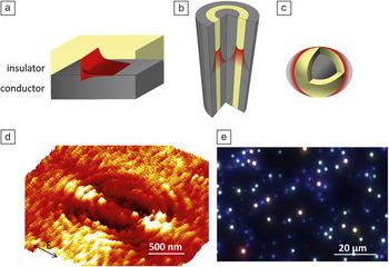
While surface plasmons were first identified on metallic films, there are a number of geometries that support surface plasmons. Figure 1 (a–c) illustrates three plasmonic structures that form the basis for many plasmonic devices, including a planar film, a coaxial pillar, and a nanoparticle. These structures highlight the key distinctions between propagating, localized, and hybrid plasmons and also provide a framework for understanding more complex plasmonic architectures.
Surface plasmons are supported at the interface between a conductor and an insulator in a variety of geometries, ranging from films to multilayers and nanoparticles. The intensity profile of plasmons, indicated by the red curves, is maximized at the conductor/insulator interface and decays away from the surface (a–c). This allows for high confinement of electromagnetic fields, as well as high field intensities. Plasmon propagation at the surface of an elliptical gold resonator, formed by patterning an elliptical groove in a gold film, is illustrated in (d), as imaged using a photosensitive resist and atomic force microscopy.Reference Dionne33 Dark-field microscopy can be used to image the plasmon resonances of ∼10–100 nm silver nanoparticles, as seen in (e).

A planar conducting film supports surface plasmons that propagate as transverse-magnetic waves along its interface with an insulator.Reference Economou115, Reference Kretschmann and Raether116 As seen in Figure 1a, electric fields are maximized at the conductor-insulator interface, but they decay evanescently in the perpendicular direction—usually within a few tens to hundreds of nanometers. Since the momentum of plasmons on planar films usually exceeds that of photons in free-space, a prism, grating, groove, or scatterer must be used to provide photons with sufficient momentum to excite surface plasmons. Figure 1d illustrates plasmon propagation along a single gold interface, excited using 514 nm light incident on an elliptical groove.Reference Dionne33 Here, a thin, electric-field-sensitive photoresist on the gold was used to record plasmonic fields as topographic changes that could later be imaged with atomic force microscopy. Outside of the groove, the plasmon decays within a few microns in the direction of propagation. Within the ellipse, the surface plasmon forms a standing wave that maps the allowed modes and foci of the ellipse. The ripples in the resist correspond to a surface plasmon wave with a wavelength of 438 nm—about 15% smaller than the wavelength of the incident light. Depending on the film material, thickness, and surrounding media, plasmon wavelengths can be tuned down to tens of nanometers, while propagation lengths can exceed millimeters. Their sensitivity to these parameters—particularly the index of the surrounding media—has rendered planar plasmonic architectures as efficient biological sensorsReference Anker, Hall, Nilam, Zhao and Van34 and optical modulators.Reference Pacifici, Lezec and Atwater35
In addition to propagation along a single conducting interface, plasmons can also propagate within narrow dielectric channels. For example, a shallow groove in a metallic film supports “channel” plasmon polariton modes that propagate along the dielectric region with minimal decay into the surrounding metal.Reference Bozhevolnyi, Volkov, Devaux, Laluet and Ebbesen36, Reference Gramotnev and Pile37 Similarly, metal-insulator-metal or semiconducting-insulator-metal multilayers can support “gap”Reference Dionne, Sweatlock, Atwater and Polman38–Reference Oulton, Sorger, Genov, Pile and Zhang40 or “hybrid”Reference Waele, Burgos, Polman and Atwater41 plasmon polariton modes. Akin to linear combinations of atomic orbitals, these modes resemble linear combinations of single-interface plasmonic modes. For example, Figure 1b illustrates a coaxial plasmonic geometry composed of a metal-insulator-metal multilayer structure with cylindrical symmetry.Reference Waele, Burgos, Polman and Atwater41, Reference Saleh and Dionne42 As with the single metallic interface geometry, plasmons in the coax propagate along the metal-dielectric interface, with maximum field intensities at the metal-dielectric boundary. However, unlike single interface plasmons, the field intensities within the dielectric channel can be much larger, and these gap plasmons propagate with a much higher degree of confinement. Interestingly, the metallic and semiconducting layers in multilayer plasmonic structures not only serve to confine plasmons, but can also double as electrical contacts. Such structures have been implemented as efficient electro-optic modulators,Reference Dionne, Diest, Sweatlock and Atwater43, Reference Cai, White and Brongersma44 as interconnects for short-range optical data transmission,Reference Dionne, Lezec and Atwater45 and also as gradient-index media (including negative index media).Reference Burgos, de Waele, Polman and Atwater46 Multilayer plasmonic resonators have also formed the basis for room-temperature nanoscale lasers, some capable of achieving thresholdless lasing.Reference Hill, Oei, Smalbrugge, Zhu, De Vries, Van Veldhoven, Van Otten, Eijkemans, Turkiewicz, De Waardt, Geluk, Kwon, Lee, Notzel and Smit21–Reference Oulton, Sorger, Zentgraf, Ma, Gladden, Dai, Bartal and Zhang24
As seen in Figure 1c, a conducting nanoparticle with dimensions much smaller than the wavelength of light exhibits a purely localized plasmon resonance, reminiscent of an electric dipole.Reference Kreibig and Vollmer117 Its scattering spectrum depends sensitively on the particle size, shape, charge, and the surrounding dielectric media. For example, Figure 1e illustrates a dark-field optical micrograph of silver nanoparticles of various sizes (10–100 nm); while smaller particles preferentially scatter toward the blue spectral regime, larger particles scatter preferentially toward the red. The strong local resonances supported by plasmon nanoparticles have been utilized in biological and catalytic sensing,Reference Novo, Funston and Mulvaney20, Reference Anker, Hall, Nilam, Zhao and Van34 as well as in “spasing”—surface plasmon amplification by stimulated emission of radiation.Reference Noginov, Zhu, Belgrave, Bakker, Shalaev, Narimanov, Stout, Herz, Suteewong and Wiesner47, Reference Stockman48 Such spasers represent the smallest surface plasmon lasers to date. Further, since nanoparticle extinction cross-sections are usually much larger than the physical particle size, plasmon nanoparticles serve as efficient receiving and transmitting “nanoantennas” for optical signals.Reference Alonso-González, Albella, Schnell, Chen, Huth, Garcia-Etxarri, Casanova, Golmar, Arzubiaga, Hueso, Aizpurua and Hillenbrand49–Reference Alù and Engheta52, Reference Nevet, Berkovitch, Hayat, Ginzburg, Ginzach, Sorias and Orenstein118 Most recently, plasmon nanoparticles have been implemented as novel photodetectors based on hot-electron injection into a semiconductorReference Knight, Sobhani, Nordlander and Halas53 and as optical rectifiers that convert optical fields into dc electrical power via resonant plasmon absorption.Reference Sheldon and Atwater54
The article by Sorger and colleagues in this issue discusses integration of such passive and active plasmonic components for on-chip plasmonics. Particular attention is given to plasmonic interconnects, plasmonic sources (such as lasers, spasers, and light-emitting diodes), modulators (including all-optical and electro-optical switches), and detectors based on planar, hybrid, or nanoparticle plasmon modes. Like photonic circuits, plasmonic circuits promise higher bandwidth, higher speed, lower latency, and reduced power consumption than electronic circuits.Reference Dionne, Sweatlock, Sheldon, Alivisatos and Atwater55 Plasmonic circuits also promise miniaturization of photonic circuits—with deeply subwavelength dimensions and dense component integration commensurate with electronic circuits. Such an integrated plasmonic technology could revolutionize the speed, size, cost, and power requirements of modern computational networks, provided key challenges such as loss and inter-device coupling can be addressed.
A strong hold on nano-objects: Plasmonic optical tweezers
Plasmonic components allow for precise sculpting of electromagnetic fields on deeply subwavelength scales. Beyond applications to optical communication and computation, this property is a key enabler for optical tweezing—the trapping and manipulation of objects using radiation pressure. Conventional optical tweezers rely on gradient forces within a diffraction-limited laser focus.Reference Ashkin, Dziedzic, Bjorkholm and Chu56 Their ability to manipulate small objects with light has enabled unprecedented opportunities in the biosciences. For example, optical tweezers have allowed for non-invasive manipulation of individual living cells,Reference Ashkin, Dziedzic and Yamane57 as well as a deeper understanding of molecular motors.Reference Bustamante, Bryant and Smith58 However, because optical trapping forces in the Rayleigh regime scale with the cube of the object radius,Reference Smith, Ashkin and Tomlinson59 conventional optical trapping of submicron-sized particles is challenging—requiring either an increase in the local field intensity or a strong reduction of the potential well width. Plasmonic tweezers address both requirements, enabling high local electromagnetic field intensities in subwavelength volumes.Reference Juan, Righini and Quidant60, Reference Grigorenko, Roberts, Dickinson and Zhang61 As described in the article by Quidant, plasmonic nanostructures can act as a “nanolens” capable of concentrating light beyond the capabilities of a microscope objective. Accordingly, plasmonic components allow nanoscale objects to be trapped and manipulated with much smaller optical powers than would be required with conventional optical tweezers.
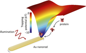
Plasmonic tweezers were first realized using a planar metallic film, as in Figure 1a. The largely increased electric field intensities at the metal-dielectric interface provided a nearly 40-fold enhancement in the trapping forces compared to conventional optical tweezers.Reference Volpe, Quidant, Badenes and Petrov62 More recently, plasmonic tweezers have been implemented with plasmonic nanoantennas, as shown in Figure 2. A single subwavelength Au nanorod produces plasmon hot spots (i.e., regions of strong electromagnetic fields) that result in an ∼10-k BT-deep potential well (where k B is Boltzmann’s constant, and T is the temperature).Reference Juan, Righini and Quidant60 The well depth and full-width-at-half-maximum can be tuned by varying the antenna geometry. For example, gap nanoantennas composed of two closely spaced metallic nanoparticles have been used to trap 200 nm polystyrene beads, living Escherichia coli bacteria, and 10 nm Au nanoparticles.Reference Righini, Ghenuche, Cherukulappurath, Myroshnychenko, García de Abajo and Quidant63, Reference Zhang, Huang, Santschi and Martin64 Plasmonic nanoantennas have also been used to rotate particles by rotation of the incident polarization.Reference Wang, Schonbrun, Steinvurzel and Crozier65
Plasmon nanoantennas, such as metallic nanorods, have been used as optical tweezers for trapping and manipulating nanoscale objects ranging from ∼10 nm particles to proteins. Their highly localized electromagnetic fields produce deep trapping potentials in subwavelength volumes.

Currently, research in plasmonic tweezers is aimed at trapping and manipulating much smaller particles, in the sub-10-nm regime. An important advance in this area has been the development of self-reconfigurable (or self-induced back action) traps; these plasmonic tweezer designs dynamically adjust the field intensity and the trap position to compensate for Brownian motion of the particle. To date, such plasmonic traps have enabled trapping of 20 nm polystyrene beads and large proteins (dimensions of ∼10 nm).Reference Chen, Juan, Li, Maes, Borghs, Van Dorpe and Quidant66, Reference Pang and Gordon67 More sophisticated optical plasmonic traps are likely to lead to trapping of single, sub-10-nm particles and proteinsReference Sainidou and García de Abajo68, Reference Yang, Liu, Oulton, Yin and Zhang69 and perhaps, ultimately, even single atoms.
Nanometer-scale imaging and characterization of plasmons
The fidelity with which plasmonic components can be used to manipulate optical signals relies in large part on our ability to characterize plasmonic fields. Two pivotal developments of the past decade have enabled characterization of plasmonic modes with sub-5-nm resolution: super-resolution microcopy and electron spectroscopy. While both tools are complementary to near-field optical techniques (which detect evanescent fields and provide a resolution of ∼15 nm), super-resolution microscopy and electron spectroscopy can provide insights into dynamic plasmon processes, often with the ability to resolve polarization and angle-dependent profiles.
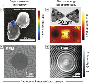
Super-resolution microscopy techniques—such as PALM (photoactivated localization microscopy) and STORM (stochastic optical reconstruction microscopy)—use the fluorescence signal from isolated emitters to achieve sub-diffraction-limited resolution. While the emission of a fluorophore is characterized by a Gaussian curve with a diffraction-limited full-width at half-maximum, the centroid of the emission defines the observed signal position. Provided no other emitters are nearby, this centroid position can be calculated to better than 5 nm—significantly better than the diffraction limit of light.Reference Gordon, Ha and Selvin70–Reference Thompson, Larson and Webb72 The article by Weber and Willets describes application of such super-resolution imaging techniques to mapping plasmonic hot spots and tracking the motion of single molecules near plasmonic nanostructures. For example, Figure 3a illustrates the surface-enhanced Raman scattering (SERS) spectral signal from a single R6G molecule near an Ag nanoparticle dimer.Reference Weber and Willets73, Reference Stranahan and Willets74 The SERS spatial intensity map—plotted via a color map—is overlayed onto a scanning electron micrograph of the dimer. Using super-resolution techniques, the molecule’s motion and SERS intensity can be tracked in real-time, providing insight into how molecules explore plasmonic hot spots. Complementarily, single-molecule fluorescence can be used to accurately map the near-fields of plasmonic structures with ∼5-nm resolution.Reference Cang, Labno, Lu, Yin, Liu, Gladden, Liu and Zhang75, Reference Wu, Liu, Sun and Zhang76
Advances in optical and electron microscopy allow plasmonic systems to be probed with nanometer-scale resolution. (a) Correlated super-resolution microscopy and electron microscopy of surface-enhanced Raman hot spots in a nanoparticle dimer.Reprinted with permission from Reference Reference Weber and Willets73. ©2011, American Chemical Society. (b) Correlated transmission electron microscopy and electron energy-loss spectroscopy (EELS) of a plasmonic mode in a silver nanoantenna. Adapted with permission from Reference Reference Koh, Fernández-Domínguez, McComb, Maier and Yang80. ©2011, American Chemical Society. The EELS map was acquired for electron energies of ∼1.5 eV (λ = 828 nm). (c–d) Correlated scanning electron microscopy (SEM) and cathodoluminescence (CL) spectroscopy of a silver plasmonic nanoresonator. Adapted with permission from Reference Reference Hofmann, Vesseur, Sweatlock, Lezec, Garcia de Abajo, Polman and Atwater86. ©2007, American Chemical Society. The CL map was acquired for photon energies of ∼1.9 eV (λ = 661 nm). SERS, surface-enhanced Raman scattering.

Electron-based techniques have also emerged as powerful probes of plasmonic modes. The article by Vesseur et al. discusses cathodoluminescence (CL) imaging spectroscopy and electron energy loss spectroscopy (EELS) to achieve near atomic-scale resolution of plasmonic fields. In both techniques, an electron incident on a nanostructure acts as a white-light or broadband point-source that excites plasmonic modes.Reference García de Abajo77 EELS measurements rely on detection of electrons transmitted through a plasmonic structure, similar to Ritchie’s first surface plasmon measurements; peaks in the energy loss spectrum correspond to excitation of surface and bulk plasmonic modes.Reference Ritchie3, Reference Batson78 Recent advances in monochromated and aberration-corrected transmission electron microscopy have allowed for unprecedented imaging (<0.3 nm resolution) and spectroscopy of plasmonic components, recently with ultrafast time resolution (see Figure 3b).Reference Nelayah, Kociak, Stephan, García de Abajo, Tence, Henrard, Taverna, Pastoriza-Santos, Liz-Marzan and Colliex79–Reference Scholl, Koh and Dionne82
In contrast, CL measurements rely on photons emitted by the excited modes upon radiative relaxation; these photons can then be detected in the far-field of a scanning electron microscope.Reference van Wijngaarden, Verhagen, Polman, Ross, Lezec and Atwater83, Reference Bashevoy, Jonsson, Krasavin, Zheludev, Chen and Stockman84 By scanning the electron source and the detector wavelength, full maps of plasmonic modes can be obtained across the visible and near-infrared spectrum. Recent advances in CL have also enabled reconstruction of angle- and polarization-dependent plasmon emission.Reference Coenen, Vesseur and Polman85 The resolution of CL imaging spectroscopy is limited only by the scanning electron microscope, with sub-5-nm accuracy readily obtained. For example, Figure 3c–d illustrates a scanning electron micrograph of a plasmonic ring resonator (a 2.6 micron Au disc surrounded by 15 concentric grooves) and its corresponding CL image, acquired by collecting photons of wavelength 661 nm.Reference Hofmann, Vesseur, Sweatlock, Lezec, Garcia de Abajo, Polman and Atwater86 A plasmonic standing wave with multiple antinodes (i.e., maxima) is clearly observed within the resonator. The image implies that plasmon resonances in CL are most efficiently excited at the antinodes of the electric field—indicating that the electron beam couples to plasmonic modes via the local density of optical states (LDOS).Reference Kuttge, Vesseur, Koenderink, Lezec, Atwater, García de Abajo and Polman87 Therefore, CL imaging spectroscopy can be used to map the photonic and plasmonic LDOS with nanometer-scale resolution. CL techniques can also be used to map plasmon dispersion, propagation, and emission profiles. To date, the technique has been applied to systems ranging from single metallic nanoparticles and nanowires to plasmonic whispering gallery cavities, metal-insulator-metal waveguide (MIM) nanoantennas, and plasmonic metamolecules.Reference Vesseur and Polman88–Reference Zhu, Ma, Zhang, Xu, Wu, Zhang, Han, Fu, Liao, Chen and Yu91
Electron beams can also induce forces, similar to plasmonic tweezers. The article by Vesseur et al. discusses new techniques to manipulate particles within an electron microscope, exploiting the interaction between plasmonic fields and the incoming electron. This “nanobilliards” approach has recently been used to move single, nanometer-scale Au nanoparticles in a transmission electron microscope.Reference Reyes-Coronado, Barrera, Batson, Echenique, Rivacoba and Aizpurua92, Reference Batson, Reyes-Coronado, Barrera, Rivacoba, Echenique and Aizpurua93 Both attractive and repulsive forces can be engineered, opening the door to complementary characterization and assembly of complex plasmonic nanostructures.
Toward quantum plasmonics
In recent years, the finesse with which plasmonic systems can be explored has entered the quantum realm. Here, properties such as entanglement, wave-particle duality, tunneling, and discretized energy levels emerge. For example, it was recently shown that two photons remain entangled upon conversion to plasmons, even though plasmons involve a macroscopic number of conduction electrons.Reference Altewischer, van Exter and Woerdman94–Reference Fasel, Robin, Moreno, Erni, Gisin and Zbinden96 In other words, plasmons behave as a single quantum entity. Related measurements demonstrated that plasmons can coherently exist at different times separated by much longer periods than the plasmon lifetime, due to the energy-time uncertainty principle.Reference Fasel, Robin, Moreno, Erni, Gisin and Zbinden96 Double-slit measurements and plasmon self-interference indicate that plasmons behave as waves.Reference Zia and Brongersma97, Reference Kolesov, Grotz, Balasubramanian, Stoehr, Nicolet, Hemmer, Jelezko and Wrachtrup98 But plasmons can also behave as particles, as evidenced by antibunching experiments of coupled Ag nanowire/diamond NV-center emitters.Reference Kolesov, Grotz, Balasubramanian, Stoehr, Nicolet, Hemmer, Jelezko and Wrachtrup98
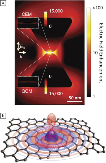
The article by Jacob explores the exotic properties of quantum plasmons, evident when either the particle nature of photons or the wave nature of electrons emerges. Attention is first given to quantum light—the interaction of plasmonic systems with non-classical light sources (i.e., single photon emitters.) Based on the broadband tunability of the LDOS and Purcell factor, plasmons can significantly increase the efficiency of single photon sources. Such an effect has been observed in metallic structures and is predicted to be even stronger in novel plasmonic systems based on graphene.Reference Akimov, Mukherjee, Yu, Chang, Zibrov, Hemmer, Park and Lukin99–Reference Koppens, Chang and García de Abajo101 The article also discusses quantum matter—where the wave nature of matter manifests itself in localized plasmon resonances. For example, surface plasmons in nanoparticles less than approximately 5 nm in diameter exhibit quantum behavior reflecting the discretized, quantum nature of conduction electron transitions.Reference Scholl, Koh and Dionne82 Similarly, closely spaced metal nanoparticles are predicted to exhibit quantum tunneling that shifts the plasmon resonance from a classical description, as illustrated in Figure 4a.Reference Esteban, Borisov, Nordlander and Aizpurua102 Quantum effects can also emerge in metamaterials—artificially engineered materials with vastly tunable electric permittivities and magnetic permeabilities. Metamaterials with strong dielectric anisotropy exhibit singularities in the density of states and topological transitions (i.e., abrupt changes in the isofrequency surface of allowed wave vectors).Reference Cortes, Newman, Molesky and Jacob103, Reference Krishnamoorthy, Jacob, Narimanov, Kretzschmar and Menon104 Such properties increase the electromagnetic states available to emitters while simultaneously channeling single-photon emission into subwavelength dimensions.
New plasmonic materials and properties may enable an entirely new class of plasmonic devices. (a) In the quantum realm, plasmons exhibit properties such as tunneling, entanglement, and wave-particle duality. For example, plasmon modes in a bow-tie nanoantenna will tunnel across the antenna gap. This quantum phenomenon changes the local field profile—as calculated with a quantum corrected model (QCM)—compared to a classical electromagnetic model (CEM). Reprinted with permission from Reference Reference Esteban, Borisov, Nordlander and Aizpurua102. ©2011, Nature Publishing Group. (b) Doped semiconducting films, nanoparticles, and graphene may out-perform noble metals as plasmonic materials and metamaterials. These materials support relatively low-loss, electrically tunable surface plasmons in the visible and infrared and can enable strong light-matter interactions. Reprinted with permission from Reference Reference Koppens, Chang and García de Abajo101. ©2011, American Chemical Society. In this figure, a dipole source is used to excite very short wavelength surface plasmons on a graphene film. k, wave vector.

While many features of quantum plasmonic systems remain unknown, numerous applications to subnanometer-scale photonics can be envisaged. For example, quantum plasmon transitions and tunneling are expected to have a significant impact on single molecule spectroscopy and biochemical sensing. Quantum plasmonic systems could increase spontaneous emission rates beyond stimulated emission, potentially enabling auto-fluorescence of normally weak emitters and ultrafast modulation of nano-sized light-emitting diodes.Reference Yablonovitch105 Further, by increasing the interaction of single photons with matter, quantum plasmonic systems could enable efficient single-photon sources, detectors, and transistors—potentially revolutionizing future quantum optical networks.
Novel plasmonic materials: Overcoming loss
Perhaps the biggest challenge facing plasmonics is loss. While metals provide the requisite negative electric permittivity for subwavelength confinement, they are also characterized by a significant imaginary component of the permittivity. This large absorption hinders long-range plasmon propagation in waveguides, challenges the development of gain-based components such as surface plasmon lasers and transistors, and serves as a significant impediment to metamaterial applications, such as electromagnetic cloaks and superlenses. In recent years, several clever experiments have addressed plasmon loss. For example, plasmon amplification and lasing have been observed in planar, cylindrical, and stripe waveguides, as well as in spasing nanoparticles.Reference Berini and De Leon15 Moreover, gain has been introduced into resonator-based metamaterials to achieve low-loss and even active negative index media.Reference Xiao, Drachev, Kildishev, Ni, Chettiar, Yuan and Shalaev106 While the results are encouraging, considerable pump power or operation well below room temperature is usually required. The field of plasmonics would benefit tremendously from new materials systems that could allow simultaneous subwavelength optical confinement and loss mitigation.Reference Khurgin and Sun107, Reference Tassin, Koschny, Kafesaki and Soukoulis108
The article by Khurgin and Boltasseva tackles this grand challenge of plasmonics, first identifying the fundamental cause of plasmonic loss and then proposing mechanisms to overcome it. By definition, surface plasmons represent coupling of an electromagnetic field to the kinetic motion of free carriers. Plasmon absorption (i.e., loss of kinetic energy) occurs through two mechanisms: (1) transitions from occupied to unoccupied states in the main s-p conduction band (intraband transitions) or (2) transitions from occupied states in the d-band to unoccupied states in the s-p band (interband transitions). The primary way to reduce absorption is to reduce the density of states available for scattering. This consideration motivates the use of highly doped semiconductors as alternatives to noble metals.
Recently, transparent conducting oxides and transition metal nitrides have received considerable attention as low-loss plasmonic materials. For example, indium tin oxide and gallium-doped zinc oxide exhibit metallic properties for wavelengths longer than 1.3 microns, while aluminum-doped zinc oxide (AZO) becomes metallic past 1.8 microns. At technologically relevant near-infrared frequencies, the losses of AZO are about four times smaller than those of Ag.Reference Naik, Kim and Boltasseva109 Materials such as titanium nitride (TiN) and zirconium nitride offer visible-frequency conductivity, becoming metallic for wavelengths longer than 500 nm. Compared to silver and gold, TiN offers comparable performance for plasmonic applications and significantly improved performance for metamaterial applications.Reference Naik, Schroeder, Ni, Kildishev, Sands and Boltasseva110 Semiconducting quantum dots have also been explored as alternatives to noble metal nanoparticles. Localized surface plasmons have been observed in semiconducting quantum dots of copper sulphide, tungsten oxide, and indium tin oxide.Reference Manthiram and Alivisatos111–Reference Garcia, Buonsanti, Runnerstrom, Mendelsberg, Llordes, Anders, Richardson and Milliron113 Further into the infrared, graphene has been shown to support extremely short-wavelength plasmons, with wavelengths of ∼200 nm achievable at free-space wavelengths of 10 microns (see Figure 4b).Reference Cortes, Newman, Molesky and Jacob103, Reference Fei, Rodin, Andreev, Bao, McLeod, Wagner, Zhang, Zhao, Thiemens, Dominguez, Fogler, Castro Neto, Lau, Keilmann and Basov114, Reference Chen, Badioli, Alonso-González, Thongrattanasiri, Huth, Osmond, Spasenović, Centeno, Pesquera, Godignon, Zurutuza Elorza, Camara, García de Abajo, Hillenbrand and Koppens119 Unlike noble metals, the permittivity of these doped semiconductors and graphene can be vastly tuned by electrical or chemical modulation. The low loss and optical tunability of these materials could be a transformative technology, with applications ranging from integrated plasmonics to metamaterials and plasmon photovoltaics.
Outlook
Plasmonics has achieved astounding progress over the past 55 years. Born of a simple question about energy loss peaks in metallic films, plasmonics has now entered diverse application areas ranging from optoelectronics to photovoltaics, catalysis, chemistry, biology, medicine, quantum optics, and even art. A search on Google Scholar returns over 300,000 scholarly articles related to “plasmons,” 18,000 of which were published since 2011. The field now has its own journal, its own Gordon conference, and has fueled several start-up companies. The articles selected for this issue represent just a small but exciting cross-section of plasmonics research. They highlight important foundational work and a vision for the future: Integrated plasmonic circuits may one day transmit petabytes of data; non-invasive gene repair might be enabled by plasmonic tweezers; plasmonic forces might enable atom-by-atom assembly; advanced plasmonic microscopies may permit subnanometer-scale structural probes; and quantum plasmonic phenomena may lead to advanced quantum communication, computation, and cryptography. Undoubtedly, new discoveries about plasmonic properties will enable new devices and, in turn, provide more insight into the fundamental nature of plasmonic modes. But to paraphrase Niels Bohr, every sentence uttered must be understood not as an affirmation, but as a question. Just as plasmonics began with one spark of curiosity, we hope the articles in this issue of MRS Bulletin will inspire many more questions to come.
Acknowledgments
We are immensely grateful to all of the authors who contributed an article to this issue of MRS Bulletin. Special thanks to Amr Saleh and Sassan Sheikholeslami for providing assistance with figures; and to Jonathan Scholl, Ashwin Atre, Aitzol Garcia-Etxarri, Andrea Baldi, Hadiseh Alaeian, Brian Baum, Justin Briggs, Vivian Ferry, Dennis Callahan, Matt Sheldon, Diane Wu, and Mark Brongersma for insightful discussions. J.A.D. and H.A.A acknowledge the AFOSR, NSF, DOE, ARO, and GCEP for their generous support of research on plasmonic materials and metamaterials.