Introduction
The principle of printed electronics involves the use of printing processes to apply liquid inks made from electrically conducting, semi-conducting, and insulating materials in several superimposed layers on plastic films.Reference Rost1 The printing is carried out according to a specified design in order to create electrical components and circuits. These are used in applications such as radio frequency identification (RFID) tags. Therefore, fast and high-volume roll-to-roll production processes allow for the manufacturing of low-cost RFID tags for new mass applications.Reference Rost and Clemens2
This technology is also used for other applications such as display elements, solar cells, and complex systems known as smart objects. The term “printed smart objects” refers to a combination of various printed electronic components, such as input elements in terms of switches, displays, energy sources such as batteries and solar cells, sensors, and control electronics. Combinations of these individual components enable a wide range of new applications. Thus, for example, by combining a printed battery with a logic circuit, an input element and a display, it is possible to construct disposable sensors, games, or information displays.Reference Ludwig and Rost3 The possibility to print new functional materials on large and flexible substrates is opening up many markets for new applications in areas where conventional (inorganic) electronics have limited or no access.
The main advantage of printed electronics is that all the necessary components for integrated circuits and RFID tags can be printed within the same layer structure. Therefore, the production of all components for a RFID tag, for example, can be realized on a flexible plastic substrate using the roll-to-roll principle and requires only a few printing steps. In order to develop a roll to roll process for printed electronics successfully, many different requirements have to be met, especially with respect to material, process, design, and testing properties. All materials must have adequate functionality, stability, and long-term availability at high quantity and low price. A suitable printing process requires a high production speed and must also be possible at temperatures well-below 120°C and with short drying times below 30 seconds. Furthermore, only non-toxic and non-explosive materials and solvents can be used in these processes.Reference Rost and Mildner4
Conductive transparent films
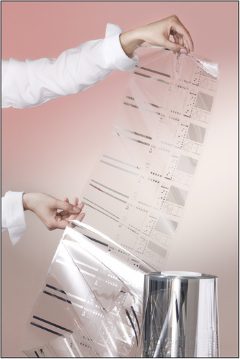
An example for the potential of printed electronics is the development of a printed transparent conductor utilizing a metallic grid by PolyIC GmbH & Co. KG. Figure 1 shows a photograph of the conductive and highly transparent PolyTC film.
Novel conductive and highly transparent films: PolyTC.

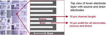
These printed grids were enabled through the printing process developed for RFID tags, in which many organic field-effect transistors with high functionality are required. High functionality, for instance, can be achieved with very high resolution, meaning a very small structure size of the lower electrode (source and drain electrodes, see Figure 2). Over the last few years, PolyIC has succeeded in developing a new production process for these electrodes. The new process offers the possibility to produce metal structures in terms of a grid or mesh with a very high resolution by a large-scale roll-to-roll operation. These printed metallic meshes can also be used as transparent conductive films, having a specific sheet resistance and transparency that can be individually engineered for the target application.
High-resolution patterns on plastic films; top view of lower electrode layer with source and drain electrodes.

Besides PolyIC, a number of other companies, such as Dai Nippon Printing, Fujifilm, Gunze, and 3M, are also active in the area of transparent conductive films using metal grids as a conductive material. Details about product properties can be found on the appropriate websites.
Substrate
For a number of other applications beside RFID, such as electrical window heating, displays, and electrodes for organic photovoltaics, both flexibility and transparency of the substrate are needed along with electrically conductive coatings. The great advantage is that in contrast to glass, flexible substrates can be applied in continuous production processes, such as roll-to-roll printing. So, in the past few years, thin conductive layers deposited on plastic films, especially on polyethylene terephthalate (PET), have been described.Reference Geng, Kim, So, Lee, Chang and Lee5, Reference Saran, Parikh, Suh, Muñoz, Kolla and Manohar6 PET film is suitable for printed electronics applications, as it offers a number of interesting features:
• Thin
• Flexible
• Suitable for 3D applications
• Exhibits a smooth surface
• Wettable by “electronic inks” (i.e., solutions of functional materials in organic solvents)
• Printable
• Available in heat-stabilized versions
• Commercially available in many different thicknesses
• Cost effective.
Besides PET, recently, thin polycarbonate films have also been reported as a substrate material for custom car interior design (i.e., decorative panels, planar or shaped touch keys, and switch covers). Due to its special thermal behavior for these applications, polycarbonate film can be applied by means of film insert molding.Reference Kuenzel and Pophusen7
Conductive layers
Generally, sufficient conductivity of functional layers on plastic films can be achieved through the use of pure metals or other chemical compounds. Layers of transparent conductive films can be made of noble (and thus relatively stable) metals such as gold, silver or copper, non-stoichiometric compounds derived from tin-, zinc-, and indium oxide (e.g., ITO), fluorine-doped metal oxides, and aluminum-doped zinc oxides. A widely used compound nowadays is the aforementioned ITO, which can be deposited onto glass or plastic films by different methods such as vacuum evaporation,Reference George and Menon8 sputtering,Reference Kerkache, Layadi, Dogheche and Renniens9 ion plating,Reference Huber and Pulker10 and chemical vapor deposition (CVD).Reference Maki, Komiya and Suzuki11 Finally, the generated thin conductive layer has to be treated by means of a chemical etching process in order to accomplish the desired conductive grid and/or conductive pattern. Komai et al.Reference Komai, Hotta and Moriyama12 describes a different approach for metal patterning on plastic foils using light-curable resins.
The most attractive method for generation of conductive grids on glass or a flexible plastic is the straightforward way (i.e., direct printing of the desired structure). Using silver pastes and nanoparticle inks, metallic patterns with a resolution down to 30 microns can be achieved by means of screen printing technology.Reference Jablonski, Mastropietro and Wargo13 While there are various attempts to use other inorganic materials such as carbon nanotubes (CNTs),Reference Saran, Parikh, Suh, Muñoz, Kolla and Manohar14 many companies are focusing on the development of new conductive polymers as printable alternatives to ITO coatings.
Polymers are generally known as non-conductive materials. However, there is a special class of polymers, referred to as intrinsically conductive polymers, whose conductivity lies between that of semiconductors and metals, in the range of 102 to 103 S/cm. A well-known example of an intrinsic conducting polymer with a certain transparency is the PEDOT/PSS (poly(3,4-ethylenedioxythiophene)/polystyrene sulfonate) system. Although PEDOT/PSS has already been successfully used as electrode material in simple devices, such as organic field-effect transistors,Reference Rost, Ficker, Sanchez Alonso, Leenders and McCulloch15 there is still room for improvement of its conductivity, at least for more complex applications, where almost metallic conductivity is needed. For photovoltaic devices, underlying metallic grids as electrical supports for PEDOT/PSS electrodes have been described.Reference Aernouts, Vanlaeke, Geens, Poortmans, Heremans, Borghs, Mertens, Andriessen and Leenders16 These grids were fabricated by means of the so-called diffusion transfer reversal process, which is a very important two-sheet photographic technique.Reference Van Hunsel, Coppens, Deprez, Odeurs and Vandenbergh17 Meanwhile, conductive formulations based on PEDOT/PSS are employed in different fields, such as antistatic coatings, capacitors, thick-film electroluminescence, and many more electronic devices.18
The production process
By producing high-resolution structures at the micrometer scale on thin and flexible PET films (the typical resolution is 10 μm), not only sufficient conductivity but also sufficient layer transparency can be achieved. Figure 2 shows high-resolution patterns on plastic films realized in PolyIC’s production process. Typically, for conductive features to be invisible, it has been empirically found that a contrast of less than 1% at conductive/insulating boundaries, or features less than about 20 microns in dimension, are necessary.Reference Mackey19 Therefore, the conductive grid of PolyIC is transparent because the 10 μm structures appear invisible to the human eye. An additional advantage of PolyIC’s approach is that conductivity and transparency of the grid can be tailored by adjusting the area occupancy ratio of the conductive material (width and density of the conductive structures per square meter of PET film).
Here, pure metals, such as silver or copper, are deposited onto PET films by means of a fast roll-to-roll process. Subject to the application, the metal patterns can be applied over the total film length and width or as an individual layout pattern. It should be noted that an appropriate choice of the grid pattern can prevent any anisotropy in conductivity, if desired. On the other hand, conductive shapes without the need for transparency (i.e., highly conductive tracks as electrical wiring) can be designed as well. In the case of such tracks, the metal lines are broader than the fine grid fingers while exhibiting the same metal layer thickness, which is generally in a range between 30 to 80 nm.
The metallic grids described previously can be made from noble and therefore stable metals (e.g., silver and copper) that are known for their resistivity against humidity, different chemicals, and moderate heat. When the PolyTC rolls are ready for further processing, one only has to take great care to avoid any contact between the metallic grid and human fingers, as fingerprints could be the possible starting point for metal degradation. Obviously, nanometer-thin metal layers are susceptible to salts and grease that are constituents of human finger sweat.
However, for most target applications, such as displays and touch sensors, a transparent protective layer is deposited directly onto the metal grid after the actual production process (i.e., before being used by the customer). Such a layer can be laid down on the grid either by laminating a very thin transparent plastic sheet or by direct printing and subsequent drying of transparent ink. The latter method has the great advantage that the protection layer can be deposited only where needed—with the contact pads remaining uncovered. Once deposited, this additional layer acts as an effective seal that provides the desired environmental stability.
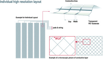
In the case of PolyTC, the functional layer is effective with only 5% coverage of the carrier substrate (PET) and exhibits up to 95% transparency while maintaining sufficient conductivity.Reference Fix, Knobloch, Ullmann and Woerle20 This is exactly what is needed for a number of applications, such as displays, touch sensors, and ultrathin heating elements. In Figure 3, a layout pattern for a transparent, conductive coating is shown as a representative example.
Conductive areas with additional pads and wiring as individual layout. All areas are printed with a metallic grid, whereas the structure sizes (width and gap) are minimum 10 μm, and larger sizes are possible, depending on the individual application. Additionally, not only a metallic grid, covering the overall area, but also a patterned grid is possible, reflecting the specific needs for different applications (e.g., need for patterned areas in the case of touch sensors). PET, polyethylene terephthalate.

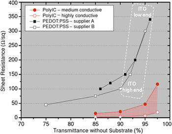
As mentioned, the applications, in principle, can be accomplished by means of conductive structures made from ITO. However, it should be considered that beside the material itself, the processing, both deposition and patterning of ITO, are time-consuming, tricky, and expensive. In particular, with respect to the scarcity of indium resources, the development of new technologies for transparent, conductive materials on plastic films is the focus of numerous research and development activities. Compared to these material systems, the new PolyTC technology offers advantages with respect to transparency and conductivity (Figure 4). As already noted, PolyTC conductive structures can be printed at a minimum resolution of only 10 microns. It is interesting that the metallic structures of that size do not need to be transparent themselves, as the necessary light transmission is achieved by a high-resolution structuring that the human eye is unable to resolve. In other words, the structures are too fine to get distinguished.
Comparison of different conductive and transparent materials—the red hatched area reflects the sheet resistance range that is possible with a metallic PolyTC grid. Sheet resistance and transparency of the grid can be tailored by adjusting the area occupancy ratio or the thickness of the conductive material.

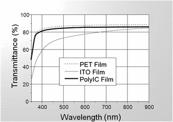
In fact, the conductive structure occupies only a small fraction of the whole area (<10%), allowing for the use of light-impermeable but highly conductive materials such as silver or copper. Through careful adjustment of the process parameters, sheet resistance values of 0.4 to 1 Ω/sq can be achieved depending on the process parameters that are used. Thus, the conductivity of the transparent area can also be individually designed to that of the typical values of ITO films. In addition, consistently high transparency can be achieved over a wide wavelength range and is therefore another advantage of this new technology.
Figure 5 shows the wavelength-independent transparency of PolyTC compared to the substrate itself and commercially available ITO-coated film. Compared to conventional ITO films, the conductive, transparent structures of PolyTC films offer advantages such as:
• Possibility of customer-specific, individualized layouts
• Cost-effective patterning processes
• High transparency over a wide wavelength range (400–800 nm)
• Customer-specific conductivity and surface resistivity
• Use of thin, lightweight, flexible PET substrates
• High volume products through the use of a roll-to-roll mass production process.
Transmittance of PolyTC films compared with indium tin oxide films. ITO, indium tin oxide; PET, polyethylene terephthalate.

Conclusion
For the strongly emerging display and touch sensor markets, new technologies are needed to meet the requirements of a continually growing demand for transparent conductive films. In addition, the development of alternative technologies to indium tin oxide (ITO) is also driven by requirements such as cost reduction and scarcity of indium resources. Obviously, cost-efficient roll-to-roll printing of inks made from functional materials seems to be an interesting approach.
The new PolyTC technology from PolyIC offers the possibility to produce transparent conductive films at high volumes and low cost by the use of a roll-to-roll mass production process. Additional advantages include customized layouts, high transparency, and high conductivity. Thus, the PolyTC technology for transparent, conductive layers may be considered an attractive alternative to ITO films.