

Introduction
UWB technology has attracted hot discussion since Federal Communications Commission (FCC) permitted 3.1–10.6 GHz for ultra-wideband (UWB) applications in 2002 [1]. Especially, UWB microstrip antennas have been paid more attention for their attractive features of low profile, compact volume, and easy manufacture [Reference Naghar, Falcone, Alejos, Aghzout and Alvarez2]. UWB systems work in a complex electromagnetic environment, which may cause latent electromagnetic interference to them, like WiMAX (3.3–3.7 GHz), WLAN (5.15–5.35, 5.725–5.825 GHz), and X-band (7.9–8.4 GHz). Meanwhile, multipath fading effect is also a challenge to UWB applications. To address the first issue, an effective approach is to design band-notched function without adding additional filter devices. As for multipath fading problem, multiple-input-multiple-output (MIMO) technology is taken as a good way since it can significantly improve system performances, such as capacity and multipath fading [Reference Kaiser, Feng and Dimitrov3].
In the past decades, many reports about multiple notched bands (NBs) for UWB systems have been discussed. In [Reference Bakariya, Dwari and Sarkar4], three round-shaped slots are etched on the radiator to notch WiMAX, lower WLAN, and upper WLAN. A pair of rectangular split-ring resonator is located beside the feeding line to filter 7.9–8.4 GHz X-band [Reference Sarkar, Srivastava and Saurav5]. In [Reference Ebadzadeh, Nourinia and Ghobadi6], symmetric step-shaped slits are etched to suppress 4 GHz C-band and 5.5 GHz WLAN. Ref. [Reference Karmakar, Ghatak, Banerjee and Poddar7] used Hilbert curve slot to obtain dual-NBs.
Recently, numerous studies about decoupling technique for MIMO antennas have been reported [Reference Bilal, Saleem, Shafique and Khan8–Reference Gogosh, Shafique, Saleem, Usman and Faiz16]. In [Reference Bilal, Saleem, Shafique and Khan8], a 50.5 mm × 30 mm UWB-MIMO antenna was presented. By introducing a T-shaped and sine-curve hybrid decoupling structure, port isolation of <−20 dB was obtained. Using a mushroom-type electronics band-gap, the MIMO antenna in [Reference Kumar9] provides isolation of −15 dB, but it only covers the frequency band from 3.8 to 7.8 GHz (−10 dB impedance bandwidth). In [Reference Chandel and Gautam10], covering UWB from 2.9 to 20 GHz, a compact size of 18 mm × 36 mm slot MIMO-UWB antenna was designed. With a T-shaped stub, isolation of <−20 dB was realized. Metal strip is used to achieve good isolation of better than −20 dB in ref. [Reference Li, Chu, Li and Xia11]. In [Reference Huang, Liu, Zhang and Gong12], without extra decoupling structures, low mutual coupling of −20 dB is easily reached by placing two identical monopole antennas vertically. Neutralization lines were applied in [Reference Zhang and Pedersen13] to obtain −22 dB port isolation, but only 3.1–5 GHz band was covered. Operating from 1.8 to 13 GHz band, the antenna in ref. [Reference Kumar, Krishna and Kushwaha14] used a TH-like stub to get isolation of better than −20 dB. With a tree-like decoupling element, isolation in [Reference Zhang, Ying, Xiong and He15] was <−16 dB. A novel H-type decoupling structure was proposed in [Reference Gogosh, Shafique, Saleem, Usman and Faiz16] to achieve −20 dB isolation. However, the antenna had a big size of 48 mm × 80 mm.
In the paper, a miniaturized UWB-MIMO antenna with four band-notched characteristics was proposed. Based on half-cutting method [Reference Gao and Zhang17], the antenna occupies 22 mm × 28 mm, and operates from 3 to 11 GHz except four rejected bands (3.25–3.6, 5.05–5.48, 5.6–6, and 7.8–8.4 GHz). An inverted L-like meander slot, two inverted L-shaped slots, and a C-shaped stub are inserted to filter WiMAX, lower WLAN, upper WLAN, and X-band. With a T-like stub, low frequency of impedance bandwidth is greatly improved. Meanwhile, mutual coupling is also enhanced effectively and port isolation of −20 dB is reached. There are scarce literatures about four notched-band UWB-MIMO antennas; and more importantly, it is very compact, which is smaller than some other UWB-MIMO antennas [Reference Bilal, Saleem, Shafique and Khan8–Reference Gogosh, Shafique, Saleem, Usman and Faiz16], even smaller than some UWB antennas [Reference Bakariya, Dwari and Sarkar4, Reference Sarkar, Srivastava and Saurav5, Reference Karmakar, Ghatak, Banerjee and Poddar7].
Antenna design
Configurations
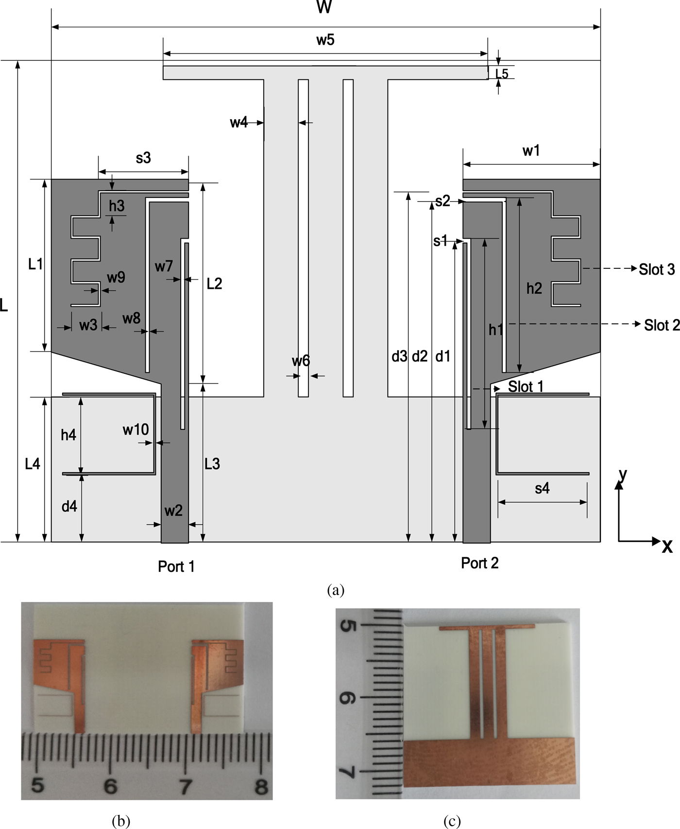
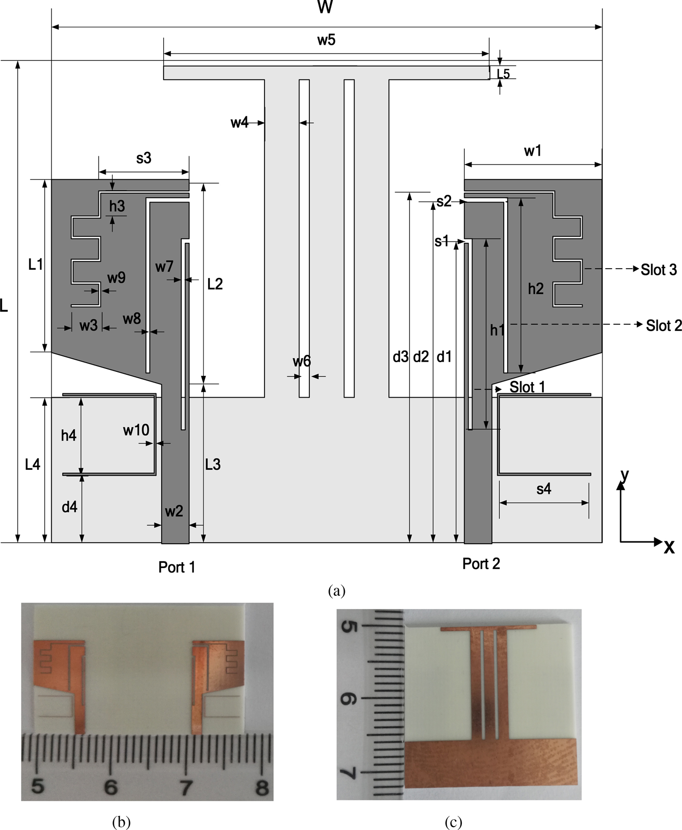
Figure 1 shows geometry and photo of the fabricated antenna. Final optimum antenna is printed on a 22 mm × 28 mm × 0.8 mm Rogers RO4003C substrate (dielectric constant of 3.38, loss tangent of 0.0027). The UWB-MIMO system comprises two similar radiation elements, which are fed by two 50 Ω microstrip feeding lines, respectively. Each radiation element consists of a rectangular radiator with a beveled edge, which helps to get wider impedance bandwidth. On the back side of the antenna, there are a partial ground plane and a T-like stub, which are extruding from the middle of the ground plane. By inserting two inverted L-shaped slots (denoted as Slot 1 and Slot 2, respectively), an inverted L-like meander slot (denoted as Slot 3), and a C-shaped stub, four NBs are created to filter 3.4 GHz WiMAX, 5.3 GHz lower WLAN, 5.8 GHz upper WLAN, and 8 GHz X-band.
(a) Geometry of proposed antenna and (b) front view (c) back view.
Antenna miniaturization
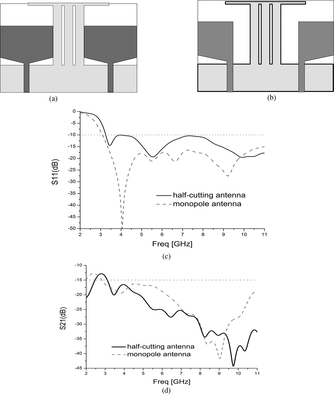
The prototype of monopole UWB-MIMO antenna and half-cutting monopole antenna is shown in Figs 2(a) and 2(b), respectively. Simulation results in Figs 2(c) and 2(d) are carried out by CST Microwave Studio. From Fig. 2(c), the monopole antenna, with a size of 22 mm × 34 mm, covers the UWB frequency band. Based on half-cutting method, half-cutting monopole antenna is reduced to 22 mm × 28 mm, which is nearly 22% smaller than the former. Importantly, it also covers the UWB frequency band and has better port isolation.
Prototype of antennas and simulation results of S-parameters: (a) monopole antenna, (b) half-cutting monopole antenna, (c) simulated S 11, (d) simulated S 21.

Effect of T-like stub
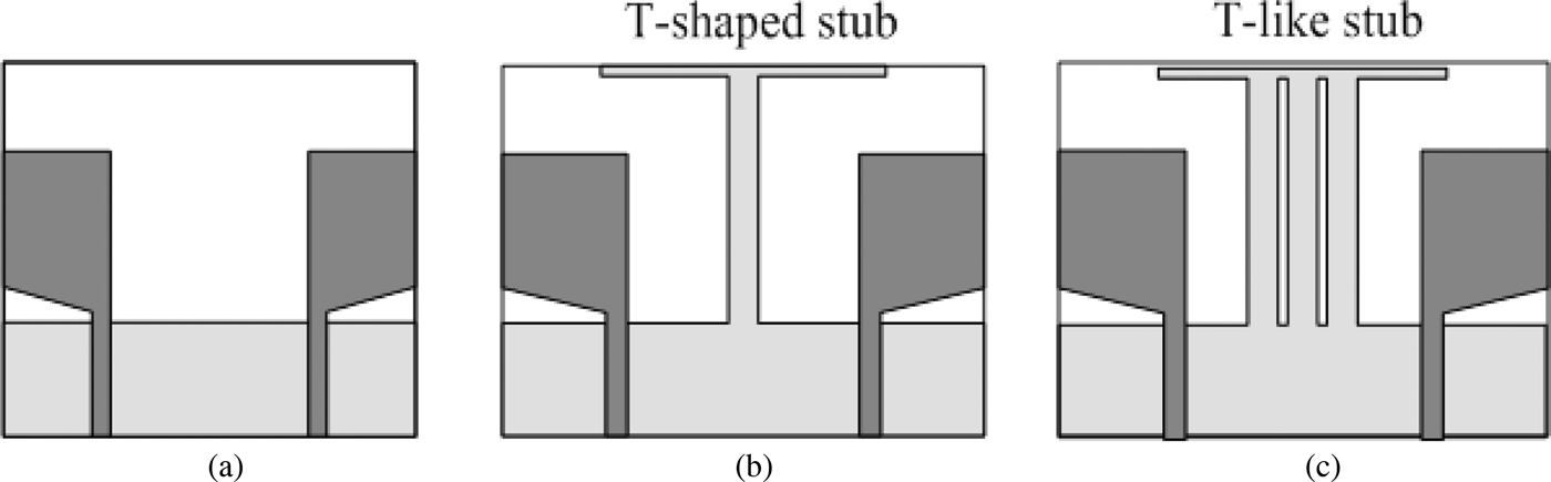
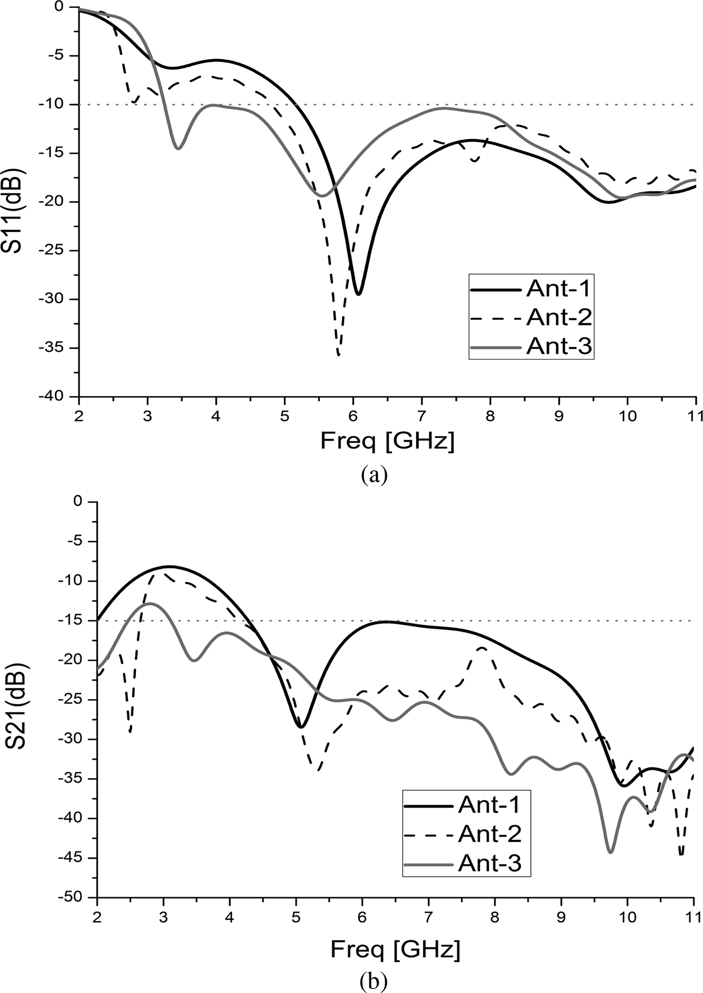
Figure 3 shows the design process of the ground plane. There is only a partial ground plane in Fig. 3(a). Then a T-shaped stub is added in Fig. 3(b). In Fig. 3(c), two symmetrical metal branches are placed beside the T-shaped stub. Figure 4 compares the effects of S parameters for the above three antennas that are named as Ant-1, Ant-2, and Ant-3. Since port 1 and port 2 are symmetry, only S 11 and S 21 are analyzed.
Different evolution of the ground plane: (a) Ant-1, (b) Ant-2, and (c) Ant-3.

Comparisons of S-parameters for Ant-1, Ant-2, and Ant-3.

From Fig. 4(a), the −10 dB impedance matching (S 11) below 5.4 GHz is poor for Ant-1. After adopting a T-shaped stub, impedance bandwidth is somewhat improved for Ant-2, and it is clearly improved at low frequency with the T-like stub for Ant-3. In Fig. 4(b), at the low-frequency band, the value of S 21 is above −15 dB for Ant-1. With the help of T-shaped stub, good improvements are made at the high frequency-band for Ant-2. Obviously, mutual coupling is effectively reduced with the T-like stub at low frequency for Ant-3, which can be taken as a reflector. Thus, the T-like stub plays an important role in impedance bandwidth and mutual coupling.
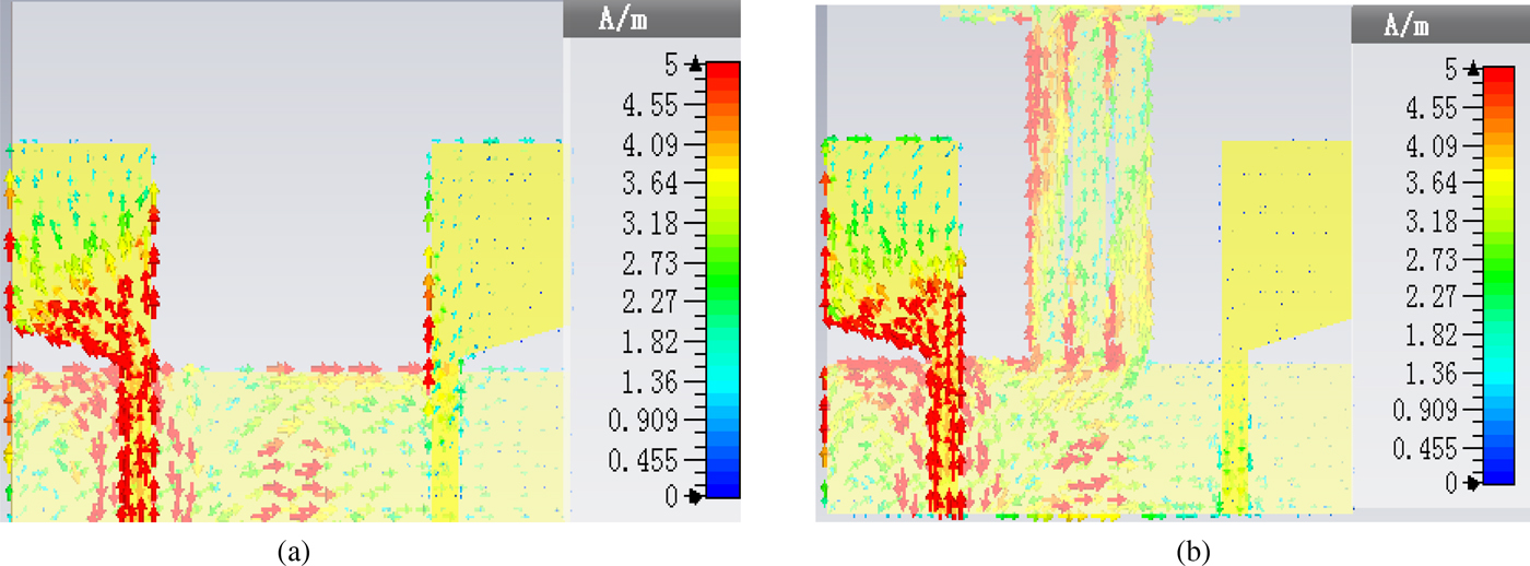
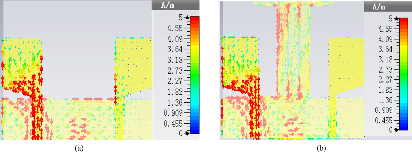
Figure 5 exhibits current density distributions at 4.5 GHz with and without T-like stub when port 1 is excited. From Fig. 5(a), a lot of electric current flows to port 2 via the ground. However, with the stub, as shown in Fig. 5(b), a large part of current is stopped from flowing to port 2, and port isolation is greatly improved.
Current density distributions at 4.5 GHz (a) without T-like stub, (b) with T-like stub.
Effect of slots and C-shaped stub
To achieve desired NBs, the length of resonator structures is set to half-guided wavelength or quarter-guided wavelength λ g, and
 $$\lambda _g = \displaystyle{c \over {\,f_c\sqrt {{\rm} \varepsilon _{eff}{\rm}}}}, $$
where c denotes light speed, f c denotes central frequency of the rejected bands, and εeff = (εr + 1)/2 is the effective dielectric constant.
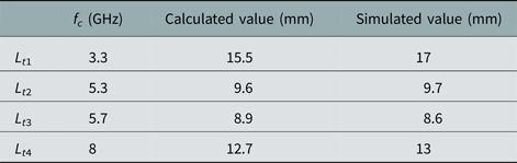
In the design, for Slot 1, Slot 2, and Slot 3, total length (L t1, L t2, and L t3) is set to a quarter of corresponding guided wavelength, and total length of C-shaped stub L t4 is a half-guided wavelength. Table 1 lists calculated and simulated values. By comparison, the two are very close, validating the design methods.
Comparison of calculated and simulated total length

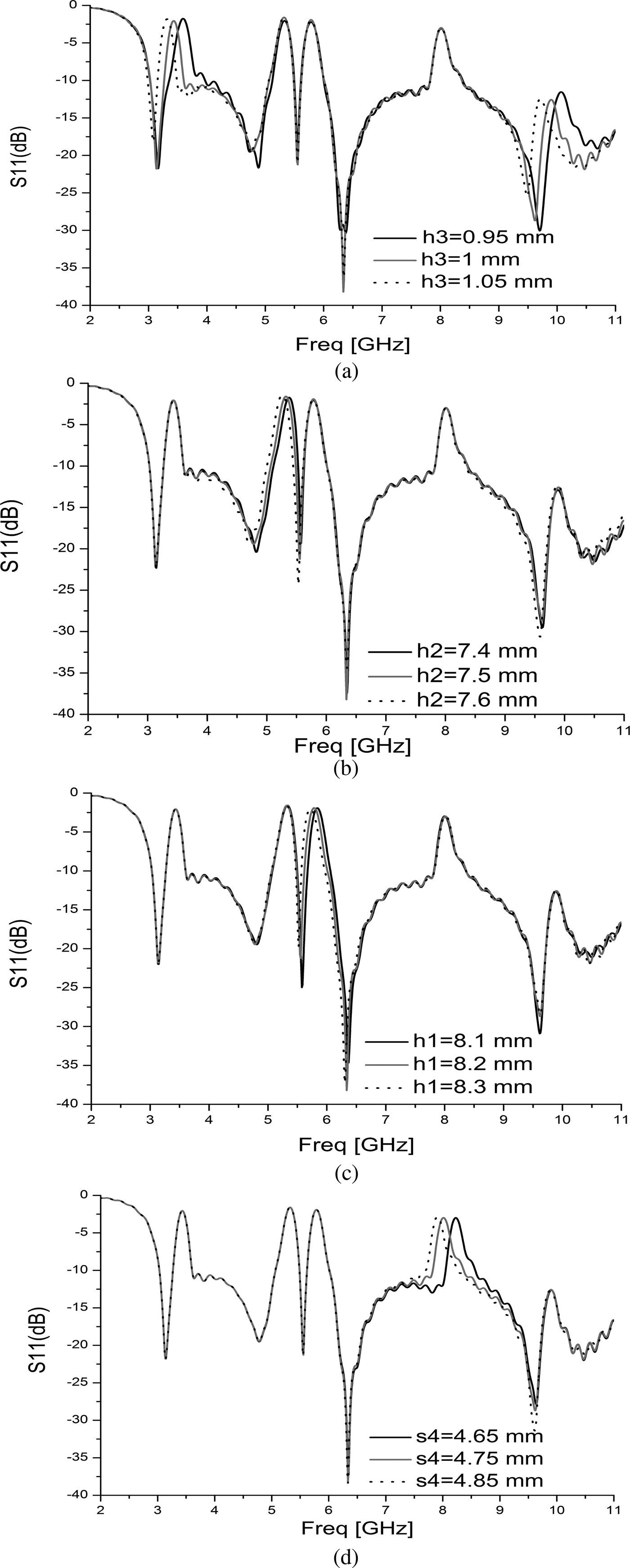
Next, four parameters are selected to observe their effect on S 11. When one parameter is changed, other parameters remain the same. Figure 6(a) describes the effect of h3 on S 11. Increasing h3 from 0.95 to 1.05 mm, the first NB shifts from 3.5 to 3.3 GHz, which can be verified by equation (1). So Slot 3 determines 3.25–3.6 GHz NB. In Figs 6(b) and 6(c), when h2 and h1 are increased respectively, the second NB and the third NB both move slightly to the left. From Fig. 6(d), length of the C-shaped stub is varied from 4.65 to 4.85 mm, the fourth NB moves from 8.2 to 7.8 GHz. Obviously, when one NB was controlled, the other NBs are almost unaffected. So each NB can be adjusted separately.
Simulated S 11: (a) effects of h3, (b) effects of h2, (c) effects of h1, (d) effects of s4.

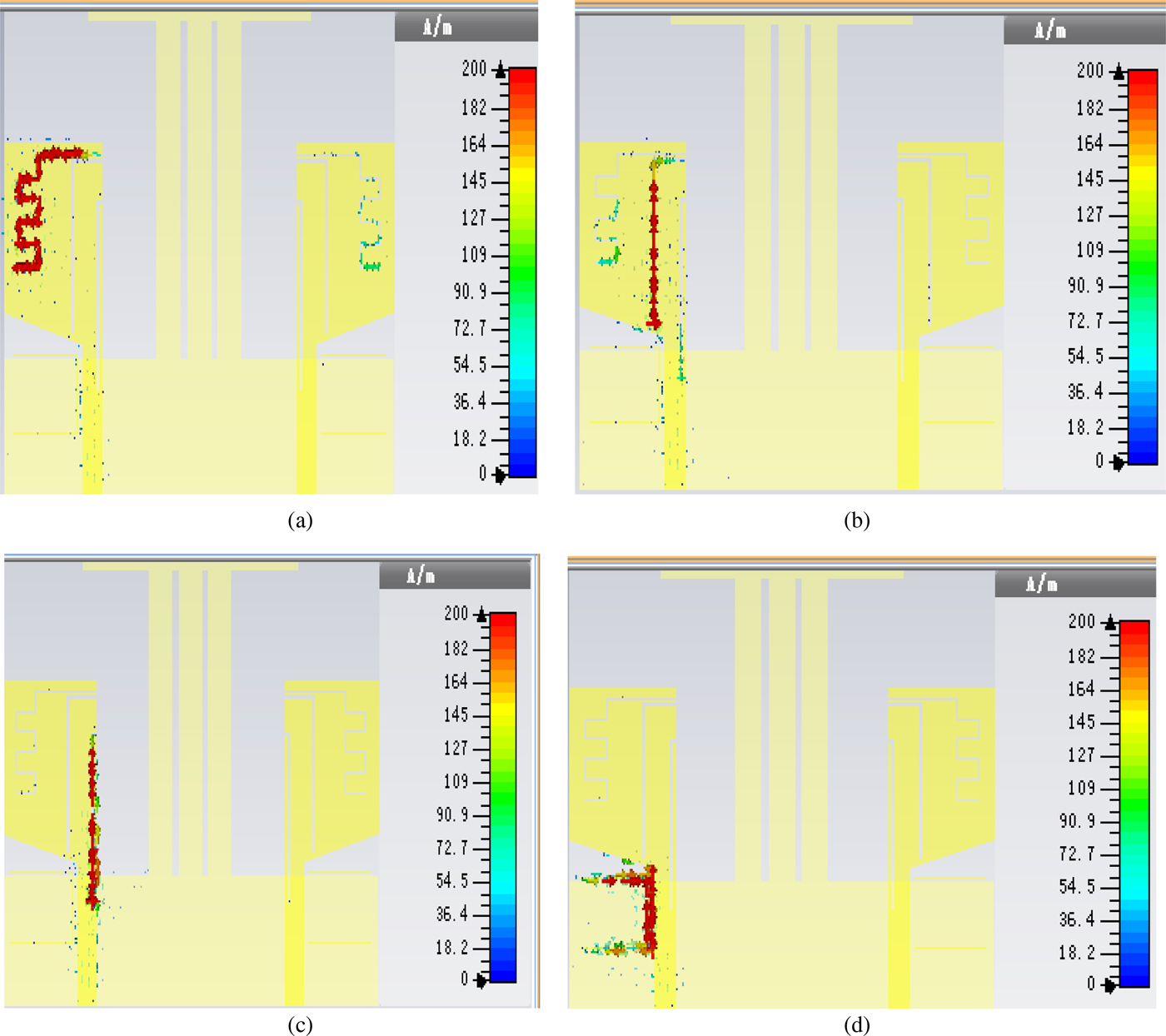
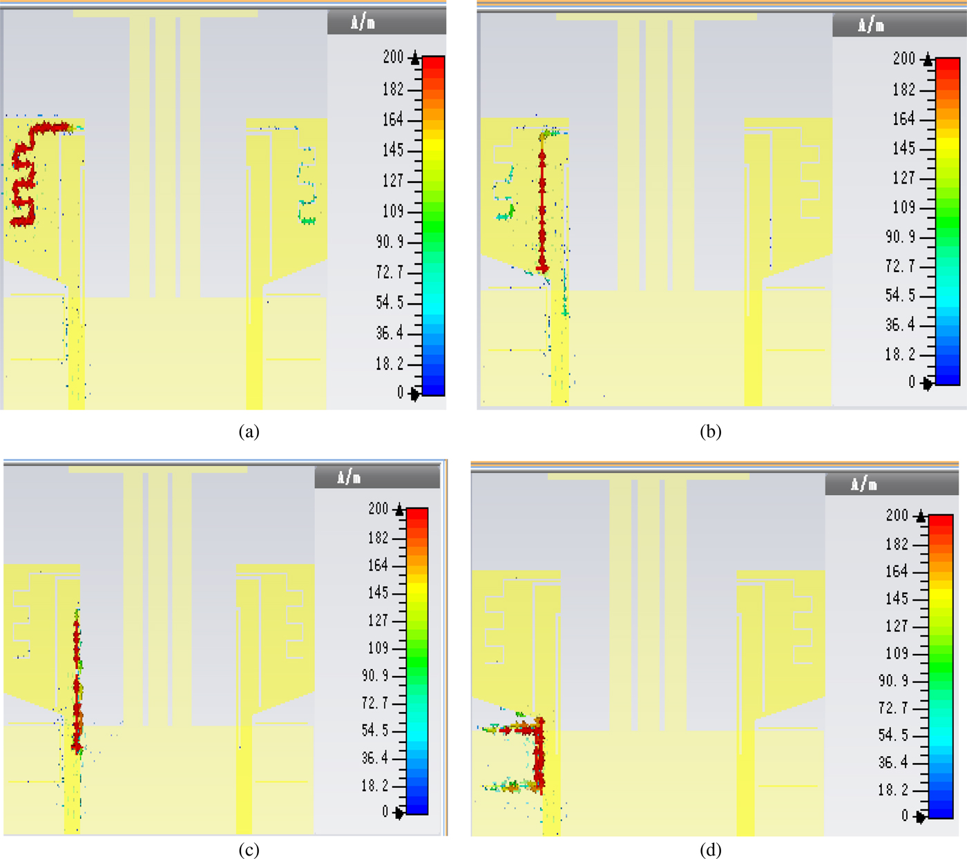
To better understand the formation mechanism of rejected bands, surface current distributions on proposed antenna at 3.4, 5.3, 5.8 and 8 GHz are shown in Fig. 7. From Fig. 7, strongest electric current mainly concentrates around corresponding resonator structure separately; signal propagation is stopped and energy cannot be transmitted by the antenna. Then four NBs are generated.
Surface current distributions when port 1 is excited: (a) 3.4 GHz, (b) 5.3 GHz, (c) 5.8 GHz, (d) 8 GHz.
Results and discussions
All the simulations are carried out using CST Microwave Studio. The final optimum antenna parameters are set as follows (Unit: mm):
W = 28, L = 22, L1 = 7.6, L2 = 9, L3 = 7, L4 = 6.4, L5 = 0.6, w1 = 7, w2 = 1.4, w3 = 1.5, w4 = 1.7, w5 = 16, w6 = 0.5, w7 = 0.2, w8 = 0.2, w9 = 0.1, w10 = 0.1, s1 = 0.4, s2 = 2.2, s3 = 4.5, s4 = 4.75, h1 = 8.2, h2 = 7.5, h3 = 1, h4 = 3.5, d1 = 13.2, d2 = 15, d3 = 15.4, d4 = 3.
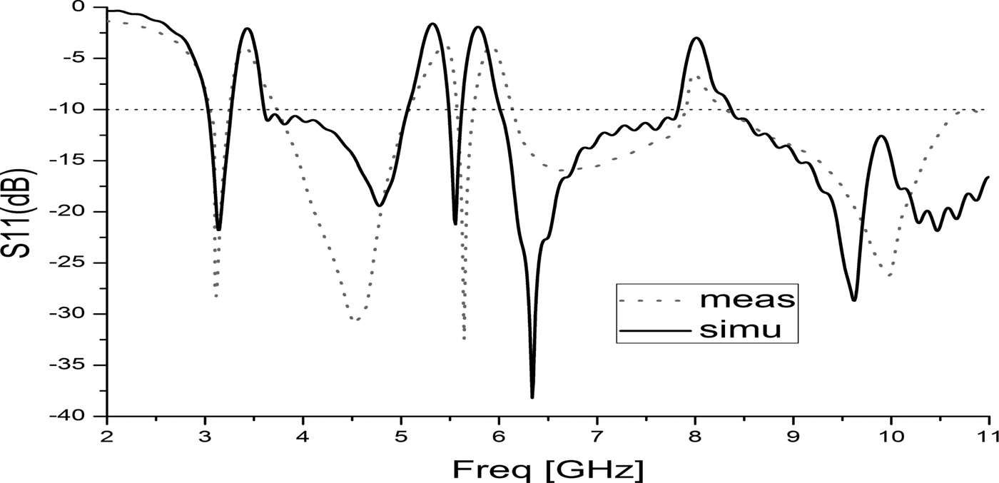
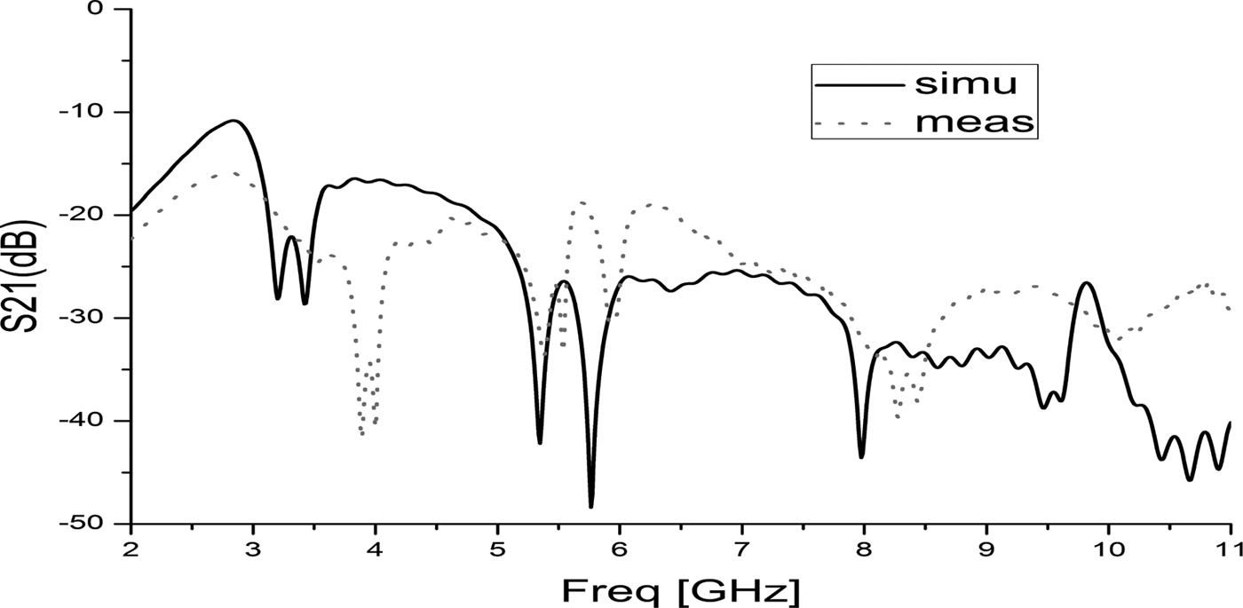
To verify the design concept, the antenna was fabricated and measured. The S-parameters of the proposed antenna were measured with Agilent E8362B network analyzer. Due to consistency of two ports, only S 11 and S 21 are discussed. Figure 8 shows the measured and simulated S 11. The −10 dB impedance bandwidth (S 11<−10 dB) extends from 3 to 11 GHz, which covers 3.1–10.6 GHz UWB band, while four rejected bands are observed at 3.25–3.6 GHz for blocking WiMAX, 5.05–5.48 GHz for lower WLAN, 5.6–6 GHz for upper WLAN, and 7.8–8.4 GHz for X-band. Figure 9 shows that the measured S 21 is smaller than −20 dB in the whole UWB band. This indicates that the proposed antenna not only meets UWB band but also can be applied for MIMO applications.
Simulated and measured S 11 of the proposed antenna.

Simulated and measured S 21 of the proposed antenna.

The results of simulations and measurements are basically in good accordance with each other in Figs 8 and 9, but some deviations exist. In Fig. 8, the measured S 11 curve moves slightly right, especially at the high-frequency band; and in Fig. 9, at the low-frequency band, the measurement S 21 is a little lower than simulation, but higher at the upper frequency band. These deviations may be caused by manufacturing errors and welding of SMA connector.
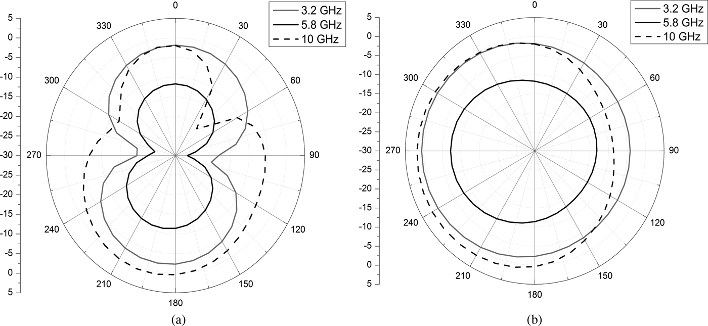
Figure 10 plots normalized far-field radiation patterns about y–z plane (E-plane) and x–z plane (H-plane) for port 1 at 3.2, 5.8, and 10 GHz. It can be observed that at notched frequency 5.8 GHz, received energy is relatively weak. However, at other frequency bands, the antenna behaves nearly as an omnidirectional radiation pattern in the H-plane and has a property of a dipole in the E-plane.
Far-field radiation patterns for port 1.

To further evaluate MIMO diversity characteristic, the envelope correlation coefficient (ECC) is studied. For two-port MIMO systems, ECC can be calculated by [Reference Blanch, Romen and Corbella18]:
 $$\rho _e = \displaystyle{{{\left\vert {S_{11}^\ast S_{12} + S_{21}^\ast S_{22}} \right\vert}^2} \over {(1 - {\left\vert {S_{11}} \right\vert}^2 - {\left\vert {S_{21}} \right\vert}^2)(1 - {\left\vert {S_{22}} \right\vert}^2 - {\left\vert {S_{12}} \right\vert}^2)}}$$
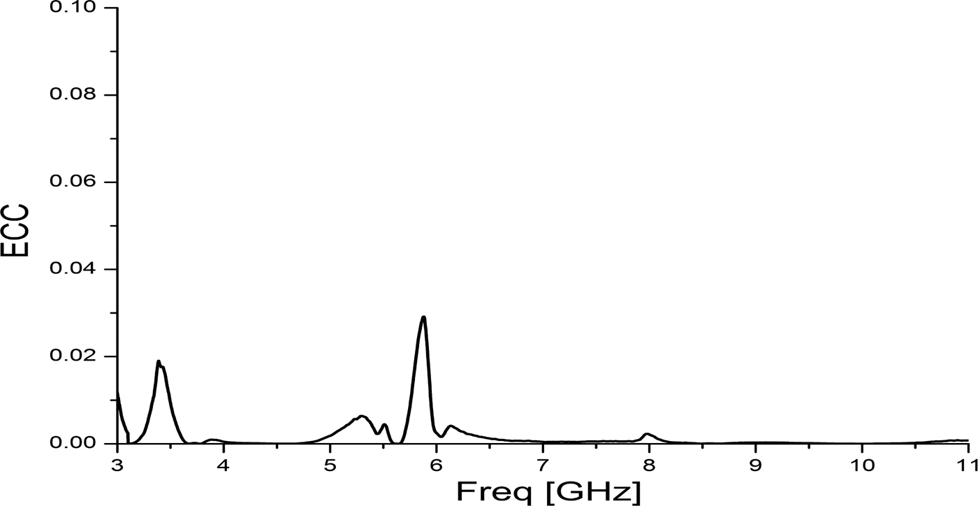
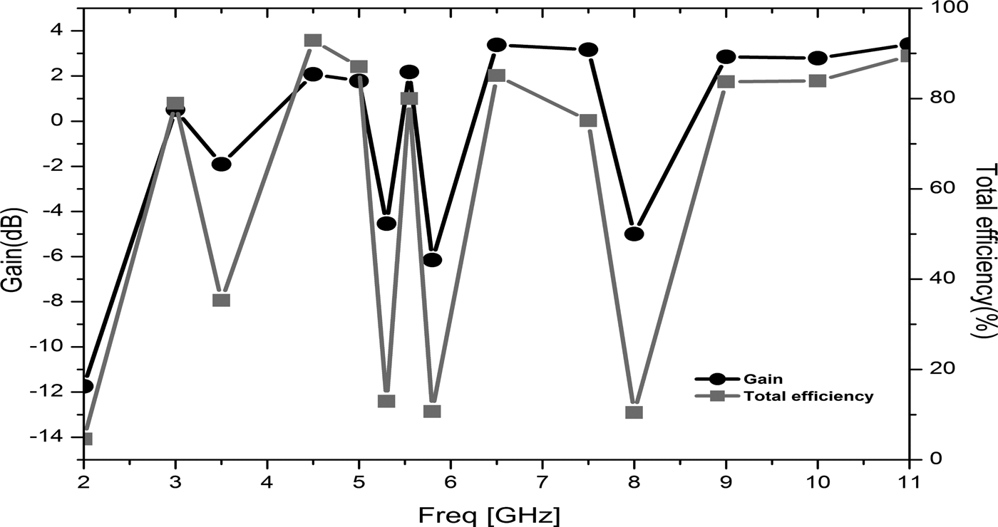
For symmetry of port 1 and port 2, S 11 = S 22, S 12 = S 21. Figure 11 illustrates that the ECC are below 0.03 across the 3.1–10.6 GHz UWB band. Figure 12 plots antenna gain and total efficiency when port 1 is excited. Except the four NBs, the gain varies gently and total efficiency is above 70% in the whole UWB band.
Measured ECC of the proposed antenna.

Antenna gain and total efficiency.

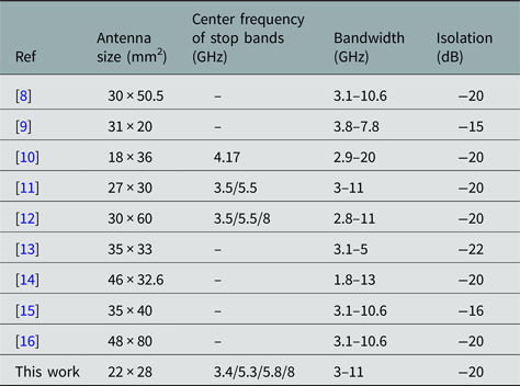
In the final, Table 2 compares the difference between the antenna and other two-port UWB-MIMO systems. The antennas [Reference Bilal, Saleem, Shafique and Khan8–Reference Gogosh, Shafique, Saleem, Usman and Faiz16] provide no more than triple NBs. Refs [Reference Bilal, Saleem, Shafique and Khan8, Reference Kumar9, Reference Zhang and Pedersen13–Reference Gogosh, Shafique, Saleem, Usman and Faiz16] render no filtering function, [Reference Chandel and Gautam10] notches 4.17 GHz C-band, [Reference Li, Chu, Li and Xia11] can suppress 3.5 GHz WiMAX and 5.5 GHz WLAN. Ref [Reference Huang, Liu, Zhang and Gong12] blocks WiMAX, WLAN, and X-band. It can be found that the proposed antenna not only provides quad-NB function, but also has the smallest size.
Comparisons of the antenna and other two-port UWB-MIMO systems

Conclusion
With quad-NB characteristics, a very compact UWB-MIMO antenna has been proposed. By inserting an inverted L-like meander slot, the first NB of 3.4 GHz is produced. With two inverted L-shaped slots, the second NB of 5.5 GHz and the third NB of 5.8 GHz are created. Using a C-shaped stub, the fourth NB of 8 GHz is obtained. With half-cutting method, size of the antenna is reduced to 22 mm × 28 mm. The results indicate that the system covers 3–11 GHz while filtering out 3.25–3.6 GHz WiMAX, 5.05–5.48 GHz lower WLAN, 5.6–6 GHz upper WLAN, and 7.8–8.4 GHz X-band. With a T-like stub on the ground, high isolation of better than −20 dB is easily achieved. Furthermore, ECC of less than 0.03 and good radiation patterns make it suitable for UWB systems.
Acknowledgements
The authors are grateful for the technical help provided by the electromagnetic microwave laboratory of Hua Zhong Normal University.
 Ling Wu received the B.S. degree in Huazhong Normal University, Wuhan, China, in 2004, and received the M.S. degree in Huazhong Normal University in 2007. Currently, she is a lecturer in Wuchang University of Technology, Wuhan, China. At the same time she is pursuing Ph.D. from Huazhong Normal University. Her main research includes microstrip-fed antenna design and signal processing.
 Yingqing Xia received the M.S. degree in Huazhong Normal University, Wuhan, China, in 1997 and received Ph.D. in Huazhong Normal University in 2003. From 2006 to 2007, he engaged in postdoctoral research in the University of Oxford. Presently he is a professor in Huazhong Normal University. He is interested in microwave circuits, embedded software and hardware systems, and applications.
 Xia Cao was born in HuBei, China. She received the B.S. degree in Huazhong Normal University, Wuhan, China, in 2004, and received the M.S. degree in Shantou University, Shantou, China, in 2008. Currently, she is a lecturer in Luojia College Wuhan University, Wuhan, China. At the same time, she is pursuing Ph.D. in Huazhong Normal University. Her main research includes communication engineering and embedded systems.
 Zhengtao Xu received the B.S. degree in ShanDong University of Technologe, Zibo, China, in 2011. Currently, he is pursuing M.S. from Huazhong Normal University, Wuhan, China. His main research includes software development and signal processing.