Introduction
Using paper as a substrate for electronics can be advantageous for environmental and economic reasons. One prerequisite is, however, additive and environmentally friendly manufacturing processes using non-toxic and recyclable structures, that can be incinerated or biodegraded without unnecessary harm. A candidate that fulfills such type of criterion is organic electronics.[Reference Allwood, Ashby, Gutowski and Worrell1, Reference Irimia-vladu, Głowacki, Voss, Bauer and Sariciftci2] The cornerstone of organic electronics is the organic transistor. However, large area manufacturing of organic transistors on well-behaved flexible substrates, such as e.g., polyester films (PET) has been proven challenging to say the least. The use of ion-modulated gate dielectrics for fabricating low-voltage transistors is very promising, due to the high capacitance of the electrolyte[Reference Sandberg, Bäcklund, Österbacka and Stubb3–Reference Koskela, Kilpelä, Björklund and Österbacka7] and also that it is less sensitive to manufacturing on rough substrates.[Reference Kaihovirta, Tobjörk, Mäkelä and Österbacka8] The problem with ion-conducting dielectrics is that there is always the possibility that ions from the electrolyte cause either reduction or oxidization of the semiconductor during operation, slowing down the switching time and operational speed of the transistor. This may avoided by using a polyanion to hinder anion penetration into the semiconductor.[Reference Herlogsson, Noh, Zhao, Crispin, Sirringhaus and Berggren9]
Paper as a substrate brings even more difficulties since the paper surface is both rough and absorptive. If the semiconductor layer is absorbed into the paper, the thickness, non-uniformity, and also the cost associated with manufacturing is increased. A thick semiconductor layer will result in slow switching due to the diffusive nature of the electrochemical process.[Reference Lee, Kaake, Cho, Zhu, Lodge and Frisbie10] Furthermore, the chemical composition of paper and polar molecules/groups present in the paper can and will affect the semiconductor layer in top-gate geometries, causing an extrinsic shunt resistance in the semiconductor at the paper surface. Moreover, the absorbent nature of the porous paper also causes problems with the semiconductor wetting metal electrodes. Owing to capillary forces, the semiconductor tends to absorb into the paper completely during the drying, leading to poor interfacial contact between the metal and semiconductor. Here we propose a method to solve the problem with the semiconductor absorption into the paper and speeding up the transistors by making extremely thin semiconductor layers utilizing spontaneous vertical phase separation. This entails mixing the semiconductor with a biodegradable polymer insulator. Owing to the favorable surface energies and kinetics involved in the process the insulator will adhere to the substrate and the semiconductor will form a thin layer on top of the insulator. As a result the semiconductor is not in contact with the paper surface and can be made very thin leading to faster switching transistors. We demonstrate that electronic circuits can easily be manufactured directly on the rough paper substrates, and that the operating frequency of the manufactured ring oscillators in a lateral gate configuration is greatly increased.
We use a method that relies on spontaneous phase separation to achieve a thin semiconductor layer.[Reference Qiu, Lim, Wang, Lee, Hwang and Cho11] We chose poly(L-lactic acid) (PLLA)[Reference Inkinen, Hakkarainen, Albertsson and Södergård12] [Fig. 1(b)] due to its biodegradability[Reference Asai, Komatsu, Shirahase, Tominaga and Sumita13] and its suitable surface energy, compared to that of the model semiconductor, poly(3-hexyltiophene) (P3HT), with respect to that of the paper substrate.[Reference Jung, Jo and Jo14, Reference Yang, Wan, Tu, Cai, Bei and Wang15] Both materials are dissolved together and the blend is then solution processed, either via spin coating or utilizing various printing techniques onto the substrate. The phase separation depends on two main factors during the drying process: the different solubility of the materials in the solvent and the surface energies involved between the materials, substrate, and atmosphere. By using chlorobenzene as the solvent, we can dissolve higher concentrations of P3HT than PLLA in the blend. This leads to faster precipitation of PLLA than P3HT toward the substrate. The measured apparent water contact angle of the rough paper substrate used is 25°. The contact angle of P3HT and PLLA is 103° and 70°, respectively. Since PLLA precipitates first and has a surface energy closer to that of the substrate, it is likely to adhere to the substrate and leave the remaining semiconductor to form a layer on top. The ideal result is then a thin uniform film of semiconductor on top of the thick insulator layer. Water contact angle measurements of spin-casted films (on PET) of different concentrations of P3HT and PLLA showed that there is indeed a layer of P3HT on top, even down to 1% P3HT (not shown). Besides making thinner semiconducting layers, another advantage with this process is that the PLLA layer on the bottom will act as a smoothening layer for the semiconductor. It is also more economical to use only a fraction of the amount of semiconductor compared to pure semiconductors.
(a) Illustration of the transistor structure used with source (S), drain (D) and gate (G) electrodes, ion gel (IG), and semiconductor/insulator (SC/INS) blend, phase separated into darker (SC) and lighter (INS) areas. Molecular structures of (b) PLLA, (c) EMIM: TFSI, and (d) PS:PEO:PS.

To make devices on paper, we use a paper substrate coated with both a barrier layer and a smoothening topcoating layer. To further improve the smoothness the paper is also calendered. This is important especially for the semiconductor layer where topological variations can cause an uneven potential landscape leading to traps at the semiconductor/dielectric interface.[Reference Veres, Ogier, Lloyd and de Leeuw16] The barrier layer limits water transport from the paper into the device, minimizing potential semiconductor doping.[Reference Gomes, Stallinga, Colle, Biscarini and de Leeuw17]
To simplify the device manufacturing, a lateral device structure was chosen where the gate is placed on the side of the source and drain electrodes, removing problems with aligning the gate. The main advantage, though, is that we do not have to apply the gate on top of the (soft) dielectric. The transistor structure can be seen in Fig. 1(a). The ion gel used was 1-ethyl-3-methylimidazolium bis(trifluoromethylsulfonyl)imide (EMIM:TFSI) gelatinized in poly(styrene-b-ethylene oxide-b-styrene) [Figs. 1(c) and 1(d)].
Device fabrication
As substrate a multilayer pigment-coated paper was used in all experiments.[Reference Bollström, Määttänen, Tobjörk, Ihalainen, Kaihovirta, Österbacka, Peltonen and Toivakka18] The multilayer curtain-coated paper contains a commercial finepaper as basepaper onto which a 10 g/m barrier layer consisting of platy kaolin blended with 50 pph ethylene acrylic latex is coated. A 5 g/m topcoating consisting of 70 pph fine platy kaolin and 30 pph fine blocky kaolin blended with 6 pph SB latex was coated on top of the barrier layer. The paper was calendered three times through a softnip at a lineload of 120 kN/m and a temperature of 70°C ensuring the final smoothness. The evaporated gold source and drain electrodes in the pure semiconductor device (referred to as a 100:0 device in this paper) formed a 30 × 1500 µm channel. The drop-casted silver gate was separated from the source and drain electrodes by 3 mm. The roughly 300 nm thick semiconductor was then spray casted onto the channel area through a shadow mask. The semiconductor used was regio-regular P3HT dissolved in 1,2-dichlorobenzene (0.8 wt%). Toluene and p-xylene are other, more environmentally friendly, solvents that can be used for spray casting the P3HT. The ion gel was drop casted over the channel area and gate. EMIM:TFSI was gelatinized with the triblock copolymer PS:PEO:PS (7 wt%). PS:PEO:PS was first dissolved in ethyl acetate followed by the addition of the ionic liquid. The ion gel was finalized by evaporating the ethyl acetate on a hotplate (70 °C) for 24 h. All materials used were processed in ambient conditions. Identical source and drain electrodes were used for the P3HT:PLLA blend devices used in the rise time measurements. The blend used here comprised P3HT and PLLA (124,000 g/mol). They were both dissolved in chlorobenzene separately (2 wt% each) and then mixed together in weight ratios of 2:98, 5:95, 10:90, 20:80, 30:70, 50:50, and 70:30 P3HT:PLLA. In this paper, the blend concentration is also used as the device designation. The blends were then spin casted at 450 rev/min (RPM) for 18 s + 750 RPM for 60 s, and dried for 2 h. It was not possible to directly measure the thickness of the P3HT:PLLA films coated on the paper substrate with atomic force microscopy due to the paper softness. On PET, however, the thicknesses of all spin-casted blends were under 110 nm. Assuming perfect phase separation leading to a thin homogeneous semiconductor film on top of the insulator, in theory, the 5:95 P3HT:PLLA blend should then have a layer of semiconductor no thicker than 5.5 nm. The same ion gel was used as for the 100:0 device except that the concentration was increased to 14 wt% in order to increase the ion gel solidity. The ion gel was drop casted onto the transistor channel and for convenience the probing stations gate probe (gold) was directly used as gate electrode. For the 5:95 devices used in the three-stage ring oscillator the gold gate was placed, on top of the SC/INS blend, on the side of the channel area electrically separated from the SC/INS blend by a stripe of adhesive tape (the gold was evaporated on top of the tape). This was done since the blend could not be patterned using spin casting. The same source and drain structures and spin-casted blend was used as before. The ion gel (14 wt%) drop was applied on top of the gate and channel area. All materials used in the blend devices were prepared and applied in an inert atmosphere. All devices were measured in an inert atmosphere except the 100:0 ring oscillator (15%RH).
Results and discussion
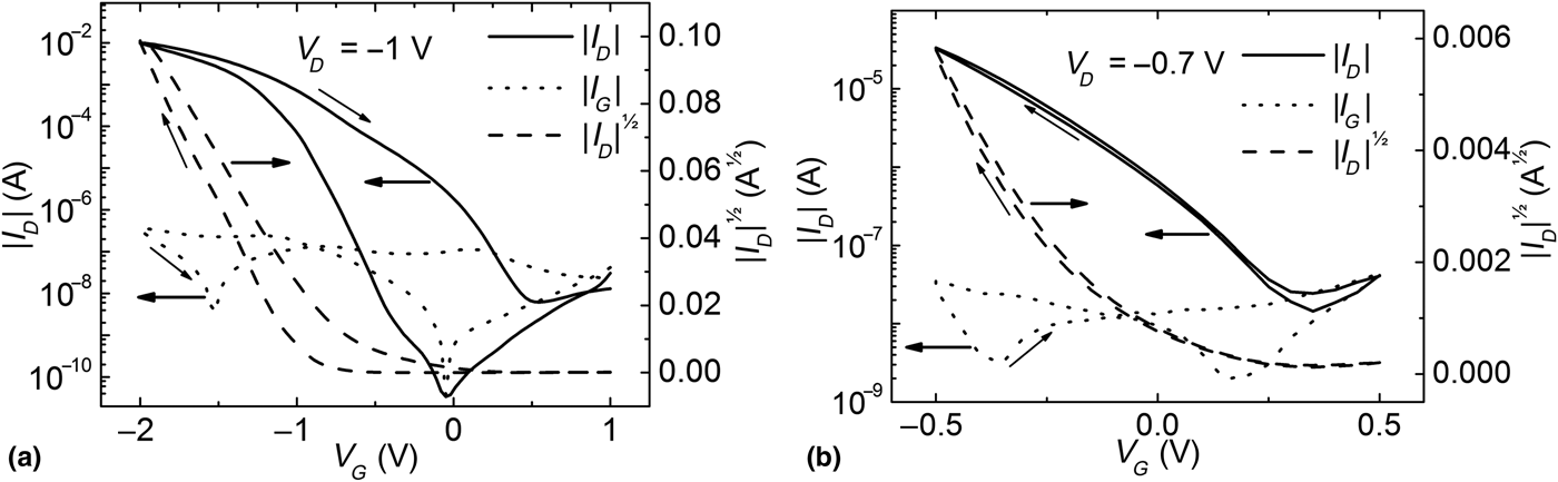
For comparison we present here a transistor made out of pure semiconductor (100:0) and a transistor with low concentration P3HT:PLLA blend (5:95). Typical transfer curves can be seen in Fig. 2. Two general observations can be made of the 100:0 device; it has very high on-currents and show large hysteresis. This is indicative of very slow modulation caused by electrochemical doping.[Reference Larsson, Laiho, Schmickler, Berggren and Crispin19, Reference Lee, Zhang, Lodge and Frisbie20] The transfer curve was measured at 0.5 mV/s. The turn-on voltage for the 100:0 device lies around zero volt and the on/off-ratio is higher than 106. The gate leakage does not exceed 1 µA at any point.
Transfer characteristics of the (a) 100:0 device measured at 500 µV/s and (b) the 5:95 device measured at 100 mV/s in an inert atmosphere. ID and IG stands for the drain and gate currents, respectively.
The 5:95 device was measured at a smaller voltage window than the 100:0 device since it starts to degrade if the gate voltage approaches −1 V, probably due to over oxidation. As a result the on/off ratio (2000) is orders of magnitude smaller than for the 100:0 device. However, the 95:5 device can be measured much faster than the 100:0 device without any significant hysteresis appearing. The gate leakage is also smaller for the 5:95 device.
Two separate mechanisms contribute to the speed of the devices. The first one is the internal resistance of the ion gel. Several dimensional factors will affect ion motion in the gel: the long distance between the channel and gate, the surface area of the gate, and also the thickness and width of the ion gel stripe.[Reference Larsson, Laiho, Schmickler, Berggren and Crispin19, Reference Lee, Zhang, Lodge and Frisbie20] The second mechanism, which is the main reason for the lower speed in the 100:0 device, is attributed to the thickness of the semiconductor on top of/inside the top layer of the paper substrate. In order for the transistor to turn on, anions have to penetrate into the semiconductor and via electrochemical oxidation increase the conductivity. This process of doping the bulk of the semiconductor will be a slow process in a thick semiconductor film. The reverse dedoping process (when the device is turned off) is even slower, as the mobile anions have to diffuse out of the semiconductor. The dedoping process can be made faster if a positive gate bias is applied. In the 5:95 device, the semiconductor is much thinner and any electrochemical oxidation process that takes place will be much faster. The thin semiconductor layer is also the reason for the decrease in the on-current.
If the vertical phase separation, described above, is complete one would expect that there would be large contact resistance between the electrodes and the transistor channel due to the insulator covering the electrodes. As we do not see this contact resistance in the output curves, we argue that there is both vertical and lateral phase separation occurring at the concentration used, as also discussed by Qiu et al.[Reference Qiu, Lim, Wang, Lee, Hwang and Cho11] for P3HT:poly(methyl methacrylate) (PMMA) blends, even though the water contact angle of PLLA is smaller than PMMA (70° and 74°) and should lead to slightly enhanced phase separation compared to P3HT:PMMA. This secures not only an active upper layer (transistor channel) but also vertical conduits through which charges can be injected into the semiconductor from the electrodes. X-ray photoelectron spectroscopy depth profiling and atomic force microscopy (AFM) phase imaging of different concentration P3HT:PLLA blends (supplementary information Figs. S1 and S2) corroborates this conclusion. Both the lateral and vertical phase separations are likely more complex than the model presented here. A schematic structure of the phase separation and device structure is illustrated in Fig. 1(a). It is also possible that the roughness of the paper substrate is the reason for the electrical contact between the semiconductor layer and the source and drain electrodes.
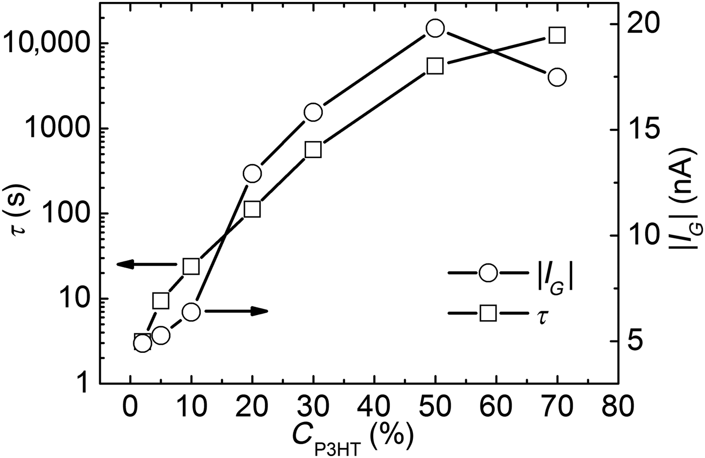
To further elucidate the hypothesis of thinner semiconductor making faster switching devices, we measured the rise times of devices fabricated with different concentrations of P3HT:PLLA blends. In the rise time measurements, the drain current was kept constant at V D = −0.7 V and the gate switched from V G = +0.2 V (off) to −0.5 V (on). The rise time was defined as the time between 10 and 90% of maximum drain current after switching the device on. These rise times and also gate leakage of transistors in on-state taken from transfer curves are plotted in Fig. 3. The rise times decrease rapidly with decreasing P3HT concentration in the blend (Fig. 3), consistent with the fact that the diffusive electrochemical process is getting faster when the anions have shorter diffusion lengths. When the layer is thin the doping process will be fast and saturation will be reached quickly. The same will be true for the reverse dedoping process resulting in low device hysteresis. By comparing the gate leakage in the on-state, taken from transfer curves, also plotted in Fig. 3, it can be seen that the leakage decreases as the semiconductor thickness decreases. This can be a result of the increased insulating layer between the ion-conductor and the source and drain electrodes, and/or decreased displacement current caused by ions moving into the semiconductor.
Open squares represent measured rise times for different concentrations of P3HT:PLLA. The open circles are the measured gate leakages in on-state (V G = −0.5 V, V D = −0.7 V) taken from transfer curves measured at 100 mV/s.
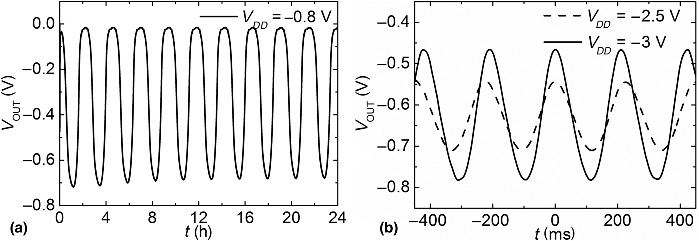
Finally, we show that this effect also is very useful for manufacturing ring oscillators of these transistors directly on the paper substrate. We have used inverters built from 100:0 devices to make a five-stage ring oscillator with the output shown in Fig. 4(a). The operating voltage was −0.8 V and the individual inverters had 205 kΩ drain resistances. To secure that the oscilloscope did not put a load on the inverter a high impedance amplifier (gain = 1) was connected to the output of the ring oscillator. The resulting oscillation frequency was 115 µHz and the propagation delay time, t p = 870 s. This was calculated using P = 2 N t p, where P is the oscillation period and N is the number of inverters. The amplitude of the output signal was measured about −0.35 V and during the 24 h test the signal amplitude only decreased by 5%.
(a) Output of the ring oscillator constructed of five 100:0 devices with 205 kΩ resistors. (b) Output of the ring oscillator consisting of three 5:95 devices with 1, 1, and 2.2 MΩ drain resistors, respectively.
A second three-stage ring oscillator was constructed using 5:95 blend devices. Here we used 1, 1, and 2.2 MΩ resistors as drain resistances in the individual inverters. The operating voltages used were V DD = −2.5 V and V DD = −3 V. The output of the ring oscillator can be seen in Fig. 4(b). At V DD = −2.5 V, the oscillation frequency was 4.4 Hz, the amplitude 100 mV, and the propagation delay time 37 ms. At V DD = −3 V, the corresponding values were 5 Hz, 175 mV, and 35 ms. Although the second oscillator is only three staged and has been measured in air, a general comparison of the speed of the two can, in any case, be made. The propagation delay time was found to decrease from 870 s to 35 ms when utilizing vertical phase separation. Hence, we achieved a four orders of magnitude increase in the device speed in addition to the favorable manufacturing advantages obtained.
Conclusions
We have demonstrated the use of vertical phase separation to speed up ion-modulated organic transistor manufactured on rough and recyclable paper substrates. We have shown that by using a blend of a biodegradable PLLA with the semiconductor P3HT, we solve two main problems with making paper electronics from organic semiconductors, namely that the semiconductor becomes thin and separated from the paper substrate. We can then obtain lower off-currents and faster operation, as demonstrated with the four orders of magnitude increase in operational speed of the OFETs on paper. The ring-oscillators fabricated on recyclable paper using this method oscillate at 5 Hz.
Supplementary materials
For supplementary material for this article, please visit http://dx.doi.org/10.1557/mrc.2014.10
Acknowledgments
We would like to thank Dr. D. Tobjörk for valuable discussions and also acknowledge The Academy of Finland funded Center of Excellence and Functional Materials project (Grant no. 141115), the Tekes funded FlexSens project (Grant no. 40092/09) and Imerys Minerals Ltd., UK, Paramelt B.V., NL, StoraEnso, FI, and Basf, DE for providing the materials used in the multilayer coated paper.