Introduction
Since its discovery in 1912 by Max von Laue, Paul Knipping, and Walter Friedrich,Reference Friedrich, Knipping and Laue1 the now more than a century old technique of x-ray diffraction has become the inescapable tool of choice for probing atomic arrangements in crystalline materials. The formulation of Bragg’s law by William Lawrence Bragg and William Henry Bragg in 1913,Reference Bragg2 which elegantly explains the formation on photographic plates of discrete sets of reflections emanating from the x-ray illuminated crystal, led to the possibility of solving the atomic structure of crystalline compounds and the invention of x-ray crystallography. X-ray diffraction is used today in many forms to characterize materials, including single crystal x-ray diffraction,Reference Woolfson3 x-ray powder diffraction,Reference Dinnebier and Billinge4 and grazing incidence diffraction.Reference Bowen and Tanner5 It is worth noting that all of these techniques use a monochromatized incident x-ray beam, since knowledge of the x-ray wavelength is necessary to obtain the interatomic spacing.
Polychromatic x-ray diffraction, better known as white beam Laue diffraction, although the first to be achieved, turned out to be more difficult to interpret and was, until recently, solely used to orient crystals before their mounting in a diffractometer for monochromatic x-ray study. Laue x-ray diffraction went through a revival in the 1990s along two different directions. First, it was seen as a viable alternative for solving large-unit-cell crystal structures in time-resolved studies. While conventional crystallography requires the collection of hundreds of diffraction patterns as the crystal is rotated to get a usable set of reflections, the same set can be obtained in a single shot with Laue diffraction, as the Bragg condition is simultaneously satisfied for a range of wavelengths.Reference Moffat, Szebenyi and Bilderback6,Reference Helliwell, Habash, Cruikshank, Harding, Greenhough, Campbell, Clifton, Elder, Machin, Papiz and Zurek7 With a method of determining the wavelength of each reflection or “calibrating” the size of the crystal unit cell, Laue diffraction can be successfully used, for instance, to solve the structure of ephemeral macromolecular configurations.Reference Moffat, Helliwell and Mandelkow8,Reference Bourgeois, Vallone, Schotte, Arcovito, Miele, Sciara, Wulff, Anfinrud and Brunori9 Second, it was realized that fast recording of Laue patterns can be used for mapping crystal orientationsReference Wenk, Heidelbach, Chateigner and Zontone10 and strainReference Chung and Ice11 in materials. This technique is called x-ray Laue microdiffraction or micro-Laue diffraction when the x-ray beam size is on the order of 1 μm.
A small beam on the order of or smaller than 1 μm is useful for a range of common materials science problems. These include identifying minute amounts of materials in heterogeneous matrices,Reference Tschauner, Asimow, Kostandova, Ahrens, Ma, Sinogeikin, Liu, Fakra and Tamura12 mapping deformation and phase transformations around a crack tip,Reference Mehta, Gong, Imbeni, Pelton and Ritchie13 or following plastic deformation in small devices such as a metal interconnect line during electromigration (EM).Reference Valek, Bravman, Tamura, MacDowell, Celestre, Padmore, Spolenak, Brown, Batterman and Patel14 X-ray microdiffraction is generally employed to complement other spatially resolving and imaging techniques, as it offers information that is not easily obtainable from other characterization tools. Electron microscopy achieves high spatial resolution, but requires the sample to be in a vacuum and necessitates careful sample preparation.Reference Bozzola and Russell15 None of these restrictions apply to x-ray microdiffraction, as “hard” x-rays (x-rays with wavelength below 4 Å) are highly penetrating (from a few micrometers to hundreds of micrometers in depth depending on the material and x-ray energy range) and samples can, in principle, be measured “as is” without any sample preparation. X-rays can probe buried surfaces such as metal interconnects under a thick layer of dielectricReference Valek, Bravman, Tamura, MacDowell, Celestre, Padmore, Spolenak, Brown, Batterman and Patel14 in a variety of sample environments.
In this article, we first present the instrument settings, including the apparatus and equipment used for Laue x-ray microdiffraction experiments. Next, we describe two fields of applications of the technique for structural characterization. Finally, we present current and expected future developments of the technique.
Synchrotron x-ray Laue microdiffraction
Instrumental setup
An x-ray microdiffraction experiment is preferentially performed on a dedicated instrument at a synchrotron radiation facility (a beamline end station). Small x-ray beams are generated by efficient brightness-preserving x-ray focusing optics, and many different types of such optics have been developed over the years. The most popular are Fresnel zone plates,Reference Myers16–Reference Chao, Kim, Rekawa, Fischer and Anderson19 compound refractive lenses (CRLs),Reference Snigirev, Kohn, Snigireva and Lengeler20–Reference Schroer, Kuhlmann, Hunger, Günzler, Kurapova, Feste, Frehse, Lengeler, Drakopoulos, Somogyi, Simionovici, Snigirev, Snigireva, Schug and Schröder22 and Kirkpatrick–Baez (KB) mirrors.Reference Kirkpatrick and Baez23 However, diffractive optics, such as zone plates, and refractive optics, such as CRLs, typically show chromatic aberration, which makes them unsuitable for focusing polychromatic radiation. The optics of choice for white beam applications are therefore achromatic reflective optics, such as KB mirrors. Below a certain critical grazing angle, x-rays are totally reflected by a smooth, reflective surface. If the surface is bent to a concave elliptical shape, the reflected x-rays converge to a focal point. KB mirrors employ two orthogonal ultrasmooth surfaces coated with a reflective metal layer to focus the beam both horizontally and vertically, and can achieve spot sizes well below 100 nm.Reference Mimura, Matsuyama, Yumoto, Hara, Yamamura, Sano, Shibahara, Endo, Mori and Nishino24,Reference Liu, Ice, Tischler, Khounsary, Liu, Assoufid and Macrander25 A recent development is nested (or Montel) mirrors, where the two mirrors, instead of being separate as in the KB configuration, are combined, resulting in a more compact design.Reference Liu, Ice, Assoufid, Liu, Shi, Khachatryan, Qian, Zschack, Tischler and Choi26
However, even highly efficient optics such as KB mirrors have limited acceptance (maximum incident beam size that can be accepted by the optics) on the order of a few hundred micrometers. This is why micrometer-to submicrometer-sized x-ray beams can only be achieved at synchrotron radiation facilities, where the x-ray beam is both intense and highly collimated. The low divergence of the synchrotron x-ray beam, together with a small angular source size, makes it possible to achieve high demagnification. Since synchrotron x-rays are orders of magnitude brighter than those generated with laboratory sources, photon flux can be “traded” for spot size. Another advantage of synchrotron radiation is its energy tunability, which permits spectroscopic applications. X-ray microdiffraction instruments are often combined with microspectroscopic techniques.
Laue x-ray microdiffraction is best performed with an x-ray synchrotron source, such as a bending magnet (dipole magnet) or a wiggler (periodic structure of dipole magnets) that can provide a continuous spectrum. There are several dedicated x-ray microdiffraction facilities around the world, but only a few have Laue microdiffraction capabilities: the Advanced Photon Source (at Argonne National Laboratory) undulator beamline ID-34 is historically the oldest of this kind still in operation.Reference Ice and Larson27 The superconducting magnet beamline 12.3.2 at the Advanced Light Source facilityReference Kunz, Tamura, Chen, MacDowell, Celestre, Church, Fakra, Domning, Glossinger, Kirschman, Morrison, Plate, Smith, Warwick, Yashchuk, Padmore and Ustundag28 (ALS, at Lawrence Berkeley National Laboratory) was moved in 2008 from an older station on beamline 7.3.3.Reference Tamura, Celestre, MacDowell, Padmore, Spolenak, Valek, Meier Chang, Manceau and Patel29 The European Synchrotron Radiation facility in Grenoble, France has a Laue microdiffraction setup on beamline BM32,Reference Ulrich, Biquard, Bleuet, Geaymond, Gergaud, Micha, Robach and Rieutord30 as does the Pohang Light Source (at Pohang Accelerator Laboratory in Pohang, Korea) on beamline 1B2,Reference Park, Park, Lee, Koo, Shun, Ko, Chung, Hwang and Jeong31 and the Canadian Light Source (at Saskatoon, Canada) on the VESPERS (very sensitive elemental and structural probe employing radiation from a synchrotron) beamline.Reference Feng, Gerson and Ice32 Laue x-ray microdiffraction is also performed occasionally at the Swiss Light Source (at the Paul Scherrer Institute in Switzerland) on the microXAS beamlineReference Maaβ, Grolimund and Petegem33 and the Diamond B16 beamline.Reference Hofmann, Song, Dolbnya, Abbey and Korsunsky34 In the construction, commissioning, or planning stage, are the Taiwan Photon Source (TPS), (at the National Synchrotron Radiation Research Center in Hsinchu, Taiwan) nanodiffraction beamline 21A,35 the Laue microdiffraction projects at the Shanghai Synchrotron Research Facility (in Shanghai, China),36 and the Australian Synchrotron (near Melbourne, Australia).37 We will describe two of these beamlines, the ALS beamline 12.3.2 and the new nanodiffraction beamline at TPS, in more detail.
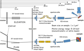
Figure 1 shows an outline of the 12.3.2 x-ray microdiffraction beamline at the Advanced Light Source.Reference Kunz, Tamura, Chen, MacDowell, Celestre, Church, Fakra, Domning, Glossinger, Kirschman, Morrison, Plate, Smith, Warwick, Yashchuk, Padmore and Ustundag28,Reference Tamura, Kunz and Chen38 The x-ray source for this beamline is a superconducting magnet providing a continuous energy spectrum with a critical energy around 12 keV. The first optical element encountered by the x-ray beam is a toroidal mirror, which refocuses the beam at the entrance of the experimental hutch. A pair of slits makes it possible to adjust the source size and thus to vary the x-ray spot size on the sample. A four-bounce monochromator made of two identical silicon (111)channel cuts can be inserted to obtain a monochromatic instead of a polychromatic beam. The four-bounce design ensures that the polychromatic and monochromatic beams follow the same path to the focusing optics and sample, allowing the same spot on the sample to be interrogated by both types of radiation. Final x-ray focusing is provided by a pair of elliptically bent KB mirrors,Reference Sheng, Church, Valeriy, Goldberg, Celestre, McKinneyr, Kirschman, Morrison, Noll, Warwick and Padmore39 giving a routine spot size of 1 μm on the sample in both the horizontal and vertical directions.
Outline of the x-ray microdiffraction beamline (12.3.2) at the Advanced Light Source, Lawrence Berkeley National Laboratory. The synchrotron x-ray beam is focused to submicron size via a pair of Kirkpatrick–Baez (KB) mirrors onto the sample. A four-bounce monochromator can be inserted into the beam path to switch between polychromatic and monochromatic radiation. An area detector and a solid-state detector are used to collect diffraction patterns and x-ray fluorescence, respectively.Reference Kunz, Tamura, Chen, MacDowell, Celestre, Church, Fakra, Domning, Glossinger, Kirschman, Morrison, Plate, Smith, Warwick, Yashchuk, Padmore and Ustundag28

The sample is mounted on high-precision stages to adjust sample position in three directions and at an angle with respect to the beam, allowing high flexibility in the sample positioning and navigation. The x-ray detectors include a Pilatus 1 M detector to collect diffraction patterns and a Vortex silicon-drift detector to collect x-ray fluorescence (XRF) signals.
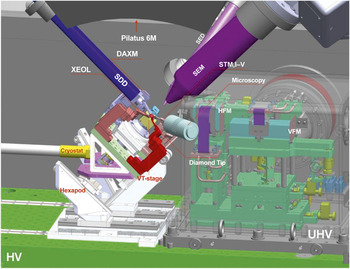
The TPS nanodiffraction beamline 21A follows a similar design, but will offer a wider range of sample-probing capabilities.Reference Liang, Luo, Chen, Huang, Hwang, Wang and Chen40Figure 2 shows a schematic of the future focus x-rays for the microstructure analysis (FORMOSA) end station. FORMOSA provides an all-in-one solution, including differential aperture x-ray microscopy (DAXM), XRF, x-ray excited optical luminescence/Raman/photoluminescence, nanoscale x-ray absorption spectroscopy, scanning probe microscopy, and an indenter to perform in situ and in operando measurements for structural, elemental, optical, electrical, and mechanical properties. The built-in scanning electron microscope and secondary electron detector provide real-time images for sample navigation and positioning. Nominal expected spot size on the sample is 100 nm, provided by fixed-shaped KB mirrors.
An inside view of the future FORMOSA (focus x-rays for microstructure analysis) end station at the Taiwan Photon Source in Taiwan. Note: XEOL, x-ray excited optical luminescence; DAXM, differential aperture x-ray microscopy; SDD, silicon-drift detector; SEM, scanning electron microscope; SED, secondary electron detector; UHV, ultrahigh vacuum; HV, high vacuum; STM, I–V, scanning tunneling microscope, current–voltage; HFM, horizontal focusing mirror; VFM, vertical focusing mirror; VT-stage, ScientaOmicron Inc. VT series stage.

Data collection
Back-reflection Laue is used extensively to determine single-crystal orientation.Reference Greninger41 Spatial resolution provided by x-ray-focusing optics adds new capabilities to this old technique. Samples can be raster scanned under the focused x-ray beam while Laue patterns are taken at each step. Similar to the indexing of arrays of Kikuchi patterns in electron backscatter diffraction, the indexing of the arrays of Laue patterns provides an orientation map of the sample.Reference Wenk, Heidelbach, Chateigner and Zontone10,Reference Chung, Tamura, Ice, Larson, Budai, Brown, Verbruggen and Volkert42,Reference Tamura, Valek, Spolenak, MacDowell, Celestre, Padmore, Brown, Marieb, Bravman, Batterman, Patel, Maex, Joo, Oehrlein, Ogawa and Wetzel43
The use of a large-area detector with one or more megapixels resolution also allows for the possibility of measuring subtle changes in the diffraction peak positions and shapes. From the relative shifts of the Laue spots from their “ideal” positions, as expected from an unstrained crystal, the deformation of the unit cell can be calculated and the full deviatoric (or distortional) strain tensor derived.Reference Chung and Ice11 Scanning x-ray Laue microdiffraction can therefore provide the distribution of the elastic strains in a material. The shape of the Laue spots also contains information about crystal mosaicity as well as plastic deformation. Streaking of reflections along certain directions are generated by geometrically necessary dislocations,Reference Barabash, Ice, Larson and Yang44 while splitting of these same reflections reveals the existence of small-angle grain boundaries. Laue x-ray microdiffraction is therefore ideally suited for spatially resolved studies of mechanical properties of materials.
A further development of scanning Laue x-ray microdiffraction is the addition of depth resolution, which transforms the instrument from a two-dimensional (2D) mapping tool into a three-dimensional (3D) reconstruction tool. DAXMReference Larson, Yang, Ice, Budai and Tischler45,Reference Liu, Ice, Barabash and Ice46 uses a scanning metal wire as a knife-edge to ray-trace back the origin of the diffracted x-ray beams inside the material. A Laue pattern collected at a single location is a composite of all Laue diffractions occurring along the path of the incident x-ray beam, which can penetrate several tens of micrometers into the sample. DAXM deconvolutes the Laue patterns from different depths inside the sample, giving access to the third dimension. The analysis of a DAXM scan produces a volumetric map of crystal orientation and elastic strain in the sample.Reference Budai, Yang, Larson, Tischler, Liu, Weiland and Ice47
Applications of Laue x-ray microdiffraction
With its high sensitivity to crystal orientation, elastic strain, and plastic deformation, Laue x-ray microdiffraction has been widely used to study the microstructure and mechanical properties of small devices such as microelectronic components. It can also be used to completely characterize structural changes during a phase transformation in situ. This section describes some recent applications of the technique in these two areas.
In situ investigation of martensitic transformations by Laue x-ray microdiffraction
Martensitic transformation is a solid–solid phase transformation occurring reversibly between two crystal structures with different symmetries. Materials undergoing a martensitic transformation exhibit shape-memory effects and superelasticity, which are widely exploited for medical devices,Reference Morgan48 microelectronic sensors,Reference Karaca, Karaman, Basaran, Ren, Chumlyakov and Maier49,Reference Srivastava, Chen and James50 and energy-conversion devices.Reference Srivastava, Song, Bhatti and James51–Reference Chen, Cao, Ikeda, Srivastava, Snyder, Schryvers and James54 A major problem with these materials is the lack of phase reversibility upon cyclic loading. Two recent discoveries in ZnAuCu and NiTiCu shape-memory alloysReference Song, Chen, Dabada, Shield and James55,Reference Chluba, Ge, de Miranda, Strobel, Kienle, Quandt and Wuttig56 have revealed a strong microstructure–property correlation (i.e., when the lattice parameters of the material satisfy a set of compatibility conditions);Reference Chen, Srivastava, Dabade and James57 both thermal and mechanical behaviors become completely reversible even after tens of millions of transformation cycles and lead to the formation of rich microstructural morphologies.
Using a thermal stage to quasistatically heat/cool the sample through its phase transition temperature while continuously collecting Laue patterns, the phase transformation pathway from austenite to martensite was tracked for the shape-memory alloy Zn45Au30Cu25Reference Chen, Song, Tamura and James58 by monitoring the spatial variations of specific (hkl) planes as well as the overall change in lattice orientation (Figure 3). The material undergoes a martensitic transformation from cubic (lattice parameter a 0 = 6.1606 Å) to monoclinic (lattice parameters a = 4.458 Å, b = 5.768 Å, c = 40.698 Å, and β = 86.8°) at –40°C.Reference Song, Chen, Dabada, Shield and James55 When the sample is in the pure austenitic phase at −10°C, a strong diffraction peak due to the cubic (206) plane is visible (Figure 3a). Upon cooling through the transition temperature, this diffraction spot splits into three weaker reflections while several other reflections appear. This indicates that the cubic symmetry is breaking down, and the original interplanar distance of (206) is changing. Using the austenite structure to index the Laue pattern in Figure 3b, the center diffraction spot marked by the white box is still found to be the (206) plane. However, other reflections seen during the transitional stage of the phase transformation cannot be indexed either with cubic or monoclinic symmetry. Upon further cooling, these metastable reflections disappear, and new peaks belonging to the monoclinic symmetry of martensite appear, indicating that the phase transformation is complete.
Change in Laue patterns of Zn45Au30Cu25 from (a) pure austenite phase (cubic,  $Fm\bar 3m$) at –10°C, through (b) a transition phase to (c) a pure martensite phase (monoclinic, P21) at –50°C. (d) Stereographic projections of crystallographic planes of the pure austenite phase (red dots), the transition phase (blue dots), and the martensite planes (black boxes).Reference Chen, Song, Tamura and James58

The change in lattice orientation during the phase transformation reveals the average movement of atoms from one crystal structure to the other (i.e., the transformation pathway). Figure 3d shows the stereographic projections of the reciprocal lattices of austenite (red dots), transitional phase (blue dots), and martensite (black boxes) with respect to the rolling (X), transverse (Y), and normal directions (Z) of the sample stage. The sets of red and blue dots in Figure 3d are related by a rotation about the  $(\bar 111)$ axis that maps the reciprocal lattice vectors from austenite to the transitional phase. Due to the structural change, the set of reciprocal lattice vectors of martensite (i.e., the black boxes in Figure 3d) display a combination of stretch and rotation deformation from the cubic-structured austenite. For a martensitic phase transformation, the set of austenite lattice vectors is assumed to be deformed into the primitive lattice vectors of martensite by a macroscopic deformation gradient F such that:
 $$F\,{E_A}L = {E_M}$$,
where EA and EM are the primitive lattice vectors of austenite and martensite, respectively, and L is the lattice correspondence matrix. EA and EM are directly measured by x-ray Laue microdiffraction, while two solutions for L can be computed, from which two possible orientation relationships between austenite and martensite are derived:
 $${\left( {2,0,6} \right)_A}||{\left( {2,0,9} \right)_M}\,or\,{\left( {2,0,11} \right)_M}$$
 $${\left( {0,0,1} \right)_A}||{\left( {1,0,9} \right)_M}\,or\,{(1,0,10)_M}$$
 $${\left( {1,1,9} \right)_A}||{\left( {5,1,36} \right)_M}\,or\,{(5,1,41)_M}$$
 $${\left( {2,1,5} \right)_A}||{\left( {7,2,27} \right)_M}\,or\,{(7,2,34)_M}.$$
Here, (h 1,k 1,l 1)A||(h 2,k 2,l 2)M or (h 3,k 3,l 3)M means that the plane with Miller indices h 1,k 1,l 1 of the austenite is either parallel to the plane of Miller indices h 2,k 2,l 2 or h 3,k 3,l 3 of the martensite.
Application of Laue x-ray microdiffraction in microelectronic materials
In the field of microelectronics, new materials and the corresponding design and processes are constantly being developed for improved chip performance. With its unique capabilities, white beam Laue x-ray microdiffraction has proven to be a powerful tool to investigate a wide range of microelectronics-related materials and structures in situ and in operando.
One of the early applications of Laue x-ray microdiffraction in microelectronics was to study EM of metal interconnect lines.Reference Wang, Cargill, Noyan and Hu59 EM is a diffusion-controlled mass-transport phenomenon driven by momentum transfer between moving electrons and metal ions and is a significant reliability problem for integrated circuits, as the resulting voids can cause the circuit to fail.Reference Ho and Kwok60 In both Al and Cu interconnect lines, Laue x-ray microdiffraction showed that EM-induced plastic deformation in the metal lines manifested as streaking, broadening, and splitting of the Laue reflections.Reference Valek, Bravman, Tamura, MacDowell, Celestre, Padmore, Spolenak, Brown, Batterman and Patel14,Reference Valek, Tamura, Spolenak, Caldwell, MacDowell, Celestre, Padmore, Bravman, Batterman, Nix and Patel61–Reference Budiman, Besser, Hau-Riege, Marathe, Joo, Tamura, Patel and Nix64 It was also found that the occurrence of plastic deformation could be correlated to the availability of 〈112〉 crystal directions in the direction of electron flow along the interconnect lines. When the dislocations generated by plastic deformation are aligned from grain to grain along the interconnect line, they provide an additional diffusion path, further degrading EM performance.Reference Budiman, Besser, Hau-Riege, Marathe, Joo, Tamura, Patel and Nix64
Laue microdiffraction has also been applied to study the response of Sn-based (Pb-free) solders under EM testing. β-Sn has a body-centered tetragonal crystal structure (a = b = 5.84 Å, c = 3.19 Å) and is highly anisotropic. Under EM testing, Sn grains were found to rotate to realign the a-axis with the direction of the electron flow and lower the effective resistance.Reference Chen, Tamura, Tu, Greer, Vlassak, Daniel and Tsui65 However, unlike interconnect lines, little to no plastic deformation was detected in the solder joints. Instead, a buildup of compressive hydrostatic stress was observed at the anode end due to material accumulation transported by the high-density current.Reference Chen, Tamura, Kunz, Tu and Lai66
More recently, Laue microdiffraction has been used to investigate the materials and structures in 3D integrated circuits (3DICs). Three-dimensional integrated circuits utilize vertical integration of two or more dies in order to overcome the basic material and processing challenges in Moore’s Law scaling.Reference Iyer67 In a typical 3DIC, Cu through-silicon vias (TSVs) are used in conjunction with Cu-Sn microbumps to form the vertical connection between stacked dies.Reference Iyer67 For a TSV structure, the mismatch of coefficient of thermal expansion between Cu and Si generates a considerable amount of thermal stress in and around the Cu TSV, causing serious thermomechanical reliability issues.Reference Jiang, Im, Huang and Ho68
In one study, a set of TSVs was annealed at 200°C for 1 h, and Laue microdiffraction was carried out during and after annealing. The thermal stress in Cu, plotted in Figure 4a, shows a strong temperature dependence, which could be related to the microstructure evolution of Cu.Reference Budiman, Shin, Kim, Hwang, Son, Suh, Chung, Byun, Tamura, Kunz and Choo69 Further studies observed local plasticity near the top of the Cu vias after thermal cycling, which could be correlated to the height of via extrusion, and thus provided experimental evidence to verify the underlying plastic deformation mechanism of via extrusion (Figure 4b).Reference Jiang, Wu, Spinella, Im, Tamura, Kunz, Son, Kim, Huang and Ho70 In Si, stress-induced lattice rotation was observed near the wafer surface and surrounding the TSV.Reference Jiang, Wu, Tamura, Kunz, Kim, Son, Suh, Im, Huang and Ho71 This near-surface stress directly affects the mobility of the transistors, requiring defining a “device keep-away zone” around the TSV.Reference Jiang, Im, Huang and Ho68 To quantitatively interpret the stress in Si, a modeling approach was developed that took into consideration the penetration depth of the high-energy x-ray radiation.Reference Liu, Thadesar, Taylor, Kunz, Tamura, Bakir and Sitaraman72 For TSVs of different diameters, the stress was found to decrease with reduced via diameters.Reference Liu, Thadesar, Taylor, Kunz, Tamura, Bakir and Sitaraman73 Laue x-ray microdiffraction also verified that a thick polymeric liner could act as a stress buffer to reduce stress and the driving force of interfacial delamination compared to a conventional SiO2 dielectric liner.Reference Liu, Thadesar, Taylor, Kunz, Tamura, Bakir and Sitaraman73
(a) Deviatoric stress mapping of through-Si vias (TSVs) during (top) and after (bottom) annealing at 200°C for 1 h, and grain orientation mapping after annealing, indicating thermomechanical effects. The numbers below each stress map represent the average deviatoric stress components over the sampled area in MPa.Reference Budiman, Shin, Kim, Hwang, Son, Suh, Chung, Byun, Tamura, Kunz and Choo69 (b) (i) Average peak width (APW) map for a Cu via shows local plasticity near the top of the TSV, with (ii) the broadening of a Cu 024 Laue diffraction shown. (iii) Out-of-plane orientation (∆φ) map for Si surrounding the via indicates lattice bending around the TSV.Reference Jiang, Im, Huang and Ho68 Note:  ${\rm{\sigma }}_{XX}^\prime$,
 ${\rm{\sigma }}_{YY}^\prime$,
 ${\rm{\sigma }}_{ZZ}^\prime$,
 ${{\rm{\sigma }}_{XY}}$,
 ${{\rm{\sigma }}_{XZ}}$, and
 ${{\rm{\sigma }}_{YZ}}$, deviatoric stress components in the sample coordinate system.

Current and future developments
With the development of fast area detectors, it is now possible to scan large portions of a sample in a reasonable amount of time. For example, the MAR133 charge-coupled device detector, in service on the ALS beamline 12.3.2 until 2008, had a readout time of approximately 5 s, so it took about 4 h to collect a 50 × 50 μm2 area of the sample using a 1-μm step size (2500 points) and a 1 s exposure. Today, with the Pilatus 1M hybrid pixel detector, which has virtually no readout time, it takes only 45 min to scan the same area.
As detector technology progresses toward smaller pixels and higher efficiency and x-ray sources become brighter, data-collection time will decrease even further. Scans of large portions of a sample result in a “big data” problem, shifting the bottleneck from data collection to data processing. Laue microdiffraction facilities increasingly rely on the availability of large data storage and high computational speeds. The ALS, for instance, is collaborating with the National Energy Research Scientific Computing Center (at the Lawrence Berkeley National Laboratory) for real-time processing of Laue diffraction data on multicore machines.Reference Deslippe, Essiari, Patton, Samak, Tull, Hexamer, Kumar, Parkinson and Stewart74
The combination of fast data collection and speedy data analysis drives the transition of Laue microdiffraction from a scanning x-ray microdiffraction mapping tool toward a real-time quantitative imaging technique for texture, strain, and defect density. Figure 5 gives an example of data acquired on the ALS beamline 12.3.2, showing the transition in a portion of a single-crystalline nickel-based superalloy repaired by laser-assisted 3D printing, from epitaxial grains growing as columnar dendrites to a “stray” grains polycrystalline region with random crystal orientations.Reference Li, Qian, Xue, Wan, Zhang, Tamura, Song and Chen75,Reference Xue, Zhang, Li, Qian, Wan, Qi, Tamura, Song and Chen76 The 20,000 Laue patterns collected on that sample were analyzed on a 48 nodes Linux cluster in around 2 h.
Laue microdiffraction maps of a laser-assisted 3D printed Ni-based superalloy showing the transition from a columnar dendritic region to a polycrystalline region. From left to right, crystal orientation, high-angle grain boundaries, low-angle grain boundaries, and deviatoric diagonal stress component maps.Reference Li, Qian, Xue, Wan, Zhang, Tamura, Song and Chen75 Note:  ${\rm{\sigma }}_{XX}^\prime$,
 ${\rm{\sigma }}_{YY}^\prime$, and
 ${\rm{\sigma }}_{ZZ}^\prime$, deviatoric stress components in the sample coordinate system.

Two other emerging areas derived from the x-ray Laue microdiffraction technique are structure solution of inorganic compounds with a broad bandpass beam (“pink” beam) and serial crystallography with a few percent energy bandpass at Free Electron Laser (FEL) facilities, both taking advantage of fast data collection, offered by a nonmonochromatic x-ray beam, as described.
Structure solution of inorganic compounds with Laue microdiffraction
As new materials become increasingly sophisticated and complex, their structural characterization becomes more difficult. For example, crystals may not be of sufficient quality for conventional single-crystal data collection. They may be embedded in a heterogeneous matrix or in a constrained environment (e.g., a high-pressure cell). Laue diffraction experiments are an attractive alternative to conventional monochromatic single-crystal structure analysis because they not only take full advantage of the synchrotron x-ray energy spectrum, but also do not require controlled rotation of the crystal in the small x-ray beam. By using a broad-bandpass x-ray source, a large number of reflections can be recorded simultaneously in a single exposure (Figure 6a).
(a) Ewald construction for Laue mode (5–24 keV), monochromatic mode (12 keV), and 4% bandpass mode (average energy E = 12 keV). Accessible reflections fall into the shaded areas. (b) Incident flux curve (red, convoluted with the detector response), determined from a single Laue pattern of calcite. The theoretical calculated incident white beam flux is also displayed for comparison.Reference Dejoie, Kunz, Tamura, Bousige, Chen, Teat, Beavers and Baerlocher77 (c) Distribution of the ratio between the intensity of the (41 $\bar 6$) reflection of the orthorhombic phase to the intensity of the (81$\bar 9$) of the monoclinic phase, I(41
 $\bar 6$)/I(81
 $\bar 9$), over an indigo-doped silicalite single crystal. The increase in the intensity ratio from the orthorhombic to the monoclinic domain is consistent with the space group Pnma.Reference Dejoie, McCusker, Baerlocher, Abela, Patterson, Kunz and Tamura79 Note: E max, maximum energy; E min, minimum energy.

However, determining the structure factors from the reflection measured intensities, as is required for structure analysis, is not straightforward. In order to properly interpret the intensities, various issues such as the deconvolution of harmonics, the correction for energy-dependent factors (such as absorption and a geometrical wavelength-dependent factor called the Lorentz correction), and the precise determination of the effective incident spectrum have to be addressed. For small molecule and inorganic samples, the use of precorrected Lorentz and polarization factors, combined with the “reverse method” based on the use of a single Laue pattern of a well-known crystal, has been devised (Figure 6b).Reference Dejoie, Kunz, Tamura, Bousige, Chen, Teat, Beavers and Baerlocher77
Using the described methodology, the crystal structure of an indigo/silicalite organic/inorganic hybrid, an analog of the ancient Maya Blue pigment used in pre-Columbian Mesoamerica, has been determined by combining Laue microdiffraction with powder diffraction.Reference Dejoie, Martinetto, Tamura, Kunz, Porcher, Bordat, Brown, Dooryhée, Anne and McCusker78 In particular, Laue microdiffraction was used to map the indigo distribution within a single crystal. By following the Laue intensity evolution of relevant reflections, both empty monoclinic domains and indigo-induced orthorhombic domains were identified. The Laue diffraction data further indicated that the most probable space group of the orthorhombic domains was Pnma, rather than P212121 (Figure 6c). Structure solution and refinement using Laue microdiffraction data were also carried out for three model samples (sanidine, potassium titanyl phosphate, and ZSM-5 [Zeolite Socony Mobil-5 zeolite]), using a serial snapshot crystallography approach.Reference Dejoie, McCusker, Baerlocher, Abela, Patterson, Kunz and Tamura79 This shows that Laue microdiffraction can be a good alternative to solve and refine the structure of micron-to-submicron crystals when classic crystallography methods cannot be used.
Laue microdiffraction and free-electron laser
With the development of x-ray free-electron laser (X-FEL) sources that create ultrashort x-ray pulses of unprecedented brilliance (number of x-ray photons per second per unit area per unit solid angle per 0.1% bandwidth), a new option for the structural characterization of microcrystalline inorganic materials is arising.Reference Chapman, Fromme, Barty, Whitem, Kirian, Aquila, Hunter, Schulz, DePonte, Weierstall, Doak, Maia, Martin, Schlichting, Lomb, Coppola, Shoeman, Epp, Hartmann, Rolles, Rudenko, Foucar, Kimmel, Weidenspointner, Holl, Liang, Barthelmess, Caleman, Boutet, Bogan, Krzywinski, Bostedt, Bajt, Gumprecht, Rudek, Erk, Schmidt, Hömke, Reich, Pietschner, Strüder, Hauser, Gorke, Ullrich, Herrmann, Schaller, Schopper, Soltau, Kühnel, Messerschmidt, Bozek, Hau-Riege, Frank, Hampton, Sierra, Starodub, Williams, Hajdu, Timneanu, Seibert, Andreasson, Rocker, Jönsson, Svenda, Stern, Nass, Andritschke, Schröter, Krasniqi, Bott, Schmidt, Wang, Grotjohann, Holton, Barends, Neutze, Marchesini, Fromme, Schorb, Rupp, Adolph, Gorkhover, Andersson, Hirsemann, Potdevin, Graafsma, Nilsson and Spence80 Any crystal placed in an X-FEL beam will be destroyed, but not before one diffraction pattern is collected. To obtain a full data set, therefore, many randomly oriented stationary crystals have to be measured. To date, most activity in the realm of structure analysis using a serial femtosecond crystallography approach with X-FEL radiation has focused on macromolecular systems.Reference Schlichting81
The SwissFEL facility,Reference Patterson, Beaud, Braun, Dejoie, Ingold, Milne, Pattjey, Pedrini, Szlachentko and Abela82 scheduled to be operational in 2017, will have a unique feature: The bandpass of the x-ray beam will be adjustable to give as much as a 4% energy spread, an intermediate mode between monochromatic and white beam (Laue) diffraction (Figure 6a). To evaluate the possibility of exploiting this option for microcrystal diffraction of crystals with relatively small unit cells (≤25,000 Å3), data for typical inorganic structures were simulated.Reference Dejoie, McCusker, Baerlocher, Kunz and Tamura83 It was found that with the 4%-energy-bandpass mode, not only can more reflections be recorded per shot, but the intensities can also be measured more reliably. New indexing algorithmsReference Dejoie, Smeets, Baerlocher, Tamura, Pattison, Abela and McCusker84 also showed that individual patterns of up to 10 crystals, measured simultaneously, could be indexed, and intensities could be extracted reliably for structure analysis. This means that even with a single shot, at least a partial analysis of the crystal structure is possible, and this offers tantalizing possibilities for time-resolved studies.
Conclusion
Synchrotron white beam Laue x-ray microdiffraction used in scanning mode has greatly matured as a technique over the last decade. With the ever-increasing brightness achievable at modern synchrotron facilities, progress in x-ray focusing optics, and fast 2D detector technology, as well as the use of parallel computing for near real-time data reduction, Laue x-ray microdiffraction is transitioning from a microstructure mapping tool into a quantitative microstructural imaging tool. Information such as phase, grain orientation, strain, and defect density distribution can be readily obtained from the analysis of thousands of Laue patterns with processing times that are orders of magnitude faster than in the early days of x-ray microdiffraction. The technique today has a wide range of applications beyond the study of the mechanical properties of thin-film materials used in electronic devices. Recent developments include measurements of stress in geological samples,Reference Chen, Kunz, Tamura and Wenk85 mapping of phases and stresses in ancient artifacts,Reference Dejoie, Tamura, Kunz, Goudeau and Sciau86 and orientation imaging in functional materialsReference Ma, Cui, Ueda, Tang, Chen, Tamura, Wu, Fujioka, Tokura and Shen87 and biominerals.Reference Olson, Metzler, Tamura, Kunz, Killian and Gilbert88 As new micro- and nanodiffraction facilities with white beam capabilities are being constructed around the world, it is likely that the use of scanning Laue x-ray microdiffraction imaging will become more widespread across several disciplines.Reference Barabash and Ice89
Acknowledgment
The Advanced Light Source is supported by the Director, Office of Science, Office of Basic Energy Sciences, of the US Department of Energy under Contract No. DE-AC02–05CH11231.