I. INTRODUCTION
It is not possible to develop a brittleness transition model without depending on the many previous studies which have addressed both the experimental data and theoretical criteria from which one gains insight.Reference Lawn1–Reference Samuels, Roberts and Hirsch8 Lawn’sReference Lawn1 original study of single crystal fracture of materials with the diamond cubic lattice followed on by Lawn and Wilshaw’sReference Lawn and Wilshaw2 seminal treatise in 1975 established much of the experimental and theoretical approach to the fracture of brittle solids. Rice and Thomson,Reference Rice and Thomson3 Lin and Thomson,Reference Lin and Thomson4 and RiceReference Rice5 developed criteria for dislocation nucleation from crack-tips for different types of crystalline materials. Armstrong et al.Reference Armstrong, Ruff and Shin6 demonstrated two length scale transitions in single-crystal silicon using differences in indentation contact diameter. Above 3 μm, there was a process of elastic–plastic deformation with cracking. Below 3 μm, there was only elastic–plastic deformation and at even smaller contact diameters of about 80 nm and below there appeared to be little or no plasticity as the load–displacement curve exhibited Hertzian behavior. This was conducted with a 20-μm-diameter diamond ball and so the hydrostatic component under such contacts could have been substantial. Regarding the kinetics of such a process, besides the experimental data of George and ChampierReference George and Champier7 and Roberts and coworkers,Reference Samuels, Roberts and Hirsch8–Reference Roberts and Hirsch10 there have been a number of experimental/theoretical studiesReference St. John11–Reference Xu, Nabarro and Hirth13 strongly suggesting it is the mobility of dislocations away from the crack tip that controls the brittle-to-ductile transition (BDT). From a more general physical chemistry viewpoint, GilmanReference Gilman14 summarized the mobility of dislocations of semiconductors relating the band gap to the activation energy for dislocation motion.
Except for bulk silicon at temperatures in the 700–1000 K regime,Reference George and Champier7–Reference Xin and Hsia12 there have been few studies of the BDT, e.g., at the few micron and submicron regimes.Reference Gerberich, Michler, Mook, Ghisleni, Östlund, Stauffer and Ballarini15–Reference Huang and Gerberich23 Most of these latter studies address a BDT in terms of length scale, i.e., smaller is tougher.Reference Beaber, Nowak, Ugurlu, Mook, Girshick, Ballarini and Gerberich20–Reference Huang and Gerberich23 There is general agreement that dislocation shielding is important in many of these cases and that the activation energy for dislocation nucleation and motion are necessary features. In this context of relatively dislocation free crystals of small size, the initiation of dislocations at a stress concentration or an oxide film crack will produce a slip band with a back stress from emitted dislocations. This shields existing nanocrack or potential crack sites from achieving sufficiently large local stresses to cause fracture. What is not clear is whether a single approach to fracture resistance can be generated which quantitatively models both the temperature and size scale dependence of the transition. An analytical model is proposed here incorporating standard thermally activated rate processes.
The attractive feature of such approaches is they could be applicable to the BDT of other brittle materials as suggested previously.Reference Gerberich, Mook, Carter and Ballarini21, Reference Mei, Suzuki, Kohlstedt, Dixon and Durham24–Reference Mitchell26 Even though dislocation shielding may only apply to a relatively small class of brittle materials with initially low dislocation densities, the importance to semiconductor, Microelectromechanical systems (MEMS) and Nanoelectromechanical systems (NEMS) would be significant. Here, silicon nanospheres,Reference Gerberich, Michler, Mook, Ghisleni, Östlund, Stauffer and Ballarini15, Reference Gerberich, Mook, Perrey, Carter, Baskes, Mukherjee, Gidwani, Heberlein, McMurry and Girshick18, Reference Mook, Nowak, Perrey, Carter, Mukherjee, Girshick, McMurry and Gerberich19 nanopillars,Reference Gerberich, Michler, Mook, Ghisleni, Östlund, Stauffer and Ballarini15–Reference Östlund, Rzepiejewska-Malyska, Liefer, Hale, Tang, Ballarini, Gerberich and Michler17 and microbeamsReference Nakao, Ando, Shikida and Sato16 are used as a test case. It is generally accepted that semiconductors and ceramics are brittle at room temperature. However, recent studiesReference Östlund, Rzepiejewska-Malyska, Liefer, Hale, Tang, Ballarini, Gerberich and Michler17–Reference Korte and Clegg22 have shown that silicon and spinel (MgAl2O4) have brittleness temperatures at or near 300 K. For example, silicon pillarsReference Östlund, Rzepiejewska-Malyska, Liefer, Hale, Tang, Ballarini, Gerberich and Michler17 and spheresReference Gerberich, Michler, Mook, Ghisleni, Östlund, Stauffer and Ballarini15 on the order of 200 nm in size have a BDT at room temperature and spinelReference Korte and Clegg22 has a BDT at or near 450 K. This large lowering of the brittleness transition temperature by about 600 K requires three features:
(i) avoidance of large critical cracks;
(ii) sufficient nucleation of dislocations;
(iii) rapid dislocation velocities.
In the following, we expand the introduction to address each of these key features. Given these proposed features, a theoretical discussion based on dislocation shielding is given for brittle single crystal materials emphasizing silicon. The tacit assumption is that initial dislocation densities are low. This involves a fracture toughness concept and a kinetic model as others have often discussed for bulk materials, particularly regarding silicon at elevated temperatures.Reference George and Champier7–Reference St. John11 Following that, a proposed model will be applied to experimental evidence which largely represents prior published results.Reference George and Champier7–Reference St. John11, Reference Gerberich, Michler, Mook, Ghisleni, Östlund, Stauffer and Ballarini15–Reference Huang and Gerberich23
A. Avoidance of large critical cracks
Critical to the achievement of plastic deformation in brittle solids is a sufficiently high stress to exceed the Peierls barrier for dislocation nucleation and/or motion. As shown in other studies,Reference Gerberich, Michler, Mook, Ghisleni, Östlund, Stauffer and Ballarini15, Reference Gerberich, Mook, Perrey, Carter, Baskes, Mukherjee, Gidwani, Heberlein, McMurry and Girshick18–Reference Beaber, Nowak, Ugurlu, Mook, Girshick, Ballarini and Gerberich20 these high stresses can be achieved either in nanospheres or nanopillars under compression at room temperature. Recent articles on siliconReference Mook, Nowak, Perrey, Carter, Mukherjee, Girshick, McMurry and Gerberich19, Reference Beaber, Nowak, Ugurlu, Mook, Girshick, Ballarini and Gerberich20 spheres and pillars have shown compressive stresses, σ, ranging from 4 to 40 GPa without fracture and on MgAl2O4 spinelReference Korte and Clegg22 pillars from 5 to 7 GPa without fracture at slightly higher temperature. Such stresses have been achieved at least partially because of the length scale refinement of 50 to 2500 nm. However, at 40 GPa in a 50-nm-diameter sphere, the largest crack one could have and not fail at 1 MPa is only 0.4 nm. The underlying rationale here is that if this were a completely brittle material and one had a surface energy, γ, controlling fracture according to Griffith, then a critical stress intensity would be 0.63 MPa
 using
 with E the modulus of elasticity. This would result for a 160 GPa modulus and a surface energy of 1.24 J/m2 ignoring Poisson’s ratio. A larger value of 1 MPa
 was chosen since the materials to be discussed are usually in compression but with wedge cracks. Using
 gives a first order estimate of 0.4 nm for a 2a internal crack. This demonstrates that even relatively small defects were avoided so as to produce large stresses at the smallest scales.
Similarly, for a 2500-nm-diameter MgAl2O4 not to fail at 5 GPa, again assuming 1 MPa , the largest crack is only 25 nm. These crack sizes are only 1/100 of the diameters involved and could easily exist. This strongly suggests that sufficiently large defects were avoided to allow reasonably high stresses to develop under compression. Here, reasonably high should fulfill the second requirement.
B. Nucleation of dislocations
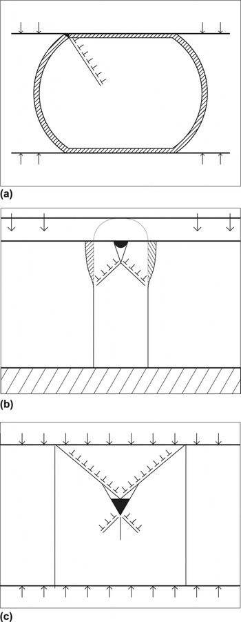
For the preponderant evidence in this study associated with nearly dislocation free single-crystal silicon, dislocations must be nucleated. The requirement then is that sufficient stress must be available to nucleate a dislocation either homogeneously from inside the body or heterogeneously from a surface defect such as a step, a hillock or a contact edge. The above observed stresses are easily in the vicinity of the Peierls stresses reported for both single-crystal silicon (4 GPa), spinel (2.8 GPa), and olivine (5.9 GPa).Reference Mei, Suzuki, Kohlstedt, Dixon and Durham24–Reference Mitchell, Peralta and Hirth27 The assumption is that dislocations are nucleated at any stress concentration site at such high stresses. Possible nucleation sites are surface roughness or contacts which produce increased stresses as in Fig. 1. In Fig. 1(a), the deformation at a contact edge is sufficient to produce nucleation and with multiple dislocations along a given slip band could easily produce shielding at potential crack sites such as a crack in the oxide film. Alternatively, the local plastic deformation initially produced at the apex of a sphere, also shown in the pillar depiction of Fig. 1(b), forms a localized crack and wedges open a central crack which can grow until the crack becomes unstable. This then grows until it arrests. Such a case has been observed in <00l> oriented silicon pillars.Reference Gerberich, Michler, Mook, Ghisleni, Östlund, Stauffer and Ballarini15, Reference Östlund, Rzepiejewska-Malyska, Liefer, Hale, Tang, Ballarini, Gerberich and Michler17 Additionally, Korte and CleggReference Korte and Clegg22 have proposed for appropriate crystallographic orientations that intersecting slip bands can form a Cottrell crack which then nucleates and could arrest as shown in Fig. 1(c). These nucleated dislocations serve several purposes. First, they represent an energy dissipation mechanism and second, from any singular site, provide dislocation shielding to prevent premature fracture. Finally, for special orientations, they could participate in both crack nucleation and arrest. This leads to the third requirement.
Concept of fracture toughness, dislocation shielding and size scale utilizing our rendition of the earlier proposed mechanismReference Korte and Clegg22 with (a) indicating potential shielding at an oxide nucleation site, (b) nucleation at localized-deformation-induced wedge-opening crack, and (c) dislocation mediated internal crack nucleation and arrest.

C. Rapid dislocation motion
Herein lays the key to lowering the brittleness transition to very low temperatures. If a dislocation is emitted from a potential stress concentration site and does not move away from the site rapidly, then a second and third dislocation will have difficulty emitting. This limits the amount of shielding possible. It also restricts the magnitude of plastic energy dissipation. The key aspect is to allow dislocations to move rapidly sufficiently far to allow a number of dislocations to provide shielding. The only way this can happen is if the stresses developed are not only necessary to nucleate dislocations but also sufficiently modify the atomistic process to allow the activation energy (H 0) to be lowered.Reference Zhang and Haasen28–Reference Imai and Sumino41 These would have to be small compared to the nominally large stress free values, H 0, reported for Si (2.2 eV) and spinel (5.5 eV).Reference George and Champier7–Reference Xin and Hsia12, Reference Mei, Suzuki, Kohlstedt, Dixon and Durham24–Reference Alexander, Kolar and Spence33
Considerable attention to the stress-dependent activation energies for dislocation motion abounds in the metals and alloys literature. Except for very high-temperature studies, little evidence is available in the ceramics and geological materials literature. Typical studies, mostly based upon high-temperature studies for silicon and olivine, giveReference Mei, Suzuki, Kohlstedt, Dixon and Durham24, Reference Dodson and Tsao30, Reference Alexander, Kolar and Spence33



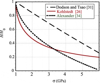
with H 0 the stress free activation energy, τ 0 the shear stress related to one-tenth of the shear modulus or 6.5 GPa, σ p a Peierls stress of 5 GPa, E i of 0.17 eV, and σ 0 equal to 25 MPa. It is emphasized that we have not changed the original authors’ selection of values except for σ0, which was taken as 25 MPa to more realistically represent low temperature data. As shown in Fig. 2, all three models project large drops in the stress-modified activation energy at very high stresses which are known to exist at low temperature. In fact, all three give an activation energy that is too low at the types of stresses plastic deformation is observed in silicon at room temperature. Assuming that some modification is necessary, a relatively standard thermal activation analysis can be proposed as developed below.
Normalized stress-dependent activation energies for dislocation motion H/H 0 as a function of stress for three models of Eq. (1).

II. RESULTS AND DISCUSSION
For the proposed brittleness transition model and application to prior results, we break this into subsections. The proposed model based upon a few dislocation velocity estimates is then followed by application to small-scale fracture toughness results.
A. A proposed brittleness transition model
As suggested above, dislocation emission at potential crack initiation sites is one feature that can lead to high toughness. A fracture toughness model, presented elsewhere,Reference Gerberich, Mook, Carter and Ballarini21 but rederived here in Appendix A is given by

based on a Poisson’s ratio of 1/3. This makes the coefficient in Eq. (2) unity, which only differs by 8% from the derivation in Appendix A if a value of 0.218 were used for silicon. To further relate the fracture behavior to the physical parameters of plastic strain and the activation volume, V *, the number of dislocations are first related to plastic strain and the diameter of the sphere as observed experimentally. This is used to relate K IC to G IC, the strain energy release rate. As shown in Appendix B, this leads to
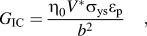
with η 0 ∼ 3. From a mechanics’ perspective, this is satisfying since it suggests that fracture in these nanoscale materials can be nucleated and propagated to failure when the strain energy density, σ ysε p, within the activation volume reaches the strain energy to fracture that same volume. Conceptually, the numerator in Eq. (3) is the local work done and b 2 is the local fracture area to initiate a crack. As a result, local work in the vicinity of crack nucleation concentrated over a region of bonding represented by b 2 represents a work per unit fracture area for crack initiation.
While the above resolves the dislocation nucleation aspect of a brittleness criterion, it states nothing about the kinetics required to address dislocation shielding as dependent upon dislocation velocity. Previously, GumbschReference Gumbsch31 had addressed this for tungsten at low temperatures and Roberts and HirschReference Samuels and Roberts9, Reference Roberts and Hirsch10 extensively for silicon at high temperatures. Neither one of these however, addressed both the length scale and temperature effects in a single model. Here, we propose a standard formulation but require that the activation energy for dislocation motion must either be stress dependent or there is a change in mechanism requiring different activation energies at high and low temperatures. For the latter, there are any number of possible physical explanations such as transitions from the dislocation glide set to the shuffle set as postulated by Kaxiras and coworkersReference Lu, Kioussis, Bulatov and Kaxiras38 and Pizzagalli and coworkersReference Godet, Hirel, Brochard and Pizzagalli34 or for small volumes relying on the single kink nucleation process rather than a double kink for plasticity.Reference Östlund, Rzepiejewska-Malyska, Liefer, Hale, Tang, Ballarini, Gerberich and Michler17 For the purpose of using a stress-dependent activation energy for dislocation velocities in silicon, the model of Alexander et al.Reference Alexander, Kolar and Spence33 was attempted as given by

with slight modifications of the constants so that a large range of temperature could be utilized. Neither this nor any of the stress-dependent functions of Eq. (1) were able to reproduce both high- and low-temperature velocity data. Rather than having a continuously varying stress-dependent activation energy, it was concluded that more likely there was a mechanism change. It was assumed that the high-temperature mechanism had a single activation energy as did the low-temperature mechanism with the latter being smaller. Given this proposed duality of mechanisms, a simplified dislocation velocity law is given by

where H 0 varies with mechanism, being 2.2 eV at high temperature and 0.88 eV at low temperature. Values of v 0, τ 0, and m for both temperature regimes were held constant at 104 m/s, 2 MPa, and 1, respectively. The value of m = 1 at high temperature has been reproduced by a number of investigations.Reference George and Champier7–Reference Roberts and Hirsch10, Reference Xin and Hsia12, Reference Stach and Hull39, Reference Hull, Bean, Peticolas, Weir, Prabakaran and Ogion40 This reproduces both high- and low-temperature data in Fig. 3.Reference Imai and Sumino41, Reference Stauffer42 Reference Reference George and Champier7 for silicon from 520 to 800 °C has m = 1.18 within 10%, Ref. Reference Samuels, Roberts and Hirsch8 has m = 1 to 1.2, Ref. Reference Xin and Hsia12 has m = 1, Ref. Reference Samuels and Roberts9 has m = 1.6 as does Ref. Reference Roberts and Hirsch10, and Ref. Reference Hull, Bean, Peticolas, Weir, Prabakaran and Ogion40 has m = 1. Additionally, Brede and HaasenReference Brede and Haasen43 used m = 1 as well. The authors of Ref. Reference Hull, Bean, Peticolas, Weir, Prabakaran and Ogion40 argued that values of m higher than 1 may result from difficulties in separating the pre-exponential factor m, from the exponential factor. Our position is that 1.0 was acceptable for first-order models. We fully understand that m may be different from unity at low temperatures. As this is unproven, we choose m = 1 to keep the formulation simpler. This is addressed in the limitations section at the end.
Dislocation nucleation as a function of applied shear stress at high and low temperatures.
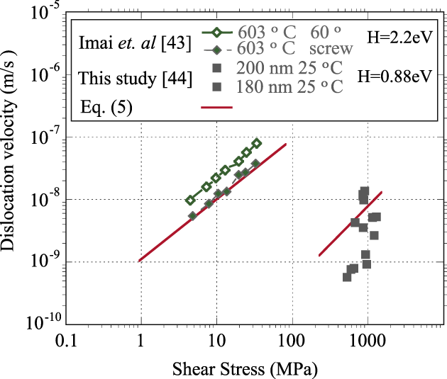
While not a perfect fit for the low temperature regime, the shift in velocities with temperature is reproduced and the general trend with stress is achieved. It is important to consider how the dislocation velocities in silicon at very high stress and very low temperature were measured. The details are in a PhD thesisReference Stauffer42 and have been recently submitted.Reference Stauffer42 Briefly, diffraction bands during in-situ transmission electron microscopy studies of pillars under compression could be measured with respect to their positions before and after loading in the spirit of Johnston and Gilman’s original etch pit studies of LiF.Reference Gilman, Johnston, Fisher, Johnston and Thomson44 Some of these bands could be imaged subsequently in a double-tilt stage to identify that dislocation loops were associated with the diffraction bands. Given the position of the diffraction band prior to and after the deformation cycle as well as the time interval under load, an average velocity could be determined. To check the validity of this approach, one could take the circular loop size of approximately 30 nm and the loading time of 20 s, which requires the velocity to be at least 1 nm/s. Using the above protocol, that is also what was estimated from the data. A caveat is that the dislocations could be moving even faster since the total time under load might be much greater than the actual time the dislocation was moving.
Given that the strain energy release rate from Eq. (3) is related to both yield strength and plastic strain with the latter related to both dislocation velocity and applied stress, it was possible to establish a relationship between fracture and dislocation kinetics. The standard Orowan equation gives

and with a constant strain rate test which was the case for the pillar tests,

Combining Eqs. (5)–(7) gives a standard relationship between the plastic strain and the external variables to be

This allows the dependence of G IC to be related to thermally activated rate parameters by defining a scaling factor of Ψ0 = 3ρv 0∆t/σ 0 given that τ/τ 0 = σ/σ 0 and m = 1. With Eqs. (3) and (8), one finds
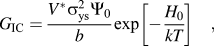
with Ψ0 having units of m/N. This defines a microstructural scaling parameter Ψ0 by using Eqs. (3) and (7) with the proposed relationship that m = 1 to obtain  . By incorporating parameters into Ψ0 and combining this with Eq. (8), one obtains Eq. (9). This is an attractive result as it has the physical parameters of the yielding mechanism, σ ys, V *, b, and ρ as well as the kinetics of dislocation shielding of importance to fracture. It also has the length scale contained within it as fracture energy increases with decreasing length scale. This is due to an increase in yield strength with a decrease in length scale only partially offset by a decrease in activation volume with a corresponding decrease in length scale. For a sphere or pillar diameter, G IC might expect to increase with decreasing diameter.
B. Application to experimental data
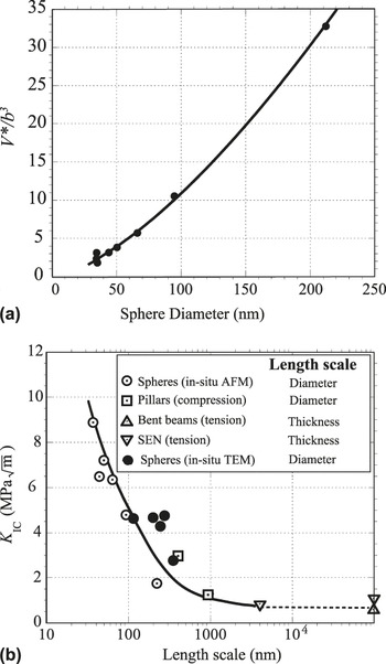
First, consider the length scale transition. In several studies,Reference Gerberich, Michler, Mook, Ghisleni, Östlund, Stauffer and Ballarini15, Reference Östlund, Rzepiejewska-Malyska, Liefer, Hale, Tang, Ballarini, Gerberich and Michler17, Reference Mook, Nowak, Perrey, Carter, Mukherjee, Girshick, McMurry and Gerberich19 it has been shown that fracture toughness, K IC, is inversely proportional to the square root of diameter. Since G IC ∝  , one might expect an inverse diameter relationship for strain energy release rate with size. It had been previously shown that V * is proportional to d and σ ys is inversely proportional to d giving a 1/d dependence. To quantify that, the data previously published by Mook et al.Reference Mook, Nowak, Perrey, Carter, Mukherjee, Girshick, McMurry and Gerberich19 was re-examined using a J-integral approach rather than using a linear elastic fracture mechanics approach. It was determined that the toughness values were about two to three times larger than previously reported.Reference Mook, Nowak, Perrey, Carter, Mukherjee, Girshick, McMurry and Gerberich19 It had also been previously publishedReference Cordill, Moody and Gerberich45 that the activation volume was related to a length scale, d, since the diameter is also related to yield strength as is V *. From previously published data,Reference Cordill, Moody and Gerberich45 a good fit was given by
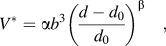
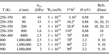
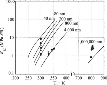
with β = 0.9, α = 5 and d 0 = 25 nm [Fig. 4(a)]. With V * given by Eq. (10) and Ψ0 = 3 × 10¹⁴ m/N, the strain energy release rate was calculated as a function of sphere diameter in Table I. This was then converted to K IC and compared to the experimental values of toughness. These data along with additional nanoscale beams,Reference Samuels and Roberts9, Reference Roberts and Hirsch10, Reference Nakao, Ando, Shikida and Sato16, Reference Hong, Tanaka, Maeno and Higashida46 pillarsReference Xu, Nabarro and Hirth13, Reference Nakao, Ando, Shikida and Sato16 and spheres (Refs. Reference Samuels and Roberts9–Reference Beaber, Nowak, Ugurlu, Mook, Girshick, Ballarini and Gerberich20, Reference Hong, Tanaka, Maeno and Higashida46, this study) are shown in Fig. 4(b). The experimental data from previous sourcesReference Mook, Nowak, Perrey, Carter, Mukherjee, Girshick, McMurry and Gerberich19 was slightly modified from the estimates using a J-integral approach for shallow cracks. Shivakumar and Newman’s elastic–plastic, finite element analysis derived a scaling factor, η pr, which applied to shallow cracks ranging from a/W between 0.05 and 0.5, where W was the width of the sample. See Appendix C. The resulting K IC values are somewhat larger than those reported earlierReference Mook, Nowak, Perrey, Carter, Mukherjee, Girshick, McMurry and Gerberich19 as expected. Whereas gross plasticity was observed prior to fracture, previous estimates were based upon linear elastic fracture mechanics resulting in conservative estimates. The theoretical K IC curve was converted from Eqs. (9) and (10) to find G IC using H 0 = 0.88 eV with T = 300 K. One can consider that a size scale BDT occurred in the vicinity of 100 nm as previously reported.Reference Östlund, Rzepiejewska-Malyska, Liefer, Hale, Tang, Ballarini, Gerberich and Michler17

Parameters used in Eq. (9) for brittleness transition.

a Calculated from Eq. (A9) for nanospheres.
b Estimated from yield strength plot (Ref. Reference Cordill, Moody and Gerberich45).
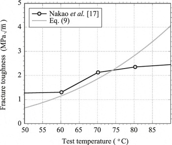
Next consider the temperature effect. Only a few data sets exist for single-crystal silicon where most of the necessary data are available.Reference George and Champier7–Reference St. John11, Reference Nakao, Ando, Shikida and Sato16–Reference Beaber, Nowak, Ugurlu, Mook, Girshick, Ballarini and Gerberich20 For a temperature range of 333–353 K, Nakao et al.Reference Nakao, Ando, Shikida and Sato16 determined the K IC values of 4-μm-thick single crystal silicon beams in bending. As shown in Fig. 5, plane strain fracture toughness increased from 1.3 to 2.4 MPa . This is nearly a factor of four increase in critical strain energy release rate, G IC. Applying the same parameters as were utilized for Fig. 4(b), the fracture toughness as predicted by Eq. (9) is seen to increase over a narrow temperature regime. The significance of using the same activation energy of 0.88 eV to predict the data is that the same dislocation mechanism appears to be appropriate between 300 and 380 K. Considerably different is the high temperature regime in the vicinity of 700 to 900 K. Extensive fracture data from Samuels and RobertsReference Samuels and Roberts9 demonstrated considerable dislocation plasticity at the tips of 15-μm-deep, spark-cut semielliptical cracks. This was in 1000-μm-thick samples and based on elasticity, the K IC was on the order of 2 to 4 MPa
 . Dislocation-produced etch-pitting as produced by up to one hour hold under load clearly indicated the extent of a plastic zone, but it was not clear how far the zone extended at short times. Still, the lower bound elasticity estimate of K IC calculated could be represented by Eq. (9) with an activation energy of 2.2 eV. The high temperature also resulted in lower yield strengths, larger activation volumes, and smaller dislocation densities for these bulk samples with relatively unconstrained volumes. Existing data for a brittleness transition which includes both length scale and temperature was next compared to Eq. (9).
Fracture toughness of 4-μm-thick silicon beams in bending compared to Eq. (9) as a function of test temperature.

A best-effort attempt at choosing values based upon yield strength versus temperature and strain rate is given in Table I. While one can easily criticize the choice of some of the parameters, the largest variation not substantiated by physical measurements are the values of Ψ0 and the activation energy for the low-temperature dislocation mechanism. It is proposed here that the relative constraint in the small versus very large volumes will lead to much larger dislocation densities prior to fracture. This was seen in the nanosphere evaluation where plastic strains of 15 to 40% were experienced prior to fracture. Such deformation could easily increase the dislocation density to 1015 /m2 as was used in the determination of Ψ0 for the low-temperature process. As to the choice of a low activation energy for the low temperature, high stress process, either the switch to the shuffle set plane or a minimal requirement of a single kink rather than double-kink nucleation in small volumes would greatly reduce H 0. Additionally, theoryReference Ewels, Leoni, Hoggie, Jemmer, Hernandez, Jones and Briddon35 has strongly suggested that the rate limiting step for dislocation motion may be reduced by incorporation of hydrogen at the dislocation core, which reduces the energy for kink-pair formation. The overall energy calculated to be 1.16 eV agrees with the measured value of 1.2 eV at low temperature.Reference Yamashita, Jyobe, Kamura and Maeda36 As the low pressure, high-temperature plasma process for making the nanospheres of this study may have resulted in absorbed atomic hydrogen, this might partially explain the low activation energy required as well. Still, the data in Fig. 4(b) contains silicon structures made by several different processing routes including Focused Ion Beam (FIB) fabrication of pillars from bulk silicon. It is not likely that hydrogen would be involved in these.
Irrespective of the detailed mechanism responsible for lower activation energies, Eq. (9) with the parameters of Table I can be compared to the available experimental data.Reference Samuels and Roberts9, Reference Gerberich, Michler, Mook, Ghisleni, Östlund, Stauffer and Ballarini15–Reference Beaber, Nowak, Ugurlu, Mook, Girshick, Ballarini and Gerberich20 In Fig. 6, it is seen that realistic parameters can predict the large shifts in the brittleness temperature transition as observed for various sized nano- to macro-structures. A caveat is that the proposed model was compared to single-crystal silicon formed from a variety of processing routes and tested under various states of stress.

C. Limitations
As with any model attempts using data from a number of sources, there are a number of experimental and states of stress variations that may result in a different set of key variables. Along with different possibilities in how a theoretical model might be constructed, the possible limitations regarding Eq. (9) are:
(i) the activation volume dependence in Eq. (10) could be different using other methods to determine V * than that used previouslyReference Cordill, Moody and Gerberich45;
(ii) with respect to thermal activation, an explicit formulation involving strain rate which depends on the specimen loading rate and therefore incremental time, ∆t, could be used;
(iii) rather than m = 1 in Eq. (8), a stress-dependent exponent different than unity or a stress-dependent activation energy as in Eq. (1) could be used to simulate the behavior at low temperature;
(iv) experimentally, spheres and pillars in compression, bent beams and single-edge notch samples, all with different combinations of Mode I, II, and III stress intensity factors, could easily contribute to the types of scatter and interpretation presented;
(i) a single type of computation study in Appendix A led to Eq. (2) and with the above specimen configuration differences should lead to additional differences in more nearly complete numerical schemes;
(ii) most importantly, activation energies and activation volumes have not been consistently measured on a single batch of silicon, whether intrinsic or doped, at such small scales;
(iii) additionally, electronic doping levels and/or other impurity types could produce variations in the data sets leading to differences in dislocation velocities and therefore the magnitude of dislocation shielding for a given test method.
Given all of these limitations, it is not surprising that only a qualitative match results in Figs. 4–6. Still this gives a guide as to what needs to be accomplished and perhaps much more to understand small-scale effects on the brittleness of semiconductors and other brittle crystalline materials as well.
III. SUMMARY AND CONCLUSIONS
Three factors are shown to allow increased toughness in silicon nanostructures—(i) no initial critical defect, (ii) sufficiently high stress for dislocation nucleation, and (iii) dislocation shielding allowed by high dislocation velocities. As modeled by a thermal activation analysis utilizing activation volume, activation energy, and a one-dimensional, blocked dislocation shielding arrangement, a prediction of the BDT shift by a factor of three in absolute temperature is possible by reducing size. The combination of both length scale and temperature dependence on plasticity can lead to a fracture toughness for silicon at room temperature up to 8 MPa as observed.
ACKNOWLEDGMENTS
The authors acknowledge the Abu Dhabi-Minnesota Institute for Research Excellence a partnership with the Petroleum Institute, NSF/DMR- 0946337, NSF/CTS-0506748, Idaho National Laboratory CON000000029523/#DE/AC07/05ID1517, and the Air Force Office of Scientific Research AOARD-08-4134, for funding. Douglas Stauffer acknowledges Hysitron, Inc.
APPENDIX A
Previous work on dislocation shielding at a crack tip for the emitted slip being blocked at a grain boundary, with grain size, d, is given elsewhere.Reference Gerberich, Mook, Carter and Ballarini21, Reference Huang and Gerberich23 While this was originally conducted for a blocked slip band in a polycrystalline array of grain size, d, here we assume a slip band in a sphere of diameter, d. The basis is the original analysis by LiReference Li47 using the function

where α = 2τ ys/πA; A = μ/ 2π(1-ν); d = blocked slip band length. The physical parameters are τ ys, shear yield strength, μ, elastic shear modulus, and ν, Poisson’s ratio. The spatial parameters coupled to a shielded crack giving rise to mode II fracture toughness, K IIC, are

with b the Burgers vector, c, the nearest dislocation in the band to the crack tip, and S a function of complete elliptical integrals. With Eqs. (A1) and (A2) and relating N shielding dislocations to the mode II fracture toughness, a further conversion to mode I fracture toughnessReference Gerberich, Mook, Carter and Ballarini21 gave

This is the same result reported previously except the fracture toughness was reported as K IC rather than K IIC. Using the appropriate relationship between the two gives the correct relationship at Eq. (A3). Simplifying with a blocked slip band from Eshelby et al.,Reference Eshelby, Frank and Nabarro48 one proposes to first order that
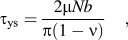
which can be rationalized for the very initial stages of crack nucleation wherein the surface site represents an extremely small crack length. In effect, yielding and crack nucleation are considered as concomitant activities. Interestingly, if one then used Eq. (A4) to eliminate d from Eq. (A3), one finds with ν = 1/3 that the two terms in Eq. (A3) are nearly identical, i.e.,

The assumption here is that τ ys = σ ys/2 since the orientation of a given nanosphere as deposited is random. As the sum of the coefficients is almost exactly unity, we use

which is Eq. (2) in the main text. It is understood that the boundary conditions for nucleating a crack in a sphere are different than those for a crack nucleating at a planar surface of a semi-infinite medium. As such, it would be appropriate to repeat such a derivation using discretized dislocation theory.
APPENDIX B: FRACTURE TOUGHNESS AS RELATED TO PLASTIC STRAIN AND ACTIVATION VOLUME
In particular for the compression of spheres, the Tabor or geometric estimate of contact strains may be used. This can be given by either

with the second formulation biased towards the strains at the top and bottom contacts rather than an average value of δ/ 2R. For strains between 5 and 15 percent, these agree within about 25 percent. For initially dislocation-free spheres, δ ∼ Nb and with Eq. (A6) gives

Using Eq. (A7) to eliminate N in Eq. (2), one finds

With a desire to relate fracture behavior to the physical parameters controlling dislocation nucleation and mobility, an activation volume, V *, is invoked. Previously, V * had been determinedReference Cordill, Moody and Gerberich45 for different size silicon spheres and a resulting empirical fit gives
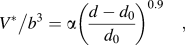
with a cutoff diameter of d 0 = 25 nm, α = 5 and β = 0.9. Such a fit resulted due to the inverse stress dependencies for both d and V *. To simplify and relate V *directly to the nanosphere radius, the data in Table I demonstrate for radii between 40 and 500 nm that

First, the data fit well with η = 1/8. Combining Eqs. (A7), (A8), and (A10) gives
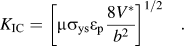
Finally, since the mode I fracture toughness is related to the mode I strain energy release rate, we use standard relationships  and μ = E/2(1+ν) to find

where η 0 lies between 2.7 and 3 for Poisson’s ratio between 1/4 and 1/3. For this study, η 0 = 3 as used in Eq. (3) of the main text.
APPENDIX C
To check the plausibility of using a simpler technique for determining K IC of a sample nanopillar previously published, another three-dimensional (3D) finite element analysis was invoked. The previously published 3D finite element, finite difference technique had obtained a value of 2.9 MPa · Using Shivakumar and Newman’sReference Shivakumar and Newman49 elastic–plastic Finite Element Method (FEM) analysis for shallow cracks, an eta factor is required which is similar to the compliance derivative. With values of η pr for plastic deformation of shallow cracks, the J-integral toughness is given by
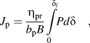
where δ l is the load-line displacement under load, P and bB are ligament and thickness dimensions associated with a rectangular solid. Given the dimensions of the right cylinder, this can be directly used but may be inappropriate given the change in compliance. Nevertheless, the value of bd, where d is the specimen diameter of 400 nm and b is the ligament of 1200 nm, gave a J p equal to 87.5 J/m2 using the 0.6 mN load. Here, η pr ≈ 1 for the 180-nm-long crack. Converting this to K IC gave 3.83 MPa , which is somewhat larger than the linear-elastic fracture mechanics (LEFM) result of 2.9 MPa
 as expected. Based on this similarity, Eq. (Al3) was used for nanospheres assuming that similar wedge-opening cracks resulted as was found for the nanopillars. The surface cracks for the nanospheres were much smaller using surface roughness and oxide film thickness as a guide. This resulted in η pr ≈ 0.3, which gave realistic estimates of the strain energy release rate. A caveat is that one would not expect η pr to be the same for different spheres, which probably accounts for much of the scatter in Fig. 4(b).