Introduction
The worldwide competition to investigate and implement fifth-generation (5 G) cellular systems has escalated, fueled by the potential for groundbreaking improvements in communication technology. These advancements include achieving maximum transmission speeds exceeding 20 Gbps and expanding network capacity by 100 times compared to previous generations [Reference Banafaa, Pepeoğlu, Shayea, Alhammadi, Shamsan, Razaz, Alsagabi and Al-Sowayan1, Reference Cuiñas, Laska-Leśniewicz, Znajdek and Kamińska2]. Such capabilities position 5 G as a transformative enabler for a wide range of industrial applications. However, realizing these ambitious goals introduces significant technical challenges for telecommunication systems. Critical performance indicators including elevated efficiency, extensive bandwidth, significant peak-to-average power ratio, and exceptional linearity are vital to satisfy the rigorous requirements of 5 G applications [Reference Sun, Gao, Zeng, Hu, Liu and Zhang3–Reference Oh, Choi, Shin, Chen, Kang, Woo, Hwang, Lee and Yang6]. Among these, achieving high efficiency has emerged as one of the most critical and challenging aspects, especially in the design and optimization of power amplifiers (PAs) [Reference Fu, Li, Ma, Wu and Lin7].
Power amplifiers are among the most power-intensive components in telecommunication systems, and their efficiency directly impacts overall system performance, energy consumption, and operational costs [Reference Qi and He8–Reference Zahid, Jiang, Lu and Zhang10]. To address these challenges, switched-mode power amplifiers (SMPAs) have been identified as promising candidates for high-efficiency RF amplification. Derived from the Class-D amplifier architecture, SMPAs employ a push-pull configuration where transistors function as switches, alternating between saturation and cutoff states [Reference Zahid, Javed and Feng11, Reference Zhou12]. This approach theoretically enables SMPAs to achieve near-100% drain efficiency [Reference Jianping, Li, Kaiping and Kan13, Reference Park and Lee14]. However, practical implementations are constrained by the non-ideal characteristics of transistors, including parasitic reactances, finite on-resistance, and limited gain, which degrade performance at higher frequencies.
Class-D amplifiers, while highly efficient at audio frequencies, exhibit substantial losses at radio frequencies due to parasitic effects. These losses arise primarily from the energy dissipated during each switching cycle, particularly when transistors have output shunt capacitance. Class-E amplifiers provide a potential solution by leveraging the zero-voltage-switching technique, which eliminates output capacitance discharge losses by ensuring that the voltage across the transistor is zero at the moment of switching [Reference Zahid, Jiang, Lu, Khan and Zhang15]. While effective in the megahertz range, the performance of Class-E amplifiers diminishes at gigahertz frequencies, where the reduced dead time and challenges in timing control pose significant design constraints.
At higher frequencies, the precise control of dead time becomes increasingly challenging due to the shorter available switching intervals. Square-wave gate drive methods, commonly used for timing control, become less effective as switching frequencies approach the megahertz range and beyond. Recent advancements have proposed sinusoidal gate drive techniques to regulate dead time with improved accuracy, offering a promising pathway to extend the operational efficiency of SMPAs into the gigahertz range [Reference Samy, Shawky and Orabi16, Reference Nguyen, Zhang, O’Connell, Staszewski and Walling17]. An unlicensed band of 8.2 MHz is allocated for Electronic Article Surveillance (EAS) system Radio Frequency Identification (RFID) applications. It is an anti-theft technology which is used by merchants against shoplifters. This frequency falls within the 7.4–8.8 MHz band, and this band is internationally designated for Short-Range Devices (SRD) including inductive RFID applications. As outlined in several standards, such as ETSI EN 300 330 [18] and International Telecommunication Union (ITU) ITU-R SM.1538-4 [19].
This study presents a comprehensive theoretical analysis and complete design of a high-efficiency push-pull Class-D MOSFET PA, meticulously tailored for RFID applications. The proposed amplifier operates within a frequency range of 7.7–8.7 MHz, designed to optimize power-added efficiency (PAE) and deliver enhanced output power at the desired levels. The overall structure of this study is precisely arranged to lead the reader through the essential elements of the design and its performance assessment. Section “Losses in Switching PAS” provides an overview of losses in switching amplifiers, offering insight into the challenges addressed in the proposed design. Section “Theoretical analysis and design of CDPA” outlines the theoretical foundation and design considerations for Class-D power amplifiers (CDPAs), while Section “Working principle of the proposed RF PA circuit design” explains the working principle of the proposed RF CDPA circuit. In Section “Experimental results”, the experimental results and simulation outcomes are discussed, validating the design’s effectiveness. Finally, Section “Conclusion” encapsulates the study by summarizing the principal findings and their potential implications for future developments in RF PA technology. This work highlights the potential of push-pull Class-D configurations for achieving high-efficiency RF amplification, demonstrating their suitability for RFID systems and contributing to the ongoing development of energy-efficient RF solutions.
Losses in switching PAS
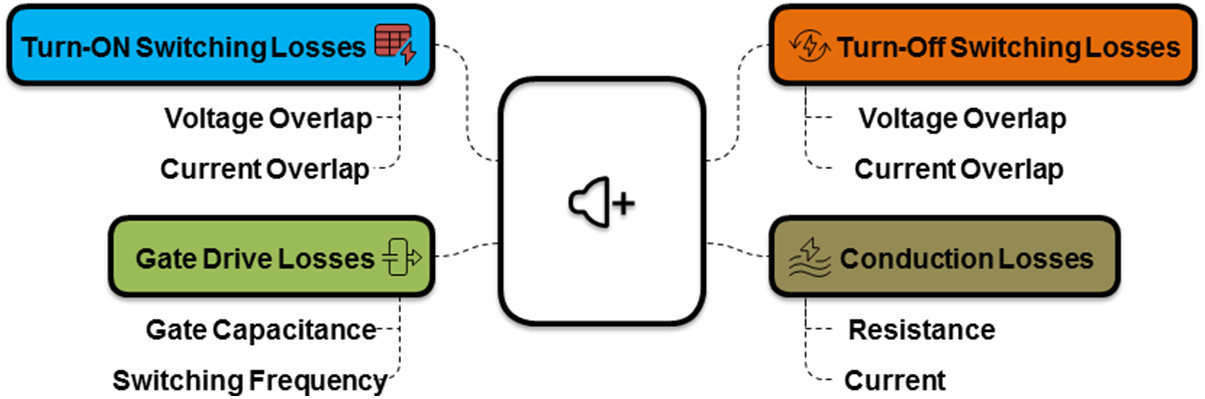
SMPAs, such as Class-D amplifiers, are theoretically capable of achieving 100% efficiency under the assumption that all switching devices operate ideally. Unlike traditional Class A, B, and C amplifiers, which inherently suffer from significant losses due to their linear operating modes, SMPAs eliminate these losses through their switching operation [Reference Lee and Lee20, Reference Lee, Park and Lee21]. However, ideal devices and components do not exist in practice, leading to inevitable power losses. This section examines the key loss mechanisms in switching PAs as show in Fig. 1, with a focus on their behavior at radio frequencies.
Losses in power amplifier.

Turn-ON switching losses
There will be reduction in power when a switch goes from its off-state; there is a significant voltage present at the terminals, yet the current remains absent in the active state, a lower voltage and rising current towards a stable value during the changeover. A crossover period occurs when the voltage and current are nonzero, which occurs if the transition is not immediate. Because energy is lost during each switching cycle, the power losses caused by this overlap are proportional to the crossover period and switching frequency [Reference Lee, Park and Lee21].
In Class-D amplifiers, these crossover losses are generally insignificant because the turn-on transition typically occurs at a zero-current crossing, thereby minimizing the overlap between voltage and current waveforms. However, a critical factor contributing to losses during the turn-on phase is the discharge of energy that is retained in the output capacitance (C o) of the switching device. In MOSFETs, the intrinsic capacitance, created by the drain-to-source and drain-to-gate capacitances, stores energy while in the off-state, subsequently releasing it during the switching process.
Such losses become particularly pronounced at high operating frequencies, emphasizing the need for careful consideration in the design of high-efficiency PAs to mitigate their impact. The energy stored in C o is given by
 \begin{equation}{E_{\text{d}}} = \frac{1}{2}{C_{\text{o}}}V_{{{dc}}}^2.\end{equation}
The power dissipation caused by the energy discharge during each switching cycle can be mathematically represented as
 \begin{equation}{P_{\text{d}}} = \frac{1}{2}{C_{\text{o}}}V_{{{dc}}}^2\,{f_{\text{s}}},\end{equation}
where V DS is the drain-source voltage, and f s is the switching frequency. This loss mechanism is unavoidable but can be minimized by selecting devices with low output capacitance.
Turn-OFF switching losses
Similar to turn-on, turn-off transitions also involve crossover losses due to nonzero voltage and current overlap during the switching period. However, unlike turn-on, turn-off does not involve the discharge of C o. Instead, losses during turn-off are primarily attributed to parasitic inductances in the circuit. These inductances, present in the device leads and wire bonds, store energy proportional to the current flowing at the turn-off instant. The energy stored in the parasitic inductance (L) is expressed as
 \begin{equation}{E_L} = \frac{1}{2}L{I^2}.\end{equation}
The parasitic inductance, represented as L, along with the current I present at the moment of turn-off, plays a significant role in energy dissipation. The resulting power loss, which depends on the switching frequency, can be expressed as
 \begin{equation}{P_L} = \frac{1}{2}L{I^2}\,{f_{\text{s}}}.\end{equation}
Unlike capacitive losses, which are intrinsic to the device, inductive losses can be reduced through optimized circuit layout and low-inductance packaging designs.
Conduction losses
Conduction losses arise due to the resistive components present in semiconductor devices, inductors, and capacitors. These losses are not influenced by switching frequency, as the skin depth at radio frequencies remains significantly larger than the physical dimensions of the devices. Therefore, conduction losses remain relatively constant across different operating frequencies and are influenced primarily by the on-resistance (R DS(on)) of the transistors and the equivalent series resistance of passive components.
Gate drive losses
At lower operating frequencies, MOSFETs require minimal gate drive power, contributing to their high efficiency. With an increase in switching frequency, the power consumption associated with the charging and discharging of the gate capacitance becomes increasingly significant. The energy stored in the gate capacitance (E G) for each switching cycle can be calculated as
 \begin{equation}{E_{\text{G}}} = \frac{1}{2}{V_{{{GS}}}}{Q_{{G}}}.\end{equation}
Here, Q G represents the total gate charge, while V GS indicates the voltage between the gate and source terminals. The overall power loss associated with gate drive can be expressed as
 \begin{equation}{P_G} = \,{V_{GS}}{Q_G}\,{f_s}\end{equation}
This loss occurs during each switching cycle as the gate is charged and discharged, dissipating energy in the gate drive circuit resistances. To minimize gate drive losses, designers often employ optimized gate drive circuits with lower resistance and faster switching times.
Theoretical analysis and design of CDPA
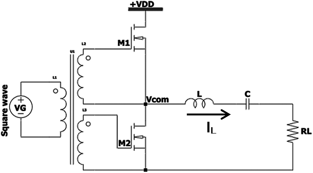
A voltage-switching CDPA operates using a pair of power devices, typically MOSFETs, connected in a cascaded configuration, as shown in Fig. 2. These devices switch alternately between on and off states, creating the essential switching behavior of the amplifier. The upper MOSFET’s drain terminal receives the input DC voltage (V DD), while the lower MOSFET’s source terminal is grounded. This configuration allows for efficient voltage control across the transistors, facilitating the proper switching operation required for signal amplification in the circuit. A three-winding transformer is employed to drive both devices, ensuring appropriate polarity on the output terminals so that a single drive signal controls both devices effectively.
Traditional design of switch mode Class-D power amplifier [Reference Zhou12].

The midpoint between the two MOSFETs, denoted as V com, is interfaced with the load circuit, which is typically modeled as a series RLC network. In the traditional design methodology, it is assumed that the resonant frequency of this RLC network is synchronized with the switching frequency of the MOSFETs. This alignment ensures efficient energy transfer from the amplifier to the load, facilitating optimal performance in terms of signal amplification and minimizing power losses [Reference Jianping, Li, Kaiping and Kan13]. Consequently, the switching action produces a square-wave voltage at V com with an amplitude equal to V DD, assuming ideal device behavior.
Because the load network offers low impedance to the fundamental frequency of V com while presenting high impedance to its harmonic components, the current through the load is mainly determined by the fundamental component of the square-wave voltage. The Fourier expansion of the square wave is expressed as
 \begin{equation}\mathop v\limits_{{{com}}} \left( {\omega t} \right) = \mathop V\limits_{{{DD}}} \left[ {\frac{1}{2} + \frac{2}{\pi }\sin (\omega t) + \frac{2}{{3\pi }}\sin (3\omega t) + \ldots\ldots\ldots} \right].\end{equation}
At resonance, the load impedance reduces to the resistive component (RL), and the current through the load is given by
 \begin{equation}{i_L}(\omega t) = \frac{{2{V_{{{DD}}}}}}{{\pi {R_L}}}\sin (\omega t).\end{equation}
Each MOSFET conducts current for half of the switching cycle, so the peak current flowing through each device corresponds to the value calculated in equation (8). This approach ensures that the current is evenly distributed between the two MOSFETs, maintaining efficient switching and minimizing potential distortion in the signal. The corresponding output power delivered to the load can then be calculated as
 \begin{equation}{P_{\text{o}}} = \frac{2}{{{\pi ^2}}}\frac{{V_{{{DD}}}^2}}{{{R_L}}}.\end{equation}
The efficiency of the amplifier in this configuration, considering ideal conditions with negligible switching losses, is derived as
 \begin{equation}\eta = \frac{{{P_{{{out}}}}}}{{{P_{{{out}}}} + 2{P_{{{dis}}}} + 2{P_{{{cond}}}} + 2{P_{{g}}}}}.\end{equation}
In traditional analyses of Class-D amplifiers, switching losses are often neglected, focusing primarily on conduction losses [Reference Jianping, Li, Kaiping and Kan13]. However, in practical implementations, switching losses resulting from device parasitics, including output capacitances and inductances, can significantly impact the overall efficiency. Figure 2 illustrates these losses, which must be carefully addressed in advanced design approaches to improve performance at high frequencies.
Concept of VMCD PA
As shown in Fig. 3, the voltage-mode Class-D (VMCD) PA, more commonly known as a “Class-D” amplifier, functions according to this principle. Figures 3(a) and 3(b) depict the conceptual circuit diagram and its physical execution, correspondingly. This amplifier topology involves two transistors that are driven with a 180° phase shift, facilitating alternating conduction between them. A series resonant filter is incorporated into the design, with its resonant frequency carefully tuned to align with the center frequency of the input signal. This precise tuning ensures efficient energy transfer, optimizing the power delivery to the load while minimizing losses in the system.
(a) Schematic diagram of VMCD PA configuration 1. (b) Schematic diagram of VMCD PA configuration 2. (c) Drain voltage and current waveforms.

Figure 3(c) illustrates the ideal drain current and voltage (V–I) waveforms. A half-wave rectified sine wave pattern is followed by the current through the transistors in this simplified scenario, whereas the voltage across the transistors produces a perfect square wave. However, real-world implementations of this configuration is challenging due to the inherent parasitic output capacitance (C DS) present in the transistors. This capacitance must be charged and discharged as the transistor toggles between its ON and OFF states, which causes deviations from the ideal square voltage waveform. These non-ideal transitions introduce transient current spikes during the turn-on process, creating an overlap between the voltage and current waveforms. This overlap contributes to extra power losses and introduces distortion in the system. The energy loss per switching cycle (E c) associated with the output capacitance can be expressed as
 \begin{equation}{E_{\text{c}}} = \frac{1}{2}{C_{{{DS}}}}.V_{{{DS - off}}}^2.\end{equation}
V DS refers to the voltage across the drain-source terminals at the instant the transistor switches on, whereas C DS stands for drain-source capacitance.
At higher frequencies, especially in the hundreds of megahertz range, this capacitance-induced loss becomes the dominating contributor, and it is independent of the transistor’s channel resistance. As a result of these restrictions, Class-D amplifiers are not ideal for gigahertz-frequency uses. When the current is zero at the moment of switching, inductance-related losses are eliminated, making zero-current switching (ZCS) another crucial switching condition, and can obtain ZCS with either a VMCD or a Class-F amplifier. In most cases, though, zero-voltage switching (ZVS) is more important for efficient operation since it reduces capacitive losses during transitions by making sure the voltage across the switch is zero [Reference Lee and Lee20].
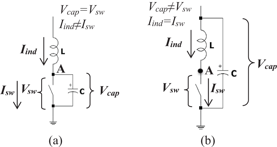
Figures 4(a) and 4(b) illustrate various switch models incorporating parasitic capacitance and inductance across different topologies. Capacitance voltages are identical to switch voltages in Fig. 4(a). If a non-zero voltage exists when the switch turns ON, energy loss occurs. To prevent this, ZVS must be maintained at node A. Conversely, Fig. 4(b) shows a case where the capacitance loss is avoided but inductance-related losses cannot be eliminated without ZCS at node A. In practice, transistor behavior aligns more closely with Fig. 4(a). Moreover, in integrated circuit (IC) implementations, the parasitic drain inductance can be minimized, improving overall efficiency [Reference Pezeshkpour and Ahmadi22].
Switch models.

Working principle of the proposed RF PA circuit design
The proposed RF PA plays a key role in the EAS system, designed to operate efficiently within the frequency range of 7.7 to 8.7 MHz. Figure 5 presents the block diagram of the proposed PA, while the Fig. 6 shows its schematic diagram. Its primary function is to amplify low-power RF signals to sufficiently high power levels, ensuring robust signal strength for transmission through the surveillance antenna. To achieve this, the design employs a multi-stage architecture, where each stage is tailored to specific roles such as signal amplification, impedance matching, and stability enhancement. A detailed analysis of the circuit’s operation is discussed in the following sections.
Proposed RF CDPA.

Schematic diagram of the proposed RF CDPA.

Input and driver stage
The input RF signal is initially processed by a driver circuit build using two complementary transistors (2N3904 and 2N3906). This stage not only amplifies the incoming signal but also provides the proper biasing needed to drive the subsequent high-power stages. Additionally, the driver stage acts as a buffer, isolating the signal source from the power amplification stages, thereby preserving signal integrity.
The bipolar junction transistors (2N3904 and 2N3906) used in this stage contributes to pre-amplification and signal conditioning. Capacitors (C 1 and C 2) are employed as coupling elements, effectively blocking DC bias components while allowing the AC RF signal to pass through. Resistors (R 3 and R 4) define the biasing conditions to optimize the operation of the BJTs. In this configuration, the complementary transistors work together to produce a balanced, higher-amplitude signal. Proper biasing ensures linear amplification, reducing distortion and preserving the fidelity of the RF signal. This stage provides sufficient power to effectively drive the final amplification stage.
Power amplification stage
The main amplification is performed in the power stage using power MOSFETs M 1 and M 2 (both of which are IRF510) capable of handling high voltage and current levels. These MOSFETs are configured to operate in Class D mode, providing an effective balance between efficiency and linearity. Class D operation is particularly advantageous for minimizing power loss while maintaining the integrity of the RF signal, which is critical for the performance of the EAS system within its operating frequency band.
To improve the linearity of the proposed CDPA, which incorporates gate drivers (Q 1–Q 4) and a level shifter stage (Q 5–Q 10), the main important factor is the use of feedback loop around the switching stage. By comparing the output signal with the input (VP 1 and VP 2) and feeding back the error, the nonlinearities of the switching action significantly reduced. The high gain feedback loop ensures the output voltages accurately tracks the input signal and effectively making the CDPA behave like a linear amplifier. Principally, the feedback loop continuously measures the error between the desired output signal and the actual output signal. Then it adjusts the timing of the switching action to correct this error. This continuous correction efficiently cancels out the non-linearities characteristic to the switching process.
Impedance matching network
The impedance matching network in the proposed CDPA design plays an important role in ensuring maximizing power transfer to the load (RL). After the toroid transformer, a 4-pole Chebyshev bandpass filter configuration is utilized, the central frequency is 8.2 MHz with a bandwidth of 1 MHz (7.7–8.7 MHz). The use of a Chebyshev filter with its equiripple response in the passband allows for a sharper roll-off, providing effective selectivity and minimizing signal distortion within the desired frequency range. This matching network not only ensures optimal power transfer between the amplifier and the load by matching complex impedances but also suppresses out-of-band noise and harmonics, thereby improving overall amplifier performance and stability. The inductors (L 4, L 5, L 6, and L 7) and capacitors (C 3, C 4, C 5, and C 6) in the proposed filter are carefully chosen to achieve the required frequency and impedance characteristics, allowing efficient and stable power delivery at the operating frequency. The overall design parameters of this matching network are listed in the Table 1.
Design parameters of the proposed matching network

Feedback and stability
The stability and linearity of the amplifier are maintained through feedback networks, which include resistors and diodes (e.g., D 1, D 2, and D 4). These components work together to prevent oscillations and ensure consistent performance across the operating frequency range. The feedback mechanism also contributes to maintaining the amplifier’s linear response, which is crucial for achieving high-fidelity signal amplification and minimizing distortion.
In our design, the feedback loop is a closed-loop negative feedback system that operates by sensing the output signal and comparing it to the input. Any difference between these two signals creates an error signal and this error is used to instantly fine-tune the duty cycle of the switching signals (D 1 and D 2), which drives the gates of the MOSFETs (M 1 and M 2). In simple words, this process behaves like a self-adjusting Pulse-Width Modulation (PWM) that ensures the output accurately follows the input. The transformer is fabricated using an FT-50-43 ferrite core with a 5:5:15 turns ratio to efficiently operate at the frequency ranging from 7.7 to 8.7 MHz. This core material is suitable for RF applications up to 50 MHz which ensure low core losses and thermal stability. The FT-50 is a small toroid (0.5” outer diameter) and suitable for CDPA output transformers, because an efficient power transfer minimal heating is critical.
Experimental results
The PA presented in this study was developed and simulated using LTspice and electronic design automation (EDA) tools, enabling detailed performance analysis and optimization. The design takes into account the influence of parasitic elements, which can impact the efficiency and reliability of RF PAs. A key feature of the proposed design is the effective elimination of energy loss in the transistors as heat. This is accomplished by maintaining a clear distinction between the drain voltage and drain current waveforms during operation, which leads to optimal performance efficiency. Figures 7(a) and 7(b) provide a detailed representation of the PCB (printed circuit board) design and its 3D visualization, respectively. The physical prototype is depicted in Fig. 7(c).
Layout of proposed RF CDPA (a) PCB layout (b) 3D view (C) Prototype of fabricated PA.

The simulation outcomes illustrated in Fig. 8 reveal the characteristics of the drain voltage and current waveforms. The current waveform, however, deviates slightly from an ideal square wave due to the presence of parasitic drain–source capacitance. This causes the current to turn negative when the transistor is off, a characteristic attributed to the charge stored in the output capacitance, including the device’s intrinsic parasitic elements. Adjusting for these capacitances could yield a more rectangular current waveform, further improving the amplifier’s efficiency. The simulation demonstrates a PAE of 89.26% while delivering an output power of 49.54 dBm, functioning under a drain voltage (V DD) of 24 V. These results highlight the high efficiency of the amplifier and its suitability for RF applications. This design demonstrates a well-rounded approach to achieving optimal performance, making it a significant contribution to the field of RF PAs.
Analysis of V–I waveforms (a) Ideal V–I waveforms (b) Simulated V–I waveforms for both MOSFETs.

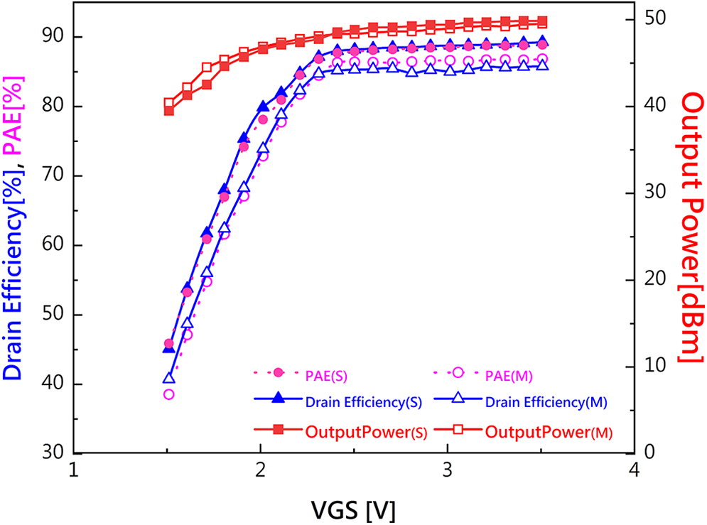
The operational behavior of the proposed CDPA was evaluated by examining the effect of gate-source voltage (V GS) on key performance metrics, including DE, PAE, and output power (P out), as illustrated in Fig. 9. The analysis revealed that the maximum DE of 89.8 % and PAE of 89.26% were achieved at an output power of 49.5 dBm when V GS was 2.5 V. The performance curves indicate a stable and consistent response as V GS approaches 2.5 V, highlighting this value as the optimal operating point. Furthermore, the results show strong alignment between experimental measurements and simulated data, with minor deviations attributed to variations in the parasitic component values. This analysis confirms the reliability of the proposed design and underscores its capability for high-efficiency operation in practical applications such as RF EAS system.
Simulated and measured efficiencies versus gate voltages (V GS).

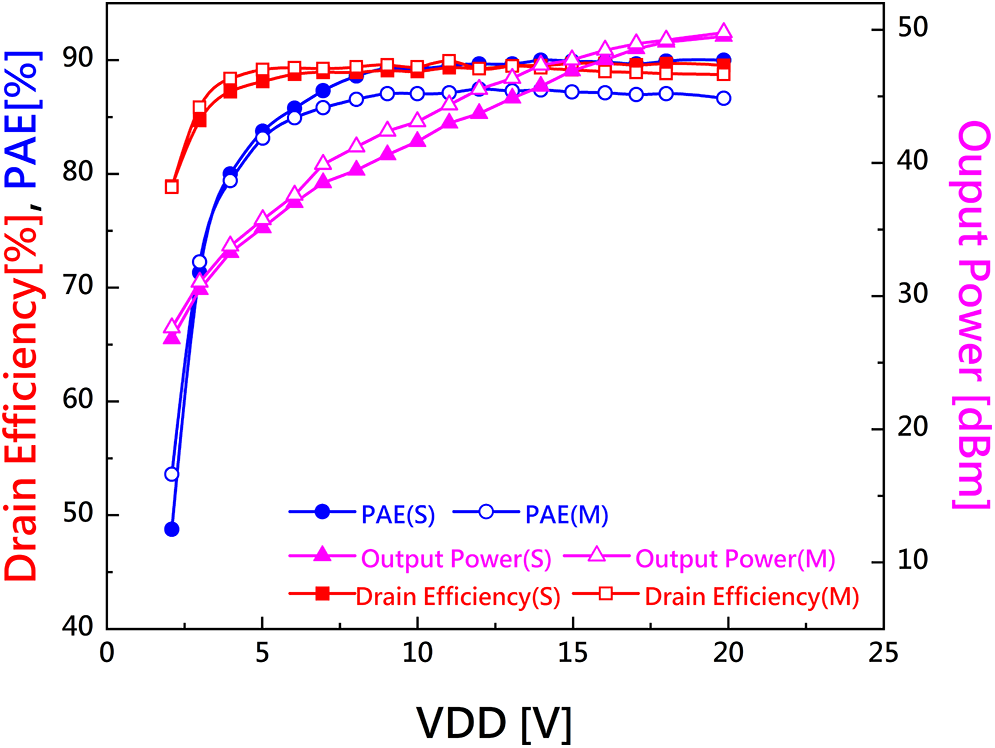
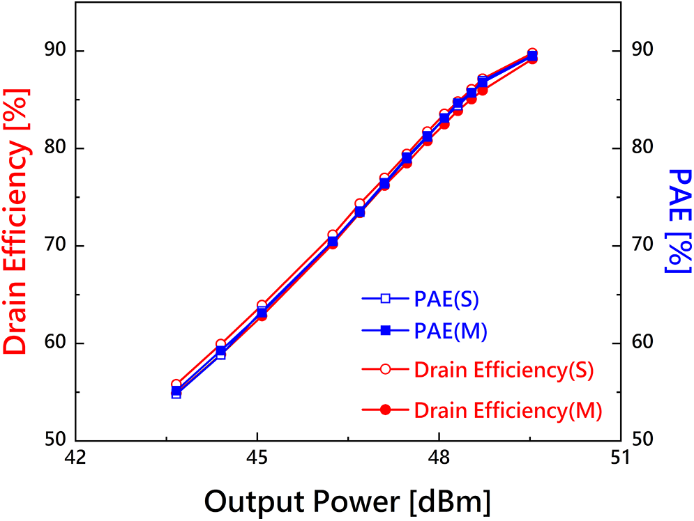
Figure 10 shows the relationship between drain voltages versus DE, PAE and output power at V DD = 24 maximum. At a maximum V DD of 24 V, DE and PAE remain above 89%, demonstrating the high efficiency of the proposed design. Notably, as V DD approaches 10 V, the behavior of DE and PAE stabilizes, exhibiting a flat and consistent response across the range from 10 to 24 V. This stability highlights the effectiveness of the feedback stabilization circuit, which incorporates resistors and diodes (D 1, D 2, and D 4) to suppress oscillations and enhance the amplifier’s reliability. However, at startup conditions where V DD is below 5 V, a noticeable drop in DE and PAE is observed, reflecting the amplifier’s reduced operational efficiency at lower supply voltages. Figure 11 further illustrates the relationship between P out on a decibel scale, DE, and PAE. These quantities exhibit a linear and consistent correlation, reinforcing the robustness of the proposed design in maintaining high performance under varying operating conditions.
Simulated and measured efficiencies versus drain voltages (VDD).

Simulated and measured efficiencies versus output power.

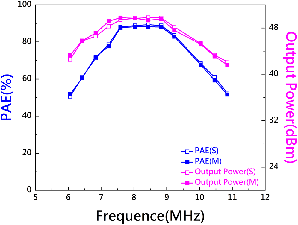
Figure 12 illustrates the frequency dependence of the P out and PAE. The findings reveal a significant correlation between the simulated and measured data, underscoring the robustness and precision of the proposed design. Both metrics exhibit a stable and consistent response across the targeted frequency range, confirming the effectiveness of the amplifier within the desired operational bandwidth. This performance stability is attributed to the efficient impedance matching network, which ensures maximum power transfer to the 50 Ω load while minimizing losses. The robustness of the design underscores its suitability for practical applications requiring consistent high-efficiency operation. A comparative analysis of the CDPA with previously reported designs is presented in Table 2. This analysis underscores the progress made regarding efficiency, output power, and operating frequency, illustrating the advantages of the proposed design in relation to current methodologies.
Simulated and measured power added efficiency and output power versus frequency.

Measured performances in different operating conditions

Conclusion
This study presents an RF PA specifically designed to meet the demanding performance criteria of RF EAS systems. The design incorporates advanced components and optimized subsystems to achieve highly efficient RF amplification with linearity and minimal harmonic distortion. These qualities reflect the precision and innovation inherent in the design, tailored for applications requiring robust RF performance. The amplifier operates effectively over a frequency range of 7.7–8.7 MHz, delivering experimental results that include a maximum DE of 89.8% and P out of 49.54 dBm. These outcomes demonstrate the amplifier’s capability to achieve superior output characteristics across the intended operational bandwidth, establishing its suitability for EAS applications. Additionally, the matching network employed in the design is both straightforward and efficient, ensuring optimal power delivery to the load while simplifying implementation. This well-engineered approach showcases the potential for advancing RF PA technology and provides a significant contribution to the field of RF engineering.
Acknowledgement
This work was supported by the Regional Joint Fund of the Hunan Provincial Natural Science Foundation, China, under Grant No. 2025JJ70309.
Competing interests
The author(s) declare none.

Muhammad Noaman Zahid received his Ph.D. degree with honors from Beijing Institute of Technology (BIT), China, and M.S. degree from Capital University of Science & Technology (CUST), Pakistan, in 2021 and 2015, respectively. He is currently a Technical Expert (TE) with the school of information, Hunan University of Humanities, Science and Technology, located in the southern part of China. His primary area of expertise is RF circuit design and development, and health informatics leveraging RFID technology, and his secondary research interest includes applied electromagnetics, optical communication, and cooperative-intelligent transportation systems. Email: noaman114@bit.edu.cn

Zhu Gaofeng was born in 1979. He received the Ph.D. degree in control science and control engineering from Central South University and is a professor of electronics at school of information of Hunan University of Humanities, Science and Technology. His research interests include in photoelectric detection technology and computer control technology. Email: hnrkzgf@163.com

Wen Yi, male, senior student of Hunan University of Humanities and Science and Technology. During college years, received the National Encouragement Scholarship, the second prize of Electronic Design Competition, and the outstanding student Leader. His research interests include in RF circuit design and development and computer control technology. Email: 3053824450@qq.com

Luo Zhihong is a student majoring in Electronic Information Engineering at Hunan University of Humanities, Science and Technology, with a focus on embedded systems research and practice. He has a solid foundation in hardware development and is proficient in the application of electronic components, PCB design, and hardware debugging. He has actively participated in various project practices and competitions, earning the first prize in the 2024 National Electronics Design Competition. Email: 234091205@huhst.edu.cn

Fayyaz Javed is a postgraduate researcher at Shenzhen Technology University, China. He received his Ph.D. degree from Beijing Institute of technology, China in 2022. His primary area of expertise is optoelectronics and high power solid state laser technologies, working one development of ultrashot mode locked thin disk laser, and secondary research interest is about synthesis and characterization of energy materials. Email: fayyaz022@gmail.com

Li Jiawei is a student of Electronic Information Engineering at Hunan University of Humanities, Science and Technology, with a strong focus on electronic circuit design, PCB layout, and hardware debugging. He has actively engaged in project-based learning and has applied his technical skills in several practical competitions and collaborative projects. Email: 3038952808@qq.com

Syed Raise Akram, an accomplished professional in the field of Electrical Engineering, is driven by a passion for cutting-edge research and innovation. His journey unfolds as a tapestry of academic excellence, hands-on experience, and a commitment to pushing the boundaries of knowledge. Education has been the cornerstone of Syed’s professional journey. He earned his Master’s in Electrical Engineering with a specialization in Electronics System Design from COMSATS Institute of Information Technology (CIIT), Islamabad, Pakistan. Email: raise.akram@comsats.edu.pk