I. INTRODUCTION
With the rapid development of wireless communications, many systems require multifunctional terminals. Such terminals must operate at different frequency bands, and have different polarizations with appropriate radiation patterns. These factors have led to the research into reconfigurable antennas. The properties of the reconfigurable antennas make them adaptable to changing system requirements and provide additional levels of functionality for any system. For example, reconfigurable antennas can improve a weak or noisy connection or redirect the transmitted power to save battery life in portable wireless devices. To configure means to organize elements of something in a particular form or figure. Hence, the reconfigurable antennas are the antennas that can change their operating frequencies, impedance bandwidths, polarizations, and radiation patterns independently according to changing operating requirements. Accordingly, these antennas are classified into three categories: frequency diversity, polarization diversity, and pattern diversity reconfigurable antennas.
Single antenna having the ability of switching between different polarization senses is called polarization diversity reconfigurable antenna. Such antennas received considerable attention over the past decade because of many advantages such as insensitivity to signal orientations and polarization, eliminate signal fading in multipath propagation environments. They are used in multi-system operation in order to reduce number of required antennas, and they can provide double transmission channels for frequency reuse radio transceivers. There are several ways to achieve circular polarization; one way is to excite a geometrically symmetrical antenna by two identical orthogonal modes, another way is to use a single patch antenna which has asymmetry in its structure and excited by two degenerated modes; yet another way is by feeding two identical orthogonal patch antennas in quadrature.
Polarization reconfigurable antennas use switching mechanism to operate in different polarization states. In [Reference Wu, Wu, Lai and Chen1], a reconfigurable aperture-coupled patch antenna with switchable polarization is proposed. They have used the dual-feed structure to provide orthogonal linear polarizations (LPs) and orthogonal circular polarizations (CPs). A single-port reconfigurable antenna capable of modifying the polarization pattern with switch parasitic elements is proposed in [Reference Khaleghi and Kamyab2]. Many other CP reconfigurable antennas are proposed, which have more than one feeding element [Reference Mak and Luk3], several parasitic structures [Reference Donelli, Azaro, Fimognari and Massa4], and several layers below the main radiating patch [Reference Liao, You and Chou5], which makes the design more complex. In [Reference Yoon, Baik, Lee, Pyo, Han and Kim6], a square patch antenna with two L-shaped slots in the ground plane that generates CP is employed and polarization diversity is obtained by altering the current path through switches that selects two L-shaped slots at a time. In [Reference Chang, Lai, Cheng and Hsue7], a polarization diversity antenna that generates six LPs at 30° interval was designed. The main radiating element is a circular patch embedded with a ring slot, which employs 12 diodes that are placed at equal spacing across the slot. In another case [Reference Aboufoul, Alomainy and Parini8], polarization reconfiguration process is achieved by having two feed points which are 90° apart from each other fed to the central circular patch. In [Reference Qin, Guo and Ding9], a modified H-shaped aperture fed to a square patch is employed to get reconfigurable polarization that switches between horizontal, vertical, and 45° LPs in wireless local area network (WLAN) bands 2.4 and 5.8 GHz. A bandwidth enhancement technique for a polarization reconfigurable patch antenna is proposed in [Reference Yang, Yang, Hong and Li10]. In this, a pair of stair case slots with two PIN diodes in the ground plane of a square radiating patch is used to achieve three polarization states namely LP, right-hand circular polarization (RHCP), and left-hand circular polarization (LHCP).
All the above designs are complex and used microstrip feeding technique to achieve polarization diversity. This paper presents a simple, novel, and compact size antenna using geometrically symmetrical patch with less complex design. The main objective of our study is to achieve wide bandwidth using coplanar waveguide (CPW) feeding technique. CPW feed has other advantages beside improved bandwidth such as low radiation loss, less crosstalk between adjacent lines because of presence of ground plane, simplified fabrication, easy surface mounting of active and passive devices (for example, radio frequency (RF) switching devices). This paper is organized as follows. Section II describes antenna geometry and radiation mechanism. Simulated results and discussions are presented in Section III. Finally, Section IV provides conclusions and applications.
II. ANTENNA DESIGN
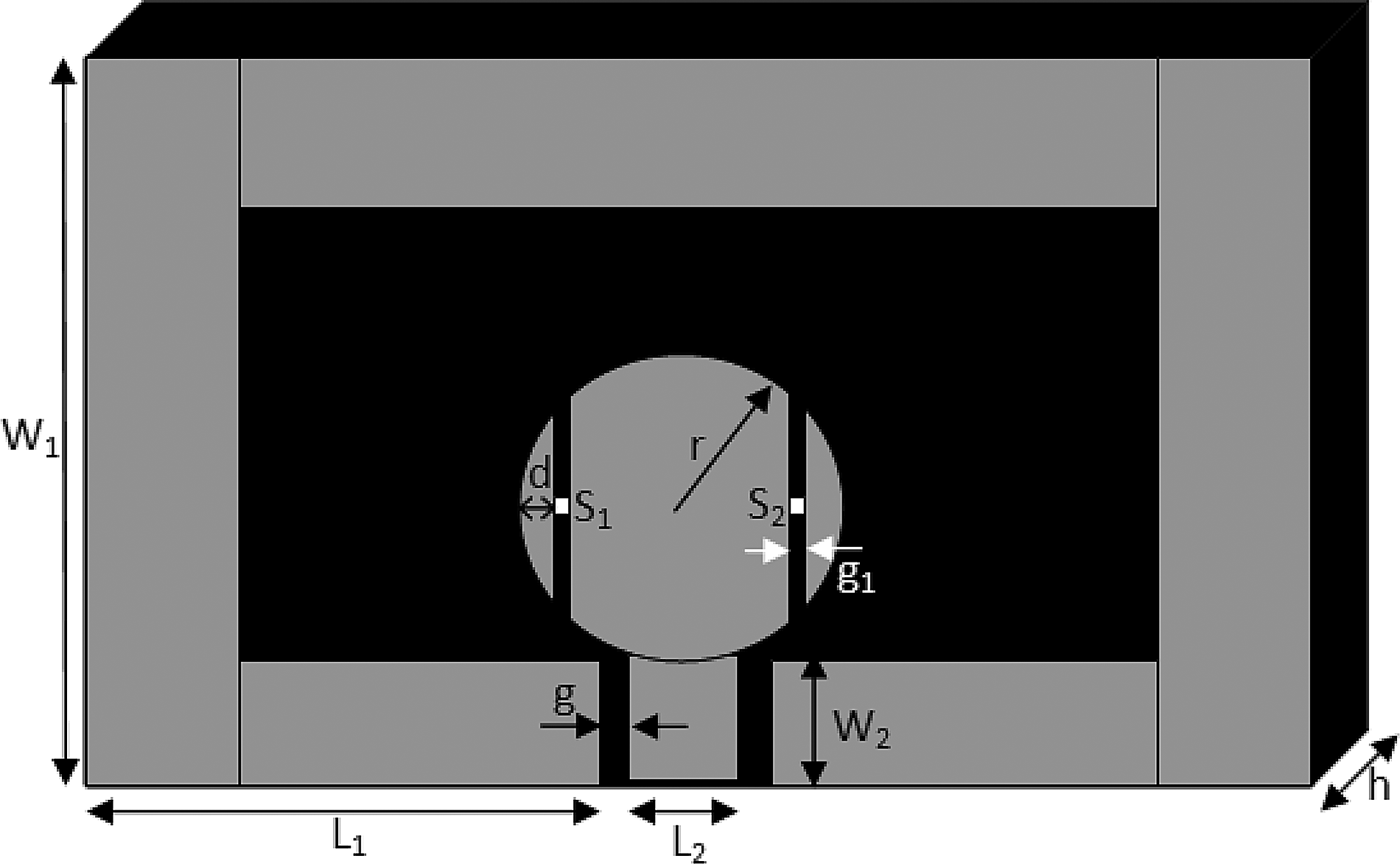
Figure 1 shows the geometry of the proposed polarization diversity reconfigurable antenna. The antenna is designed on a very thin Rogers RT/Duroid 5880 substrate with a thickness of 0.254 mm and having dielectric constant of 2.2. The basic structure consists of a circular patch of radius 6 mm which is fed by CPW feed. The dimensions of the antenna are L 1 = 15.3 mm, L 2 = 3.6 mm, W 1 = 30 mm, W 2 = 7 mm, h = 0.254 mm, g 1 = 0.5 mm, d = 2.0 mm, and CPW ground to feed gap g = 0.4 mm. The size of the antenna is 35 × 30 mm that include radiating patch and the ground.
Structure of the proposed reconfigurable antenna.

At first we have considered an antenna shape (circular-shaped patch) which is geometrically regular and which can be analyzed using simple formulae, and easy to calculate the geometrical properties such as area, etc. The final dimensions of the patch are optimized, to obtain as low return loss as possible for a given frequency/application area. In this case with r = 6 mm, the patch exhibited low return loss at 2.4 GHz (WLAN application). The formula for calculation of resonant frequency ‘f r’ of the circular patch in terms of radius is given by (1).
 $$f_r = \displaystyle{{1.84118c} \over {2\pi a_e \sqrt {\varepsilon _r \mu _r } }}\comma$$
where
 $$a_e = a\left[{1 + \displaystyle{{2\; h} \over {\pi a\varepsilon _r }}\left\{{\ln \left({\displaystyle{{\pi a} \over {2\; h}}} \right)+ 1.7726} \right\}} \right]^{1/2}\comma \;$$
where µr = 1 in this case, ‘c’ is the velocity of the light and a e is the effective radius, ‘a’ is the actual radius of the circular patch and ‘h’ is the thickness of the substrate. The actual radius ‘a’ calculated from the above formula of the circular patch, which resonates at 2.4 GHz is 24 mm but due to introduction of rectangular slots near the two opposite edges, the radius is reduced by four times.
The structure of the basic patch is altered to introduce CP effect. Two degenerated resonant modes which are having 90° phase difference are generated by cutting the original circular patch at 2.0 mm distance from two sides of horizontal diametric edges. These left out patches are connected to the main patch through switches S 1 and S 2. These two switches in the simulation are realized as short copper paths. Presence of the path is treated as ON and absence as OFF. Switch dimensions are chosen to be very small (0.5 × 0.5 mm) so as to realize the practical ON state switch current path. This method provides a good approximation for realization of ON state PIN diode. Table 1 shows the different switch state configurations that allow the antenna to operate in different polarization states.
Different switch configurations for the proposed reconfigurable antenna.

III. SIMULATION RESULTS AND DISCUSSIONS
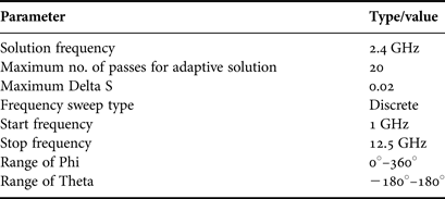
The antenna is designed and simulated using commercial electromagnetic simulator (EM) high frequency structure simulator (HFSS) which is based on the finite-element method numerical technique. In HFSS, to evaluate radiated fields in the far-field region, an infinite sphere that surrounds the radiating object is considered. This is called antenna radiation box inside which antenna resides. The sides of radiation box are placed at λ/4 distance from the main radiating patch. Lumped port excitation is given to the central conductor of the CPW feed of the antenna. The simulation setup details that are considered for analyzing the antenna are given in Table 2.
Simulation setup parameters.
For the case of basic circular patch without switches, the fundamental mode TM11 is excited. The EM simulation observations reveal that by introducing switches in the antenna to accommodate the CP effect, the surface current path gets modified and the fundamental mode TM11 splits into two near degenerate resonant modes.
The antenna in Mode 1, when both switches are OFF, generates vertical LP and resonates at 2.9 GHz. In Mode 2, when S 1 is ON and S 2 is OFF, due to the quasi-symmetrical structure, the slot near the left edge of the circular patch perturbs the current by changing the length of the surface current vector in the x-direction without affecting current vector directed along the y-direction. This makes the fundamental mode TM11 split into two orthogonal degenerate modes with equal amplitude and 90° phase shift and the instantaneous surface current vector on the circular patch rotates and thus the radiated field is circularly polarized. The direction of the current vector is counter clockwise hence the antenna has the RHCP pattern. Similarly, when the antenna operates in Mode 3, i.e. when S 1 is OFF and S 2 is ON, the slot near the right edge of the patch changes the current perturbation and the two degenerated orthogonal modes have equal amplitude and −90° phase shift, which make the surface current vector rotate in the clockwise direction producing the LHCP pattern. Figure 2 shows the surface current distributions on the circular patch in Mode 3, at the switch S 2 at time instances t = 0, T/4, T/2, and 3 T/4.
Surface current distributions of the antenna operating in Mode 3.
A) Return Loss
The return loss curve of the proposed reconfigurable antenna for all the four cases is shown in Fig. 3. It shows that the antenna when operated in Mode 1, resonates at 2.7 GHz. Since both the switches are OFF, its electrical length is small compared to other three cases and hence it resonates at higher frequency. In Mode 4, the electrical length of the antenna is large compared to other cases, hence it resonates at lower frequency 2.38 GHz. When the antenna operates in Modes 2 and 3, i.e. when one of the switches is ON, asymmetry is created in structure and this creates little perturbation of the fundamental mode TM11 and hence the resonant frequency is slightly increased to 2.45 GHz.
Return loss curve for all possible switch configurations.
B) Radiation Pattern
Figures 4(a)–4(d) show the radiation pattern in the elevation plane, i.e. at the x–z and y–z plane cuts for the proposed reconfigurable antenna operating in all the four modes. The patterns are drawn at their respective operating frequencies.
Radiation patterns in the elevation plane.
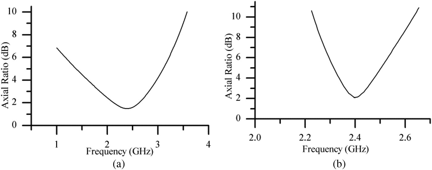
The axial ratio curves of the proposed reconfigurable antenna when it is operated in polarization diversity mode, i.e. in Modes 2 and 3 are shown in Fig. 5.
(a) Axial ratio for Mode 2, (b) axial ratio for Mode 3.
C) Parametric Study
To obtain good results, different parameters of the antenna structure are varied and optimized values are considered. The thickness of the substrate is varied to improve the return loss characteristics, and for impedance matching the feed width is varied. The comparative study of the return loss characteristics for different values of feed width and thickness of the substrate are given in Tables 3 and 4, respectively and their corresponding graphs are shown in Figs 6 and 7. It is observed that the return loss curves were shifted left as the feed width L 2 is increased from 0.8 to 3.6 mm and return loss increased drastically to 40 dB for L 2 = 3.6 mm and when thickness is varied from 0.254 to 1.575 mm there is no appreciable change in resonant frequency, but there is a large increase in return loss for the minimum available thickness. Hence, L 2 = 3.6 mm and h = 0.254 mm have been considered as optimum values.
Return loss curve for different.
Return loss curve for different values of ‘g’ available thicknesses.
Comparison of return loss for different values of CPW ground to feed gap ‘g’.

Comparison of return loss for different values of available substrate thicknesses.

The distance ‘d’ is also varied to study the performance characteristics of antenna. The variation in the return loss and the −10 dB bandwidth, when the proposed reconfigurable antenna is operated in Mode 1, are shown in Fig. 8. For d ≥ 2.0 mm, bandwidth, which is comparable to other cases is obtained and for all other values (i.e. for d < 2.0 mm), a broadband characteristic is obtained.
Return loss curve for different values of ‘d’ when the antenna is operated in Mode 4.
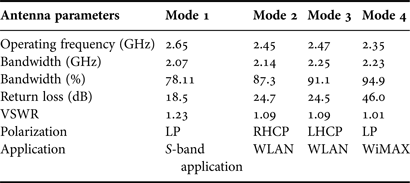
The effective −10 dB return loss impedance bandwidth of 80% is obtained. The simulated results of the proposed antenna are tabulated in Table 5.
Results.
IV. CONCLUSION
This paper presents a simple and compact circular-shaped reconfigurable patch antenna with CPW feed. The antenna switches between LP, RHCP and LHCP. The use of CPW feed to improve the overall impedance bandwidth has been demonstrated using single layer and single feeding element to achieve circular polarization. The proposed antenna has very good return loss, voltage standing wave ratio (VSWR), and impedance bandwidth at the operating frequency band. The antenna operating in Modes 2 and 3 operates at the same frequency and it can be useful in wideband WLAN applications in order to increase number of channels in a given bandwidth and when it is operating in Mode 4, can be used for WiMAX application.
 Ch. Sulakshana was born in Hyderabad, India in 1985. She received her B.Tech. degree (2007) in Electronics and Communication Engineering from the G. Narayanamma Institute of Technology and Science affiliated to Jawaharlal Nehru Technological University, Hyderabad, India. She received her M.Tech. degree (2010) in Communication Systems from the National Institute of Technology, Tiruchirappalli, India and currently pursuing Ph.D. degree from the National Institute of Technology, Warangal, India. Her field of study is Reconfigurable Antennas and other areas of interest are Microwave Engineering and Antenna wave propagation. She has publications in three International Journals, eight International Conferences, and one National Conference.
 L. Anjaneyulu was born in 1967 in India. He obtained his B.Tech. degree (ECE) in 1989, M.Tech. in 1991, and Ph.D. in 2010 from the National Institute of Technology, Warangal, India. He worked as a Project Officer at the Institute of Armament Technology, Pune, India for 5 years from 1991 and involved in the design of Surface borne and Air-borne Radar systems for clutter measurement application. Later, he worked as a Staff Scientist at Helios Systems, Madras, India for 2 years and engaged in the development of Radio Wave propagation assessment software modules for ship-borne radars. He has been with the Department of Electronics and Communications Engineering at the National Institute of Technology, Warangal, India since 1997. His areas of interest include Computer Networks, Electromagnetic Field Theory, Microwave & Radar Engineering, and Neural Networks & Fuzzy Logic Systems. He has completed few defence R&D Projects and has 22 papers to his credit in National and International Conferences and Journals. He is a Life member of ISTE and a member of IEEE, IEEE Antennas, and Propagation Society.