I. INTRODUCTION
Improving the structural and optical quality of AlGaN-based heterostructures with a high Al content (x > 0.5) is a crucial issue for fabricating high-efficiency UV semiconductor emitters operating in the sub-300 nm wave length range. Reference Hirayama, Maeda, Fujikawa, Toyoda and Kamata1 Several approaches have been used by us in a plasma-assisted molecular beam epitaxy (PA MBE) to reduce the threading dislocation (TD) density in the top (active) region of the AlGaN heterostructures grown on c-Al2O3 substrates, to achieve atomically flat droplet-free surface of the heterostructures and enhance the internal quantum efficiency (IQE) of AlGaN quantum wells (QWs). Among them, the application of the high-temperature (HT) (780–790 °C) migration-enhanced epitaxy (MEE) for nucleating the AlN layer on c-sapphire, Reference Nechaev, Aseev, Jmerik, Brunkov, Kuznetsova, Sitnikova, Ratnikov and Ivanov2 the HT metal-flux modulated epitaxy (MME) of thick AlN buffer layers, Reference Jmerik, Mizerov, Nechaev, Aseev, Sitnikova, Troshkov, Kop’ev and Ivanov3 the substrate temperature-modulated epitaxy (TME) during growth of the AlGaN waveguide or barrier layers under the metal(Ga)-rich growth conditions, Reference Nechaev, Brunkov, Troshkov, Jmerik and Ivanov4 and finally the submonolayer digital alloying (SDA) epitaxy for fabrication of the AlGaN QWs of exact composition and with abrupt interfaces. Reference Jmerik, Shubina, Mizerov, Belyaev, Sakharov, Zamoryanskaya, Sitnikova, Davydov, Kop’ev, Lutsenko, Danilchyk, Rzheutskii, Yablonskii and Ivanov5,Reference Jmerik, Lutsenko and Ivanov6 It has resulted in lowering the optical threshold power density from several MW/cm2 down to 150 kW/cm2 for the optically pumped AlGaN mid-UV laser heterostructures grown on c-Al2O3. Reference Ivanov, Nechaev, Sitnikova, Ratnikov, Yagovkina, Rzheutskii, Lutsenko and Jmerik7 Recently, the threshold has been lowered down to the 61–95 kW/cm2 range at λ ∼ 250 nm for analogous AlGaN/c-Al2O3 heterostructures grown by metalorganic chemical vapor deposition (MOCVD). Reference Li, Detchprohm, Kao, Satter, Shen, Yoder, Dupuis, Wang, Wei, Xie, Fischer, Ponce, Wernicke, Reich, Martens and Kneissl8
The paper reports on careful studies of the different stages of PA MBE growth of AlGaN/AlN/c-Al2O3 heterostructures and their structural properties using high-angle annular dark-field scanning transmission electron microscopy (HAADF STEM) and x-ray diffraction (XRD) analysis. The processes of generation of TDs and microdefects at the AlN/c–Al2O3 interface during the initial stage of growth of the AlN nucleation layers (NLs) using the HT MEE are considered in detail. Then, TDs filtering during the two-dimensional MME growth of AlN buffer layers including the ultrathin GaN interlayers is discussed. Different types of compositional inhomogeneities in Al x Ga1−x N waveguide layers of the AlGaN QW laser structures, in particular the ultrathin Al-enriched barrier layers induced by the TME and the spontaneously formed aperiodic compositional modulations along the c-axis for x in the 0.6–0.7 range, as well as the fine structure of the AlGaN QWs grown by the SDA technique were detected by HAADF STEM. They are analyzed from the view point of PA MBE growth and their effect on the photoluminescence (PL) and stimulated emission characteristics of the QW laser structures of different designs, studied by integrated PL and time-resolved PL (TR PL) spectroscopy.
A. Experimental details
The AlGaN single QW (SQW) or double QW (DQW) heterostructures were grown by PA MBE on c-sapphire substrates as described in Refs. Reference Jmerik, Lutsenko and Ivanov6 and Reference Ivanov, Nechaev, Sitnikova, Ratnikov, Yagovkina, Rzheutskii, Lutsenko and Jmerik7. The AlN NLs were grown at relatively high substrate temperatures (T S = 780 °C) using the MEE approach, which is supplied from 3 to 15 monolayers (MLs) of Al per MEE cycle. The AlN buffer layers nucleated on c-Al2O3 using the low-temperature (LT) and HT conventional MBE modes were grown also as the reference samples. The growth of the following 2-µm-thick AlN buffer layer at the same temperature (T S = 780 °C) and under metal-rich conditions proceeded by using the MME technique. Several 3-nm-thick GaN interlayers grown under different stoichiometric conditions were inserted in the AlN buffer layer to verify their effect on reduction of the TD density. The top Al x Ga1−x N waveguide/barrier layers (x = 0.6–0.7) having the thickness around 90–150 nm have been grown under the metal-rich conditions using either the standard (continuous) or pulsed regimes of supplying the growth fluxes. In the latter case, the substrate temperature was temporary increased from ∼690 to 740 °C during periodic growth interruptions for evaporation of the excessive Ga from the surface. But contrary to the droplets-elimination-by-thermal-annealing (DETA) technique proposed in Ref. Reference Terashima and Hirayama9, we achieved simultaneously the substrate heating and the interruption of all the fluxes by closing the main shutter and called this approach as TME. The 2.5-nm-thick Al x Ga1−x N/Al y Ga1−y N SQWs with the nominal QW compositions ranged within y = 0.45–0.53 and the DQW structures with 3 and 5 nm QWs located at the depths of 70 and 120 nm from the surface of the Al0.65Ga0.35N waveguide layer, respectively, were formed by using the SDA technique, which implies the growth of a short-period Al y Ga1−y N/GaN superlattice comprising the ultrathin GaN insertions in the barrier alloy instead of the bulk Al x Ga1−x N QW with the different Al-cell temperatures. Reference Jmerik, Shubina, Mizerov, Belyaev, Sakharov, Zamoryanskaya, Sitnikova, Davydov, Kop’ev, Lutsenko, Danilchyk, Rzheutskii, Yablonskii and Ivanov5 The ratio of the GaN insertion-to-barrier thicknesses d GaN/d AlGaN in SDA growth was kept 1/3 for all the QW heterostructures, which corresponded to an average AlN mole fraction in the QW layer smaller by 15–17% with respect to the barrier. Within the series of three DQW heterostructures, GaN insertion thickness d GaN was varied as 0.25, 0.5, and 1 ML, which corresponded to the SDA periods 12, 6, 3 and 20, 10, 5 in the QWs of 3 and 5 nm, respectively. The QWs in the SQW structures included just three SDA periods with the nominal thickness of GaN insertions of ∼0.83 ML.
All the growth runs were monitored by the reflection high energy diffraction (RHEED) and laser reflectometry. The high resolution transmission electron microscopy (HR TEM) and high-angle annular dark-field (HAADF) imaging were performed with a FEI Titan 80-300 keV electron microscope operated in both HR TEM and scanning transmission electron microscopy (STEM) modes. The measurements of the full width at half maximum (FWHM) of the ω-scans of symmetric AlN(0002) (ω0002) and skew symmetric AlN
 $(10\bar 15)$
 $\left( {{\omega _{10\overline 1 5}}} \right)$
reflections were used to estimate the concentrations of TDs with screw (N
S) and edge (N
E) components, respectively. In accordance with the formula for the random dislocation distributions proposed by Dunn and Koch,
Reference Dunn and Koch10
the TD densities can be estimated as
 $N_{\rm{S}} = {{\omega _{0002}^2 } \mathord{\left {\vphantom {{\omega _{0002}^2 } {4.35\left| {b_{\rm{S}} } \right|^2 }}} \right. \kern-\nulldelimiterspace}/ {4.35\left| {b_{\rm{S}} } \right|^2 }}$
and
 $N_{\rm{E}} = {{\omega _{10\overline 1 5}^2 } \mathord{\left {\vphantom {{\omega _{10\overline 1 5}^2 } {4.35\left| {b_{\rm{E}} } \right|^2 }}} \right. \kern-\nulldelimiterspace} /{4.35\left| {b_{\rm{E}} } \right|^2 }}$
, where
 $\left| {b_{\rm{S}} } \right|$
= c = 0.4982 nm and
 $\left| {b_{\rm{E}} } \right|$
= a = 0.3112 nm are the Burgers vectors of the screw and edge TDs, equal to the vertical and lateral lattice constants of AlN, respectively. For the expected relatively high TDs density (>109 cm−2), the random approximation of TD's distribution gives reasonable results in accordance with Moram and Vickers.
Reference Moram and Vickers11
This has been confirmed also in our previous study of TDs by using a comparative analysis of both the above XRD reflexes and the plan-view of TEM images of the AlN buffer layers.
Reference Ivanov, Nechaev, Sitnikova, Ratnikov, Yagovkina, Rzheutskii, Lutsenko and Jmerik7
The temperature-dependent PL spectra of the QW structures were measured using the fifth harmonic of a Nd:YAG laser (λexc = 213 nm, I
exc = 30 kW/cm2), and for measuring the LT PL kinetics, we used the fourth harmonic of a Yb:KYW laser (λexc = 260 nm, E
p ≈ 10−8 J/cm2, τp ≈ 140 fs). Stimulated emission spectra were recorded from the edge of the SQW structures excited also by the fifth harmonic of the Nd-YAG laser with the maximum excitation power density of ∼5 MW/cm2.
II. RESULTS AND DISCUSSION
A. Peculiarities of the HT MEE nucleation stage of AlN layers on c-Al2O3 and effect on the TD
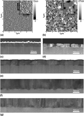
Figure 1 shows the atomic force microscopy (AFM) and HAADF STEM images of the AlN NL grown using different growth modes and conditions. Their analysis reveals the increasing average lateral grain size in the films nucleated by the standard PA MBE at substrate temperatures raising from T S ∼ 550 °C up to the maximum attainable value of T S ∼ 785 °C and transition from the standard PA MBE mode to the MEE one [Figs. 1(a) and 1(b)], with the maximum width reaching even 100 nm.
AFM images illustrating different grain dimensions in NLs grown at the (a) low substrate temperature (T S = 550 °C) and (b) high substrate temperature (T S = 785 °C) by MEE. HAADF STEM images of 25-nm-thick AlN NLs grown on the c-Al2O3 substrate by (c) conventional PA MBE at T S = 550 °C, and (d) T S = 780 °C as well as by MEE at T S = 780 °C using different time of the Al flux supplying per MEE cycle: (e) t Al = 15 ML, (f) t Al = 6 ML and (g) t Al = 3 ML. The two latter images were made for the thick AlN buffer layers.

These data confirm the results of our previous studies of AlN NLs by atomic force microscopy and conventional TEM, Reference Nechaev, Aseev, Jmerik, Brunkov, Kuznetsova, Sitnikova, Ratnikov and Ivanov2,Reference Ivanov, Nechaev, Sitnikova, Ratnikov, Yagovkina, Rzheutskii, Lutsenko and Jmerik7 where the steep reduction of the TD density through increasing the grain size and decreasing the grain boundaries length in the films nucleated by MEE has been demonstrated for the first time. In this study, another aspect influencing the roughness of the interface between the AlN NL and the c-sapphire substrate is considered.
Figure 1 demonstrates also the perfect planar AlN/c-Al2O3 interfaces for the NLs grown by the standard PA MBE at both low and high substrate temperatures [Figs. 1(c) and 1(d)]. The interface flatness was dramatically disturbed in the films grown by MEE [Figs. 1(e) and 1(f)]. The step-like roughness of this interface can reach the depths in the sapphire substrate of ∼5 nm in the case of the maximum nominal thickness of Al (t Al = 15 ML) supplying per one MEE cycle [Fig. 1(e)]. However, the morphology of the interface could be somewhat improved at the shorter Al pulse (t Al = 3–6 ML) [Fig. 1(g)]. Further comparative XRD study of the heterostructures grown at the different MEE parameters revealed the higher structural quality (lower average TD density) of the AlN films grown at the shorter durations of Al MEE pulses (t Al = 3–6 ML).
The complex nature of the AlN/c–Al2O3 interface cannot be explained by the HT diffusion of oxygen atoms from the substrate into the growing AlN layer as was done to explain the voids formed at the same interface during the HT MOCVD of AlN films on sapphire. Reference Miyagawa, Yang, Miyake, Hiramatsu, Kuwahara, Mitsuhara and Kuwano12 Considering the relatively low growth temperatures of the PA MBE (T S < 800 °C) and the planar interfaces in the AlN NLs grown by the standard MBE at the LTs and HTs [Figs. 1(c) and 1(d)], one can assume that the observed step-like interface roughness most probably originates during the several first cycles of the MEE growth of NL, when the pure metallic Al with the high enough deposition doze of 6–15 ML may interact with the c-Al2O3 substrate in between the AlN nuclei.
To describe the interaction between Al microdroplets and sapphire substrates at the temperatures above the Al melting point (660 °C), which result in formation of the rough interface, Levi and Kaplan Reference Levi and Kaplan13 proposed two mechanisms: (i) epitaxial growth of α-Al2O3 compound due to the molten Al oxidation at the interface and (ii) dissolution of the sapphire substrate by the molten Al with formation of the gaseous oxide Al2O through the reaction: 4Al(l) + Al2O3(s) = 3Al2O(g). Reference Champion, Keene and Silwood14 The former mechanism dominates at low substrates temperatures, while the latter becomes prevailing at HTs, with the boundary temperature being as high as 1100 °С, which is definitely higher than that used by us in PA MBE. However, under the ultrahigh vacuum conditions with extremely low residual oxygen pressure, inherent for MBE, only the dissolution mechanism works while the oxidation one seems to be ineffective. Therefore, it is necessary to explain how can the dissolution work at the lower temperature used in our experiments (∼800 °C). Indeed, the critical temperature of dissolving the sapphire by the Al droplets can be reduced down to ∼900 °C, Reference Zhou and De Hosson15 which was confirmed later by the independent studies. Reference Ksiazek, Sobczak, Mikulowski, Radziwill and Surowiak16 The possibility of further reducing the critical temperature with decreasing the size of Al droplets was also mentioned. The growth of a metallic thin film in accordance with the general theory begins from the formation of the nucleation droplets with nanoscale dimensions and density, which are determined by the substrate temperature. Therefore, one can expect quite noticeable interaction of the pure metallic Al nanoparticles with the sapphire at the relatively LTs. In addition, the presumably defect-free AlN NL grains formed by the MEE technique can induce the strong elastic stresses to the sapphire substrate at the grain boundaries. This may also shift the above dissolving reaction to the PA MBE temperatures due to contribution of the strain-induced Gibbs free energy, which usually reduces the formation enthalpy of a solid-state component. Reference Ivanov, Altukhov, Argunova, Bakun, Boudza, Chaldyshev, Kovalenko, Kop'ev, Kutt, Meltser, Ruvimov, Shaposhnikov, Sorokin and Ustinov17
The excessive elastic stress in the AlN nuclei during the MEE growth is confirmed by the comparison of XRD data obtained for 390-nm-thick AlN buffer layers grown on the different NLs, as shown in Table I. It demonstrates the significant residual compressive stress and the small curvature radius (negative) in the AlN layer containing the MEE NL, contrary to the two other layers nucleated in the conventional MBE mode, which are nearly stress-free. Indeed, it has been well established that the merging of the initial AlN nuclei leads to arising the tensile stress in the AlN/Al2O3 film due to the bonding atoms from the neighboring grains. Reference Radhavan and Redwing18 The difference in the thermal expansion coefficient between AlN and sapphire results in compensation of the tensile stress during the wafer cooling. But if the original AlN nucleation islands are highly compressively strained and defect-free, as suggested for the MEE case, the continuous as-grown film becomes strain-free or just slightly tensile-strained at the growth temperature, and hence, strongly compressively strained after cooling down. Moreover, the tensile coalescence stress is inversely proportional to the grain diameter, Reference Nix and Clemens19 which also reduces a probability for the stress in the HT MEE nucleated film to be converted from compressive to tensile during growth. In contrast, the layers with LT NL, having the smaller size of nucleation grains, possess the higher tensile coalescence stress and smaller internal compressive stress inside the nuclei, which results in the highest tensile stress during growth and the lowest residual compressive stress after cooling in good agreement with our experimental data (Table I).
XRD data obtained on 390-nm-thick AlN buffer layers for different NLs.

Finally, it should be noted that despite the strong interaction between Al metal and the substrate during the first several cycles of MEE of the AlN NL on sapphire and some deterioration of the AlN/c–Al2O3 interface, the following growth of this layer up to the thickness of about 50 nm leads to formation of the homogeneously elongated grains with the atomically flat surface and strongly lowered TD density as shown in Fig. 1(g) and in our previous studies. Reference Nechaev, Aseev, Jmerik, Brunkov, Kuznetsova, Sitnikova, Ratnikov and Ivanov2,Reference Ivanov, Nechaev, Sitnikova, Ratnikov, Yagovkina, Rzheutskii, Lutsenko and Jmerik7 The comparative XRD study of the special test 390-nm-thick AlN buffer layers with different NLs (two right columns in Table I) confirmed the best quality for the films grown on MEE NLs (especially for those using smaller Al deposition amount per MEE cycle—3–6 ML) and these regimes were used in the most growth runs of the QW heterostructures studied in this paper.
B. Reduction of the TD density in AlN/GaN buffer structures on c-Al2O3
The XRD data analysis and the in situ quantitative monitoring of the RHEED patterns distance revealed a strong elastic stress variation during the growth of the 2D-AlN MME buffer layer when 2D or 3D ultrathin GaN interlayers of different thickness (3–6 nm) and growth conditions (N- or Ga-rich) were inserted. The Ga-rich 2D-GaN interlayers usually remained pseudomorphic, which resulted in the generation of the additional compressive stress in the AlN buffer, leading to the film detachment from the substrate with increasing the number of the interlayers. In contrast, the N-rich GaN interlayers exhibited nearly full relaxation of their lattice constant to the bulk value, which raised tensile stress in the following AlN buffer, resulting in the film cracking at a large number of such interlayers or reduced distance between them. This indicates the complexity of the generation and relaxation of the elastic stress in the heterostructures. Thus, the detailed study of the stress evolution during PA MBE of the AlN films with the GaN interlayers on c-Al2O3 substrates by using in situ measurements of the wafer curvature will be reported elsewhere.
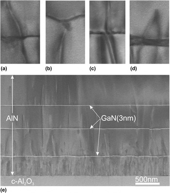
From the TD filtering point of view, the 3-nm-thick GaN interlayers grown under the moderate N-rich stoichiometric conditions were found to have optimal parameters that suppressed the propagation of the TDs and preserved the AlN buffer layer from cracking and detaching. The partial relaxation of the compressive stress in the interlayers generated misfit dislocations in a basal plane at the GaN/AlN interfaces. The dislocations interacted with the TDs having the same Burgers vectors and caused their redirection in a basal plane (blocking effect) or bending direction followed by their annihilation and/or fusion as demonstrated in our previous study. Reference Ivanov, Nechaev, Sitnikova, Ratnikov, Yagovkina, Rzheutskii, Lutsenko and Jmerik7 Figure 2 illustrates these elementary processes observed in the samples under study and the general filtering effect in AlN buffer layer with the several GaN interlayers. It is also seen from Fig. 2 that the first GaN interlayer is the most efficient for decreasing the TD density, and thereafter, the TD-filtering effect is somewhat reduced.
TEM images illustrating the main elementary processes governing the behavior of TDs in the partially strained 3 nm-GaN/AlN multilayer buffer heterostructures: (a) bending, (b) redirection, (c) fusion, and (d) annihilation. (e) A general HAADF STEM view of the cross-section of the AlN buffer layer of one structure, illustrating the filtering effect of the GaN interlayers.

Generally, the efficiency of the GaN interlayers as blockers of TDs depends on numerous parameters, such as their thickness, morphology, number, and on morphology of the AlN layers grown between them. To date, our narrowest FWHM values of XRD reflexes were measured in the 2-μm-thick AlN films with the HT MEE-grown NLs and 2D-AlN buffer layer in which six equidistant 3-nm-thick 3D-GaN interlayers grown at the moderate N-rich conditions were inserted. The measured values of 570 and 600 arcsec for XRD ω-rocking curves for symmetrical (0002) and skew-symmetrical
 $\left( {10\bar 15} \right)$
AlN reflexes, respectively, correspond to the screw and edge TD densities of ∼7 × 10⁸ and ∼2 × 109 cm−2, respectively.
C. HR TEM visualization and PL properties of AlGaN-based QW grown by SDA within the AlGaN waveguide
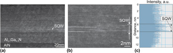
Figure 3 shows the HAADF STEM images of the SQW structures comprising the 90-nm-thick Al0.7Ga0.3N barrier layer grown under the metal-rich conditions (the flux ratio III/N ∼ 2.8) at T S = 700 °C and the well of the nominal thickness of 2.5 nm and the Al molar concentration of 60%, grown by SDA technique using three nominally 0.7-ML-thick GaN insertions. These images revealed the presence of 1–2 ML-thick Ga-enriched AlGaN disks embedded into the AlGaN barrier possessing a slightly higher Al content. Indeed, the contrast of the HAADF STEM images is sensitive to the composition of the sample (so called Z-contrast), i.e., the atomic columns that contain more elements of larger atomic mass (such as Ga) appear brighter on the high-resolution HAADF STEM images due to the higher electron scattering [Figs. 3(a) and 3(b)]. The disks in the QW region seem to be spatially distributed in the growth direction in accordance with the sequential modulations of the Al-flux during SDA growth [Fig. 3(b)]. To better visualize the compositional variations in the growth directions, we digitally integrated the intensity of the atomic columns along the lateral direction in Fig. 3(b) and plotted it in Fig. 3(c), which clearly demonstrates the presence of the Ga-enriched regions in the SQW.
(a, b) HAADF STEM images of 2 nm-Al0.6Ga0.4N/Al0.7Ga0.3N SQW formed by SDA with the three nominally 0.7-ML-thick GaN insertions taken with different resolutions. Figure (c) corresponds to the high-resolution TEM image (b) and illustrates the intensities of atomic columns, which were digitally integrated in the lateral direction.

These (1–2)-ML-thick Ga-enriched AlGaN islands formed in the SDA-QW could presumably play a role of carrier localization sites and also reduce the quantum-confined Stark effect (QCSE) in the QW region. To confirm these assumptions, we performed detailed temperature-dependent PL and TR PL studies of SDA DQWs possessing the same thicknesses (3 and 7 nm) and differing in the number of SDA superlattice periods (see the DQW sample description in the experimental part).
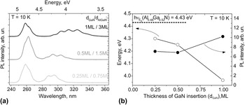
Figure 4 shows the LT PL spectra of the three SDA AlGaN DQW structures, as well as the dependence of the central wave length of their QW-related PL band and its PL integral intensity on the thickness of the GaN insertions in the SDA regime used (d GaN). With decreasing d GaN, the longer wave length PL band, ascribed to the emission from DQW, becomes narrower [Fig. 4(a)] and shifts to shorter wave lengths, approaching the value corresponding to the energy gap of the bulk Al0.48Ga0.52N layer grown at continuous fluxes [Fig. 4(b)]. Reference Jmerik, Shubina, Mizerov, Belyaev, Sakharov, Zamoryanskaya, Sitnikova, Davydov, Kop’ev, Lutsenko, Danilchyk, Rzheutskii, Yablonskii and Ivanov5 The heterostructure with the largest d GaN exhibits the highest integral PL intensity of the QW PL band.
(a) PL spectra of the heterostructures with AlGaN QW grown at different d GaN; (b) QW PL band spectral position and integrated intensity as functions of d GaN; horizontal line indicates the energy gap value for Al0.48Ga0.52N grown under continuous fluxes.

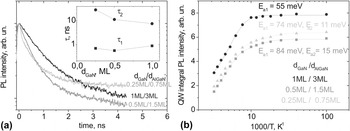
The time- and temperature-dependent QW PL intensities are shown in Fig. 5. All the PL decay curves [Fig. 5(a)] demonstrated a two-exponential decay. The behavior of the faster PL decay component τ1 with d GaN [inset of Fig. 5(a)] is similar to that of the integral PL intensity. Therefore, one can conclude that τ1 is determined mainly by the influence of nonradiative recombination centers. The slower time component τ2 decreases with d GaN increasing being one order of magnitude larger than τ1. The heterostructures with QWs grown at d GaN = 0.25 and 0.5 ML exhibit the steeper temperature quenching of the PL intensity compared to the one grown with d GaN = 1 ML. Although the total reduction of the integral PL intensity from 10 to 300 K is similar for all the structures, it does not exceed 60%. In contrast to the SDA QWs grown with d GaN = 1 ML, where the single PL activation energy E a = 55 meV was observed, two channels were detected for two others SDA DQW structures with E a1 and E a2 of 15, 84 and 11 meV, 74 meV, respectively [Fig. 5(b)].
(a) QW PL kinetics. Inset shows dependencies of the decay time values on d GaN. (b) Temperature versus QW PL intensity. The activation energies of nonradiative recombination centers were determined according to the Arrhenius model.

The observed PL data could be explained in the following way. In the DQW structures grown by SDA with d GaN < 1 ML, the lower PL efficiency, the steeper PL temperature quenching, and the shorter wave length PL emission can be explained by more homogeneous alloy of the QW layer, the smaller localization energy of photogenerated carriers, and their faster escape to the nonradiative recombination centers with temperature rising. The weaker localization causes also the stronger QCSE resulting in the larger τ2 component of the PL kinetics. In contrast to that, the deeper localization and stronger spatial confinement of photogenerated carriers in the states related to the GaN insertions with d GaN = 1 ML in the respective SDA QW lead to the higher PL efficiency, the slower PL temperature quenching, and the suppression of the QCSE, which results in lower τ2. However, the PL300 K/PL10 K intensity ratio cannot be used directly for estimation of the IQE of the structures because it does not take into account the nonequilibrium carrier transport in the barriers, which is influenced noticeably by the phenomena addressed in the following sections.
D. Formation of local barriers in AlGaN waveguide layers grown by using DETA technique
In addition to the QW morphology, the HAADF STEM image in Fig. 3(a) exhibits the thin darker stripes of higher Al content, which could be caused by AlGaN growth on the overheated surface in the TME process used for excessive Ga elimination from the Al0.70Ga0.30N layer surface during growth interruptions. After short-term surface annealing for Ga desorption by closing the main shutter, the growth of this sample was recommenced immediately by opening the shutter while the substrate temperature remained sufficiently high during its ramping from 740 to 700 °C for approximately 10 s. Thus, the incorporation of Ga into the AlGaN layer was reduced, which led to the formation of the thin Al-enriched barrier layers that may impede nonequilibrium carrier transport toward a SQW. This assumption was confirmed by PL studies with no evidences of stimulated emission even at the relatively high optical power density up to I exc ∼ 5 MW/cm2, while the SQW structures embedded in the AlGaN waveguide layer grown by standard PA MBE and having no internal barriers demonstrated stimulated emission at moderate I exc = 300–500 kW/cm2. Thus, the transport of charge carriers in the waveguide layer in the directions normal to the SQW plane strongly affects the excitation of stimulated emission in the laser heterostructures. Therefore, the growth procedure should avoid the formation of such additional Al-enriched AlGaN barriers layers, which can be achieved, for example, by closing the metal flux shutters during the substrate temperature stabilization (∼10 s) after opening the main shutter in the TME cycle.
E. Spontaneous composition modulation in AlGaN layers grown by PA MBE at metal-rich conditions
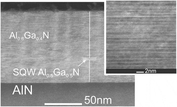
Figure 6(a) shows HAADF STEM images of the AlGaN-based laser structure consisting of a 90-nm-thick Al0.6Ga0.4N waveguide layer grown under strongly metal-rich conditions with the flux ratio III/N = 1.7 at T S = 690 °C. The Al0.5Ga0.5N SQW with a nominal thickness of 2 nm was formed using the SDA technique. The waveguide layer exhibits relatively large spontaneous compositional modulation in the growth directions such that the artificial SQW is hardly distinguishable. Such SQW structures with the AlGaN barrier composition in the range of x = 0.6–0.7 and just a 10% difference in the Al mole fraction between the barrier and QW AlGaN alloys usually demonstrate a single PL line where the deep localization states in the barrier, caused by its strong compositional fluctuations, merge with the localized states in the QW. Although it is difficult to distinguish the SQW PL band in the continuous wave (cw) PL spectra, the TR PL measurements revealed that the barrier emission related to the higher energy states in the PL band essentially decays during 100–200 ps, whereas the QW emission (longer wave length side) possesses the decay time of about 400 ps, which is insensitive to both emission wave lengths within the PL band and temperature (up to 300 K). Reference Shevchenko, Toropov, Nechaev, Jmerik, Shubina, Ivanov, Yagovkina, Pozina, Bergman and Monemar20 Due to strong localization effects in the QW structures, they exhibited rather high IQE of the integral PL emission (∼25%), measured as the ratio between room temperature and LT PL integral intensities at a low excitation level. However, the observed stability of the QW emission decay with temperature suggests that the quantum efficiency of the QW emission alone can be even higher. This phenomenon requires more detailed investigation.
HAADF STEM images of the Al0.6Ga0.4N waveguide layer with the embedded 2-nm-thick Al0.5Ga0.5N SQW (insertion shows a magnified image of the waveguide layer).

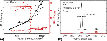
Despite the fluctuating composition profile, the structure demonstrated a reasonable level of the threshold power density (I thr) of 350 kW/cm2. The stimulated emission, which is determined from the dependencies of edge emission intensity and its FWHM value on the excitation power density, as shown in Fig. 7(a). Figure 7(b) demonstrates the transverse electric (TE) and transverse magnetic (TM) emission spectra from the cleaved edge of the heterostructure operating at the excitation power density exceeding twice the threshold.
(a) FWHM of the PL peak and its intensity for different pumping power densities, measured from the edge of the Al0.5Ga0.5N/Al0.6Ga0.4N SQW heterostructure at room temperature. (b) TE- and TM-polarized emission spectra measured at the same excitation power density I exc = 2I thr.

Additional studies are necessary to find the physical origin of the spontaneous Al-content modulation described above and its influence on the characteristics of spontaneous and simulated UV emissions from AlGaN QW heterostructures with compositionally inhomogeneous barrier layers.
III. CONCLUSIONS
The structural properties of AlGaN-based SQW heterostructures grown by PA MBE on the standard c-Al2O3 substrates have been studied by HAADF STEM and XRD. Optimal growth conditions for the AlN NL and ultrathin GaN interlayers have been found, which lowered the TD densities down to ∼7 × 10⁸ and ∼2 × 109 cm−2 for screw and edge ones, respectively. The step-like roughness of the AlN/c–Al2O3 interface observed by HAADF STEM for the AlN NLs fabricated by MEE at large enough amount of Al (6–15 ML) deposited per one MEE cycle was proposed to originate from the interaction between molten Al and a c-sapphire substrate during the first several MEE cycles. A quantum disk-like structure of QWs formed by the SDA technique has been confirmed by HAADF STEM. Decreasing the period of the SDA modulation from 4 to 1 ML at the constant well-to-barrier thickness ratio and the QW thickness results in less pronounced carrier localization effects, which lead to the lower PL efficiency, stronger PL temperature quenching, and QCSE. Dependences of UV-stimulated emission parameters on different compositional inhomogeneities in AlGaN waveguide layers grown by both standard and pulsed TME techniques under the metal-rich stoichiometrical conditions have been investigated.
ACKNOWLEDGMENTS
The authors from the Ioffe Institute are grateful to Russian Science Foundation Project #14-22-00107 for the support of the work. Authors are thankful also to Notre Dame Integrated Imaging Facility for support of TEM studies.