1. INTRODUCTION
Since Manz et al. (Reference Manz, Graber and Widmer1990) published the landmark paper on miniaturized total analysis system, researches on chip-based microfluidic systems or micro–total analysis system (µ-TAS) have increased tremendously, much like the revolution in the electronic industry after the invention of transistor and integrated circuit (Pihl et al., Reference Pihl, Sinclair, Karlsson and Orwar2005). The recent trend toward the use of polymeric substrates has been primarily driven by the fact that these materials are less expensive and more adapted to mass–production techniques than silica-based substrates. Polymers have assumed the leading role as substrate materials for microfluidic devices in the recent years (Becker & Gärtner, Reference Becker and Gärtner2008; Mijatovic et al., Reference Mijatovic, Eijkel and Van Den Berg2005). However, there still exists an issue of material incompatibility that needs to be addressed. Polymeric channels, valves, and pumps tend to react with organic solvent samples and cause contamination and device degradation (Gould, Reference Gould2004). Silica-based microfluidic circuits are still considered to be more suitable for applications involving use of strong chemicals.
Currently, microfluidic devices are mainly fabricated by photolithography and soft-photolithography, which involve numerous steps including mask making, mold fabrication, deposition, exposure, and chemical etching. Other replicating techniques by use of master molds are also quite mature and suitable for mass production of polymer-based microfuidics. However, they are time-consuming and expensive processes requiring alignment, stacking, bonding, and assembly of the individual microcomponents (Kikutani et al., Reference Kikutani, Horiuchi, Uchiyama, Hisamoto, Tokeshi and Kitamori2002). It is preferable to develop new techniques for rapid fabrication in a single procedure.
Laser-based techniques are highly attractive for flexible and high-speed manufacturing compatible with a high level of integration of each component (Sugioka et al., Reference Sugioka, Cheng and Midorikawa2007; Khan Malek et al., Reference Khan Malek2006). Photostructurable glasses such as Foturan are interesting materials for µ-TAS or lab-on-chip, as they are inherently photosensitive, and hence do not require a photoresist layer for patterning (Dietrich et al., Reference Dietrich, Ehrfeld, Lacher, Kramer and Speit1996; Becker et al., Reference Becker, Arundell, Harnisch and Hülsenberg2002). Attempts has been made to study laser machining of Foturan glass (Brokmann et al., Reference Brokmann, Jacquorie, Tberg, Harnisch, Kreutz, Hülsenberg and Roprawe2002; Livingston & Helvajian, Reference Livingston and Helvajian2005; Stillman et al., Reference Stillman, Judy and Helvajian2008); however, the researches were carried out using ns ultraviolet (UV) laser instead of ultrashort infrared (IR) laser. Those researches focused on surface machining only because ns UV laser is highly absorbed at surface of glass and thus not suitable for subsurface machining. The current study aimed to explore use of ultrashort IR laser for subsurface machining. Foturan glass is transparent at IR wavelengths, so IR laser can be used to irradiate the interior of the glass. However, in case of ns IR laser, the laser energy is absorbed little by the glass because of the linear absorption mechanism. A fs laser pulse can produce an electric-field strength that approaches or exceeds the strength of the electric field that holds valence electrons in a transparent material to their ionic cores (Gamaly et al., Reference Gamaly, Rode, Luther–Davies and Tikhonchuk2002). In this regime, the interaction between the laser pulse and the material at the focal point becomes highly nonlinear, leading to a local photomodification in the material (Davis et al., Reference Davis, Miura, Sugimoto and Hirao1996).
This absorption mechanism, with non-adiabatic cluster expansion in ultrashort laser interaction (Yu et al., Reference Yu, Yu, Xu, Tian, Chen and Wong2007) and the intense local plasma heating (Faenov et al., Reference Faenov, Magunov, Pikuz, Skobelev, Giulietti, Betti, Galimberti, Gamucci, Giulietti, Gizzi, Labate, Levato, Tomassini, Marques, Bourgeois, Dobosz, Ceccotti, Monot, Reau, Popescu, D'oliveira, Martin, Fukuda, Boldarev, Gasilov and Gasilov2008), makes it possible to carry out photomodification inside the glass at the focal spot of fs IR laser (Davis et al., Reference Davis, Miura, Sugimoto and Hirao1996; Fernandez et al., Reference Fernandez, Hegelich, Cobble, Flippo, Letzring, Johnson, Gautier, Shimada, Kyrala, Wang, Wetteland and Schreiber2005; Lam et al., Reference Lam, Tran and Zheng2007; Kasperczuk et al., Reference Kasperczuk, Pisarczyk, Kalal, Martinkova, Ullschmied, Krousky, Masek, Pfeifer, Rohlena, Skala and Pisarczyk2008; Bagchi et al., Reference Bagchi, Kiran, Bhuyan, Bose, Ayyub, Krishnamurth and Kumar2008). Direct fabrication of a three-dimensional (3D) microstructure inside transparent glass using fs laser offers great potential for the manufacture of 3D integrated microchips without the need for the cumbersome alignment and assembly processes of individual components.
Direct fabrication of individual microfluidic channels has been demonstrated inside fused silica (Marcinkevičius et al., Reference Marcinkevičius, Juodkazis, Watanabe, Miwa, Matsuo, Misawa and Nishii2001; Bellouard et al., Reference Bellouard, Said, Dugan and Bado2004; Hnatovsk et al., Reference Hnatovsk, Taylor, Simova, Rajeev, Rayner, Bhardwaj and Corkum2006). However, fused silica presents much less efficiency and lower through–put in manufacturing compared with photosensitive glasses such as Forturan glass (Sugioka et al., Reference Sugioka, Cheng and Midorikawa2005). Photosensitive glasses also possess added advantage over fused silica in that heat treatment may be carried out to smoothen surfaces of microstructures through transformation to a glass ceramic (Cheng et al., Reference Cheng, Sugioka, Midorikawa, Masuda, Toyoda, Kawachi and Shihoyama2003). The ability to directly form 3D microstructures in Foturan glass using lasers, together with its resistance to high temperature and corrosion, as well as high optical transparency, have made Foturan glass particularly attractive as a platform for the bioanalysis microdevices (Becker et al., Reference Becker, Arundell, Harnisch and Hülsenberg2002; Sugioka et al., Reference Sugioka, Cheng and Midorikawa2005; Fisette & Meunier, Reference Fisette and Meunier2006; Wang et al., Reference Wang, Sugioka and Midorikawa2008).
However, many issues related to fs laser subsurface micromachining are poorly understood, including effects of fs laser irradiation on size of microfluidic channel and achievable structural aspect ratio, which is defined as the ratio of depth to width of the channel. Of particular interest is the study of fs laser induced crystallization in Foturan glass. As hydrofluoric acid (HF) preferential etching process depends on the transformation of the glass from amorphous phase to crystalline structure, the major factors affecting the glass crystallisation process were investigated with regards to the fs laser process, and the post thermal annealing process in this study. Special effort was made to produce different configurations of microfluidic chambers and channels to demonstrate that fs laser can be successfully used for rapid fabrication of 3D microfluidic structures inside the photosensitive glass without the need to assemble the individual components.
2. EXPERIMENTAL
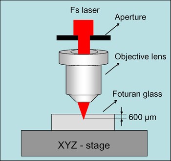
Foturan glass was used in the study. It is a photosensitive glass composed of lithium aluminosilicate doped with trace amounts of silver, cerium, sodium, and antimony (Dietrich et al., Reference Dietrich, Ehrfeld, Lacher, Kramer and Speit1996). A Ti:sapphire regenerative amplifier fs laser system (CPA2001 Clark–MXR) emitting pulses at repetition rate of 1 kHz with a wavelength of 775 nm was used in the direct writing experiments. Pulse energy was adjusted over a range of 0.1 to 4.0 µJ using polarizer and neutral density (ND) filters. The focusing system was a 50× objective lens with a numerical aperture (N.A.) of 0.55. A 3 mm aperture was placed before the objective lens to block the outer part of the original output beam so as to improve the beam quality, as shown in Figure 1. The laser beam was kept stationary, but the sample was moved at speeds of 0.1 to 1.5 mm/s on a PC-controlled motorized XYZ stage.
(Color online) Illustration of experimental setup used for fs laser subsurface micromachining.

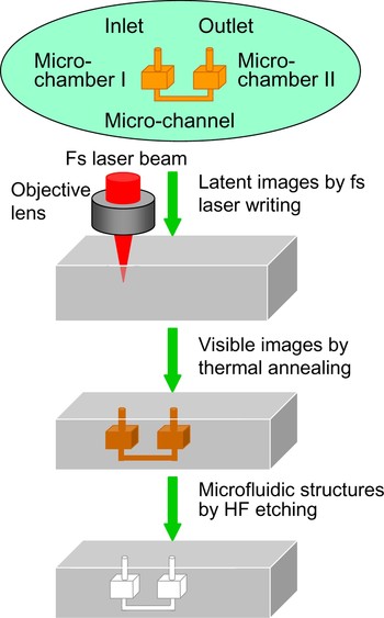
The fabrication procedure of microfluidic channels includes three steps: (1) Drawing latent images of microfluidic structures inside the glass by scanning a tightly focused fs laser beam; (2) Thermal annealing (the temperature was first ramped up to 500°C at 5°C/min, held at this temperature for 1 h, raised to 605°C at 3°C/min and then held for another hour); and (3) Etching at room temperature in a solution of 10% HF diluted with water in an ultrasonic bath. An example is given later in Figure 10 to illustrate the processes of fabrication.
Raman Renishaw RM1000 microspectrometer with a He-Ne laser at 633 nm as the excitation source (Renishaw plc, UK) was used to identify the glass structure crystallization within the laser irradiated areas.
3. RESULTS AND DISCUSSION
3.1. Microstructure Crystallization
The ability to fabricate microfluidic structures inside the glass relies upon the formation of microhollow structures by selectively etching away the crystallized parts in HF solution. Therefore, the major factors affecting the glass crystallization process have to be studied with regards to the fs laser writing process and the subsequent annealing process.
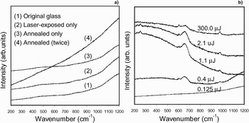
Figure 2 shows the micro–Raman spectra of samples obtained under various laser writing parameters and thermal treatments. Raman spectroscopy is a light scattering technique for diagnosing the internal structure of molecules and crystals. In the current light scattering experiment, light of a known frequency of 633 nm was scattered from the fs laser irradiated samples, and then the scattered light was analyzed for frequency. Raman scattered light is frequency–shifted with respect to the excitation frequency and the “Raman shift” is an intrinsic property of the structure of material. It can be seen from Figure 2a that no peaks appeared in the Raman spectra for the original glass, fs laser irradiated glass, or thermally annealed glass. This indicates that structure of the original Foturan glass is amorphous and the structure remained amorphous when either only laser direct writing process or only thermal annealing (either once or twice) was applied to the sample. It is very interesting to observe from Figure 2b that thermal annealing after fs laser exposure resulted in crystallization (as indicated by the Raman peaks), although neither laser exposure alone or anealling alone could crystallize the amorphous structure. The peaks around wavenumbers of 979.7 cm−1, 659.7 cm−1, 603.7 cm−1, and 254.6 cm−1 in Raman spectra in Figure 2b were identified to correspond to crystallites of lithium metasilicates (Li2SiO3) (Richet et al., Reference Richet, Mysen and Andrault1996). The study revealed a laser pulse energy threshold for crystallization. As shown in Figure 2b, when the energy was less than 0.125 µJ (corresponding to a measured laser fluence of 0.64 J/cm2), no glass crystallization was observed even after annealing.
Micro-Raman spectra showing (a) amorphous structures after laser-exposure alone or thermal annealing alone, (b) crystallization in samples annealed after laser-exposure (laser scanning speed 0.5 mm/s).

3.2. Geometric Control of Microchannels
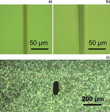
Glass pieces with a size of 10 mm by 10 mm and thickness of 2 mm were used in the laser experiment. Fs laser direct writing was carried out from one end surface to the other to draw microfluidic channels at 600 µm below the top surface of the Foturan glass (Fig. 1). Figure 3 shows some examples of channels successfully produced using laser energy of 1.1 µJ at speed of 1.5 mm/s. It is noted that the energy used is well above the threshold energy for crystallization, which is 0.125 µJ as shown in Figure 2b.
(Color online) Optical micrographs showing (a) top view of microfluidic channel directly written with fs laser at 600 µm below surface, (b) top view of the channel after thermal annealing and HF etching for 10 min, and (c) cross-sectional view of a microchannel entrance after thermal annealing and etching for 20 min.

The microchannel in Figure 3b is observed to be tapered. The tapered shape was found to be related to the chemical etching process. Etching always started from the part of channel in direct contact with HF and then moved inside gradually, resulting in progressively shorter etching time and thus smaller channel size for the part of channel exposed to HF at later stage.
Cross–sections of the microchannels were studied and found to be elongated along the direction of laser beam propagation, as shown in Figure 3c. This elongated shape is mainly derived from the longitudinal distribution of the spatial intensity of the focused beam. When the material is exposed to fs laser, the refractive index is locally modified within an ellipsoidal shape whose size is defined by the N.A. of the optical system and by the laser parameters such as beam waist and energy (Wang et al., Reference Wang, Sugioka and Midorikawa2007a).
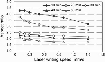
The elongated shape may be a big advantage for some applications, but it may have to be tuned for some other applications. The value of structural aspect ratio typically ranges from 1.7 to 4.3 under the conditions of laser scanning speed of 0.1 to 1.5 mm/s, laser energy of 0.4 to 2.1 µJ, and HF etching time of 10 to 50 min. Figure 4 shows that the structural aspect ratio can be tuned by adjusting scanning speed and etching time.
Effect of laser writing speed and HF etching time on structural aspect ratio of the channel entrance.

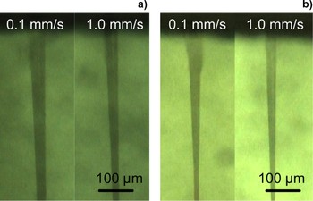
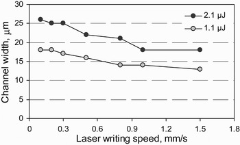
Figure 5 shows some typical images of the embedded microfluidic channels faricated using different writing parameters and etched in HF solution for the same time of 10 min. The channel size becomes smaller with decreasing laser energy and increasing scanning speed. The width of the channel was measured from the smallest section and is shown in Figure 6 as a funtion of laser energy and writing speed.
(Color online) Optical micrographs showing embedded microfluidic channels produced using different laser writing parameters. (a) Energy of 2.1 µJ; (b) smaller energy of 1.1 µJ.

Effect of laser energy and speed on microfluidic channel width.

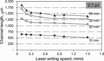
Microchannel length was also measured and is shown in Figure 7 to decrease with either increasing laser scanning speed or increasing etching time. When laser scanning speed increases, laser irradition time reduces, making microstructure crystallization more difficult during the subsequent annealing treatment. As etching time increases, the channel becomes longer, resulting in slower material removal.
Effect of HF etching time on microfluidic channel length at various writing speeds.

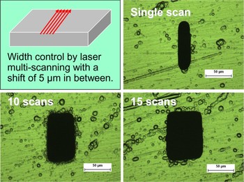
In general, microfluidic components, although often called microchips, are not so small as cell phone or computer chips. For reasons of easy manual handling and in order to combine multi-functions on the same component, the chips are generally not smaller than a few square centimeters (Gottschlich, Reference Gottschlich2004). The width of channels presented in Figure 6 ranges from 13 to 27 µm. It is quite narrow for typical µ-TAS applications where the channel width is usually larger than 50 µm. Figure 8 shows the controlling of the channel width by multi-scanning the laser beam horizontally at a pitch of 5 µm. The channel width can be easily adjusted by laser beam multi–writing. Meanwhile, the cross-sectional profile of the microchannel is easily tunable from elliptical to rectangular so as to meet the different requirements of microfluidic channels.
(Color online) Increasing channel width through multi-scanning of the laser beam with a pitch of 5 µm (the white numbers indicate number of laser scan).

3.3. Surface Smoothening Through Secondary Annealing
Since the crystallites of the lithium meta-silicate must be developed by the heat treatment to form a connected etchable network (Helvajian et al., Reference Helvajian, Fuqua, Hansen and Janson2001), the removal of the crystallites by etching leaves a coral-like surface morphology behind. This surface may adversely affect the reagent flow in the microchannel. Therefore, effort was made to smoothen the surface through secondary thermal annealing after chemical etching.
The channel width in the range of several tens of µm is too small for the purpose of measuring surface roughness using surface profilometer. Therefore, the multi-scanning technique as illustrated in Figure 8 was used to produce a much larger channel with a cross-section of 1.5 mm by 3 mm.
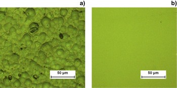
Secondary annealing was carried out by ramping the temperature slowly at a rate of 5°C/min to 570°C, keeping the sample at this temperature for 5 h, and then cooling it in furnace. Afterward, the channel was sectioned along its axis to make its wall surface accessible to a Stylus Profilometer (Taylor-Hobson Form Talysurf Series 2) for carrying out the roughness measurement. Surface roughness R a was found to be reduced significantly by the secondary annealing from 272 nm to 7 nm. The effectiveness of secondary annealing was also confirmed through observation under the optical microscope, as shown in Figure 9.
(Color online) Optical micrographs showing (a) rough surface before secondary annealing, and (b) much smoother surface after secondary annealing.

3.4. 3D Integration of Microcomponents
The same procedure of hollow structure formation can be applied to fabricate microfluidic chambers buried inside Foturan glass. The use of such a fs laser direct subsurface writing enables the true 3D fabrication, as illustrated in Figure 10.
(Color online) Illustration of 3D microfabrication process inside Foturan glass.

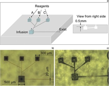
By arranging four cubic chambers serially in the glass, we built a microfluidic reagent mixer and reactor, as shown in Figure 11. The inlet of each chamber was opened at the top surface of the glass, and one outlet was opened at one side facet which was connected to the bigger chamber (mixer or reactor). By computer controlled movement of the glass sample on the XYZ stage, the 3D images of the miro-fluidic structures of chambers and channels were continuously written inside the glass. After thermal annealing and HF etching, the integrated microfluidic structures were rapidly prototyped inside a single glass chip, as shown in Figures 11b–11c. Of interest to note is that the device fabricated contains a channel with a tilted angle, as shown in Figure 11a. It is difficult to produce such tilted channel using other techniques except fs laser direct writing.
(Color online) 3D integration of different chambers and channels for storage and infusion of reagents. (a) schematic of the designed microfluidic structures; (b) after laser subsurface writing and annealing; and (c) after HF etching for 100 min.

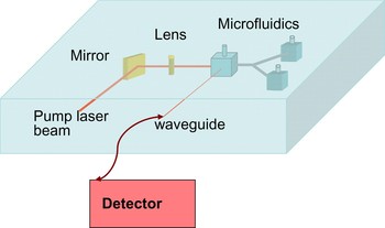
The current study focuses on subsurface micromachining of microfluidic structures. It is noted that fs laser direct writing can also be used to produce optical waveguide (Wang et al., Reference Wang, Sugioka and Midorikawa2007a) and microlens (Wang et al., Reference Wang, Sugioka, Hanada and Midorikawa2007b) inside Foturan glass. Therefore, the direct writing technique makes it possible to integrate micro-optical and microfluidic components into a single chip to highly enhance the functionality and performance of the microchip, e.g., for photonic biosensing, as shown in Figure 12.
(Color online) Sophisticated microdevice integrating micro-optical components with microfluidic components in a single piece of glass for on-site biosensing application.

4. CONCLUSIONS
Amorphous structure of the Foturan glass cannot be crystallized by fs laser irradition alone or heat treatment alone. However, crystallites of lithium metasilicates (Li2SiO3) were found to be formed by thermal annealing of the glass after fs laser exposure above the threshold fluence of 0.64 J/cm2. The crystallized structure can be removed selectively by chemical etching in HF solution. The findings led to a method of subsurface micromachining of microfluidic channels inside Foturan glass using fs laser.
The channel size can be increased by increasing the laser energy or decreasing the laser scanning speed. Channels of width ranging from 13 to 27 µm can be produced easily using single laser scan, and a multi–scanning technique was developed to produce channels or chambers of much larger dimensions.
Effort was made to smoothen the surface of channels produced, and evidence was shown that secondary thermal annealing after chemical etching could reduce the surface roughness R a significantly from 272 nm to as low as 7 nm.
A microfluidic reagent mixer and reactor consisting of four cubic chambers and multiple channels was produced in a single piece of glass to demonstrate the success in rapid 3D fabrication using the fs laser subsurface writing technique.
ACKNOWLEDGMENT
The authors would thank SIMTech for financial support through Project C08–M–042.