Introduction
An interesting chemical discrepancy was noticed that was both amusing and inspiring. On one hand, solid-state chemists widely use binary and ternary phase diagrams when planning their syntheses.Reference Ropp1 On the other hand, I asked many organic chemists if they ever used C-H and C-H-O phase diagrams. The general answer was no. Chemists rarely use such phase diagrams when they work with molecular species (e.g., with organometallic and coordination compounds). What makes solid-state chemistry so different from molecular chemistry? This can be understood if we take into account that the majority of bulk solids are thermodynamically stable phases corresponding to the global minimum of free energy. In contrast, the absolute majority of molecules does not represent the most stable atomic arrangements and can be converted into more stable species (typically CO2, H2O, N2, and other small molecules with strong bonds). This applies to almost all organic molecules. As a result, organic synthesis requires a step-by-step assembly rather than heating of carbon, hydrogen, and oxygen until they react with each other. To build complex molecules, organic chemists do not allow reactants to fully equilibrate and form the most stable products. Instead, they rely on a well-defined hierarchy of energy scales that allow driving from one local energy minimum to the other local minimum following the reaction pathway.Reference Corey and Cheng2 This approach is the heart of the enormous compositional and structural diversity of molecular compounds.
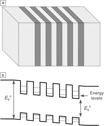
Our research tries to bring these ideas from molecular chemistry into the arena of solids. We were not the first to do so: a good example of non-equilibrium solid is a stack of GaAs-AlAs quantum wells shown in Figure 1. Such a structure can exist only far below the melting points of GaAs and AlAs; if heated, it will equilibrate into a Ga1–xAlxAs alloy. The discovery of semiconductor heterostructures has introduced entirely new ways for electronic structure engineering, enabling exciting device applications and scientific breakthroughs recognized by several Nobel prizes (e.g., Alferov, Kroemer, and Kilby).Reference Stroscio and Dutta3 At the same time, traditional semiconductor heterostructures, grown by vacuum deposition techniques such as molecular beam epitaxy, also have limitations, one being that the electronic structure can be precisely modulated only along one direction, which is the growth direction. As yet, we are unable to provide the same level of control in two- and three-dimensional structures. Another limitation of traditional technology is the cost; quantum well structures are too expensive to use in many consumer products and large area devices such as solar cells.
(a) Stack of quantum wells made of a semiconductor with the bandgap energy E gb showed as dark regions separated with barrier layers made of a semiconductor with the bandgap energy E ga—semiconductor superlattice that allows precise tuning of the electronic structure along the stack direction as shown in panel (b).

We have explored the possibility of building solids where electronic structure can be engineered in all three dimensions; we also focus on the methods that can generate such materials on a “chemical scale,” such as grams or kilograms. Here we learn from molecular chemistry and try to build inorganic solids using step-by-step synthetic routes that enable structural flexibility comparable to that for molecular compounds and polymers. First, we start with simple molecular precursors and synthesize nanoscale modules that will be used as the building blocks for functional solids. Then we assemble these building blocks into macroscopic solids. This approach relies on two different energy scales. The energy scale that holds atoms together inside the building blocks is defined by the energy of chemical bonds. The second energy scale is responsible for assembly of individual building blocks into macroscopic arrays. In this case, we typically rely on the van der Waals and electrostatic forces. One can draw here an analogy with intra- and intermolecular forces in polymers. Finally, one has to come up with a creative surface chemistry that facilitates electronic or magnetic or mechanical coupling between these individual “modules” to form extended electronic states or to develop a collective response to external stimuli.
It is reasonable to ask why we have chosen nanometer scale particles (2–20 nm) as the building blocks for functional solids, instead of something that is smaller or larger. This is because objects that are several-nanometers in size are sufficiently large to develop the key features of the electronic structure of their parent solids.Reference Brus4 To fully understand their behavior, one should take into account quantum confinement phenomena, but there is a good body of knowledge on the physical and chemical properties of such materials.Reference Klimov5 On the other hand, smaller entities such as atomic clusters and large molecules have unique electronic structure and do not follow predictable trends. Building functional materials from inorganic “modules” larger than ca. 100 nm is also difficult, but the problems arise due to gravity and very strong interparticle forces that prevent the formation of ordered assemblies, as discussed later.
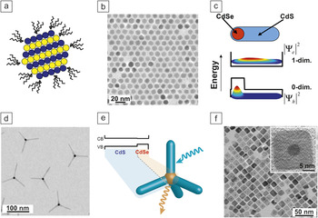
To implement these ideas, we used colloidal chemistry techniques developed during the last decade.Reference Murray, Kagan and Bawendi6–Reference Park, Joo, Kwon, Jang and Hyeon8 Thanks to a large community of excellent scientists who worked on colloidal synthesis of nanomaterials, we now have a well-developed synthetic methodology to make many scientifically and technologically important metals, magnetic materials, and semiconductors in the form of sub-20 nm particles with precisely controlled size and shape (Figure 2). Moreover, each particle can incorporate a heterostructure with several functional components.Reference Cozzoli, Pellegrino and Manna9 It is very common to refer to such sub-20 nm particles as “nanocrystals.” The important common feature of all nanocrystals (NCs) synthesized by colloidal chemistry is the layer of surface ligands (Figure 2a–b) that help to control the size and shape of NCs during synthesis and to disperse NCs in different solvents in the form of easy-to-handle colloidal solutions.
(a) Each nanocrystal has a solid core and a shell of surface ligands that provide stability to colloidal solutions and passivate surface dangling bonds. (b) Surface ligands also provide control over nanocrystal nucleation and growth and allow for the collection of samples with tight size and shape distributions. (c) An example of a nanostructure where an electron and hole have different confinement regimes: the electron and hole with the wave functions Ψe and Ψh are confined in two and three dimensions, respectively. (d–e) Tetrapod-like nano-heterostructures where arms behave as light-harvesting antennas funneling excitation into the central core. (f) Multifunctional nano-heterostuctures with magnetic FePt cores integrated into semiconducting PbS shells. Adapted from References Reference Talapin, Nelson, Shevchenko, Aloni, Sadtler and Alivisatos13, Reference Mueller, Lupton, Lagoudakis, Schindler, Koeppe, Rogach, Feldmann, Talapin and Weller14, Reference Borys, Walter, Huang, Talapin and Lupton16, and Reference Lee, Bodnarchuk, Shevchenko and Talapin17. Note: CB, conduction band; VB, valence band.

Individual building blocks—Nanocrystals
This section covers examples showing the power of modern colloidal chemistry. In the case of semiconductor NCs, the shape of the particle defines the symmetry of electron and hole wave functions.Reference Efros10 For example, in a quantum dot, both electron and hole wave functions are “squeezed” from all directions and are three-dimensionally confined. In a quantum rod, the wave functions are confined in two directions.Reference Hu, Li, Yang, Manna, Wang and Alivisatos11 Some years ago, we synthesized the first structures of what was called “mixed dimensionality.”Reference Talapin, Koeppe, Götzinger, Kornowski, Lupton, Rogach, Benson, Feldmann and Weller12, Reference Talapin, Nelson, Shevchenko, Aloni, Sadtler and Alivisatos13 The conduction and valence band offsets between CdSe and CdS are such that the hole is strongly three-dimensionally confined inside CdSe, whereas an electron can freely move between CdSe and CdS phases being two-dimensionally confined (Figure 2c). By applying an electric field, one can move electrons along the nanostructure and thus change an overlap between the electron and hole wave functions. This introduces a convenient knob to control the electronic structure and radiative recombination rate.Reference Mueller, Lupton, Lagoudakis, Schindler, Koeppe, Rogach, Feldmann, Talapin and Weller14, Reference Kraus, Lagoudakis, Rogach, Talapin, Weller, Lupton and Feldmann15 One can design even more complex structures such as those shown in Figure 2d–e, where a CdSe quantum dot is attached to four CdS rods, behaving as light-harvesting antennas.Reference Talapin, Nelson, Shevchenko, Aloni, Sadtler and Alivisatos13 Such combinations of compositional and morphological engineering with nanometer precision introduces a powerful methodology, which allows chemists to directly manipulate electronic wave functions and carry out charge carrier routing and sub-diffraction focusing of optical fields.
Another example of colloidal nano-heterostructures, where a magnetic FePt core is integrated into a semiconducting PbS shell, is shown in Figure 2f. We explored such nanostructures as the building blocks for materials combining magnetic and semiconducting functionalities, where the inter-component interactions were additionally enforced by tight spatial confinement.Reference Lee, Bodnarchuk, Shevchenko and Talapin17 Similar approaches can be used to synthesize multifunctional materials combining a plasmonic (Au, Ag) core and semiconducting (CdSe, PbS, PbSe) shell. In Au-PbS nano-heterostructures, we observed enhancement of the absorption cross-section due to the synergistic coupling between plasmons and excitons in the core and the shell, correspondingly.Reference Lee, Shevchenko and Talapin18 Many other precisely engineered nanomaterials have been synthesized in recent years; these materials introduced new ways to control electronic structure, optical, magnetic, and catalytic properties of inorganic compounds. An important feature relevant to all nanomaterials is their small size; if we want to make use of them, we need to find ways to integrate them, manipulate them, or connect them to the external world, and that requires a different set of techniques.
Assembly of building blocks—Nanocrystal solids and superlattices
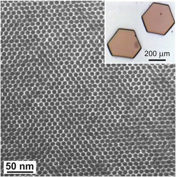
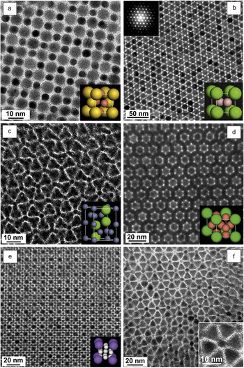
A beautiful thing about chemically synthesized nanostructures is their ability to form colloidal solutions. The colloidal stability is provided by surface ligands that introduce repulsion between individual NCs. Colloidal solutions of NCs can be used as an “ink” to print films of short-range ordered NCs or to build unprecedented structures where NCs pack into long-range ordered arrays, also known as “superlattices.”Reference Murray, Kagan and Bawendi6 The formation of superlattices occurs via self-assembly and is guided by entropy and weak interparticle forces. The simplest approach to grow such structures is to slowly evaporate the solvent, and if all particles are initially the same size, it is very likely to observe the formation of close-packed superlattices, such as the one shown in Figure 3.Reference Rogach, Talapin, Shevchenko, Kornowski, Haase and Weller19 This general phenomenon has been observed in many systems at various conditions. It is also possible to form more complex structures integrating several components, often with different and sometimes orthogonal properties. In a typical example, NCs with semiconducting (e.g., CdSe or PbS) and plasmonic (e.g., Au or Ag) properties can be synthesized separately and combined in one solution, followed by controlled evaporation of the carrier solvent. It was not difficult to find conditions that led to the formation of binary nanocrystal superlattices (BNSLs), which combine both types of NCs (Figure 4).Reference Shevchenko, Talapin, Kotov, O’Brien and Murray20, Reference Shevchenko, Talapin, Murray and O’Brien21 To determine the symmetry of three-dimensional NC packing, BNSL structures are typically inspected with a transmission electron microscope from different anglesReference Chen, Ye and Murray22, Reference Friedrich, Gommes, Overgaag, Meeldijk, Evers, Nijs, Boneschanscher, de Jongh, Verkleij, de Jong, van Blaaderen and Vanmaekelbergh23 or reconstructed from small-angle x-ray scattering data.Reference Smith, Goodfellow, Smilgies and Korgel24 It is common to find BNSLs isostructural with known salts or intermetallic compounds.Reference Shevchenko, Talapin, Kotov, O’Brien and Murray20 For example, the BNSL shown in Figure 4a is isostructural with a CuAu intermetallic compound, but instead of gold and copper atoms, it is built of approximately 8,000-atom-large modules of PbSe semiconductor and approximately 4,000-atom-large modules of Au metal. This is a powerful approach—we can use different building blocks, and we can assemble them into BNSLs with different structures and stoichiometries. Self-assembly of NCs is a general phenomenon, but it is not fully understood why and how these structures form. What is that magic process that brings NCs together and packs them into complex binary structures from a totally disordered initial colloidal solution?
Transmission electron microscopy image of a superlattice self-assembled from 7.5 nm PbS nanocrystals. The inset shows optical micrographs of three-dimensional “supercrystals” grown from nanocrystals.Reference Rogach, Talapin, Shevchenko, Kornowski, Haase and Weller19

Electron microscopy images of binary nanoparticle superlattices (BNSLs) self-assembled from various semiconductor, metallic, and magnetic nanocrystals. The bottom-right corner insets show the unit cells of corresponding structures. (a) AuCu-type BNSL formed by 7.6 nm PbSe and 5.0 nm Au nanocrystals; (b) AlB2-type BNSL assembled from 13.4 nm Fe2O3 and 5.8 nm PbSe nanocrystals. The top-left corner inset shows the small-angle electron diffraction pattern. (c) Laves phase MgZn2 type BNSL formed by 6.2 nm PbSe and 3.0 nm Pd nanocrystals. (d) CaCu5 type BNSL formed by 8.7 nm CdSe and 5.5 nm Au nanoparticles. (e) NaZn13 type BNSL formed by 5.8 nm PbSe and 3.0 nm Pd nanocrystals. (f) BNSL self-assembled from LaF3 triangular nanoplates (9.0 nm side) and 5.0 nm spherical Au nanocrystals. Adapted from Reference Reference Shevchenko, Talapin, Kotov, O’Brien and Murray20.

To address this question, we examined the thermodynamics of self-assembly. The change in free energy during formation of a NC superlattice generally follows the familiar expression:

where F is the Helmholtz free energy, U is the internal energy, and S is the entropy of the system. The first term (ΔU) is determined by the interactions between individual NCs through van der Waals, sterical, electrostatic, and other forces, whereas ΔS represents a global energy minimization rule that has its origin in a phenomenon known as “entropy-driven crystallization.”Reference Eldridge, Madden and Frenkel25, Reference Leunissen, Christova, Hynninen, Royall, Campbell, Imhof, Dijkstra, van Roij and van Blaaderen26 The general trend is that the entropic term favors the formation of the densest packing for a given combination of NCs. It favors BNSL formation if the packing density of a binary superlattice is comparable or exceeds the density of large and small NCs packed separately. If we deal with spherical particles, the diameter ratio (small to large spherical NCs) will be the parameter determining the type of binary lattice with the highest packing density. Based on rigorous free-energy calculations, the entropy alone can stabilize several binary lattices of spherical particles, including the very complex NaZn13 lattice (Figure 4e).Reference Eldridge, Madden and Frenkel25 The addition of interparticle forces can further stabilize low-density structures with efficient interactions between NCs. Which term in Equation 1 is more important? Our studies have shown that both terms provide comparable contributions to the total change in free energy.Reference Bodnarchuk, Kovalenko, Heiss and Talapin27 Moreover, temperature can be used to adjust the relative weights of the enthalpic and entropic terms in Equation 1 and to explore different regions of the phase diagram. Typically, at high temperatures when entropy dominates the game, we observed formation of BNSLs with highest packing density, whereas at low temperatures, less dense BNSL structures were observed whose formation could be rationalized as the interplay of the local van der Waals coupling between NCs in the unit cell and global energy minimization coming from the packing density in the lattice.Reference Bodnarchuk, Kovalenko, Heiss and Talapin27 On the practical side, temperature could be used to guide self-assembly of NCs toward desired BNSL structures.
Many key features of ordinary crystals, such as faceting, twinning, polymorphism, and defects, have been observed in NC superlattices,Reference Shevchenko, Talapin, Murray and O’Brien21, Reference Bodnarchuk, Li, Fok, Nachtergaele, Ismagilov and Talapin28 suggesting that their assembly follows the same fundamental principles as crystallization of conventional atomic and molecular solids. Compared to traditional atomic and molecular solids, BNSLs allow observing many complex lattices in real space, easily resolving individual NCs and revealing all structural details and defects. This class of materials provides a powerful tool for fundamental studies of solids, their structural defects and interfaces. As an example, self-assembled NCs helped us to solve several fundamental puzzles related to one of the most elusive and counterintuitive kind of solids—quasicrystals.
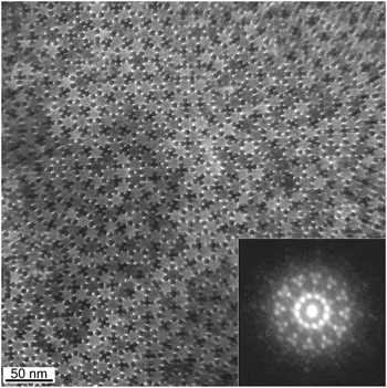
Quasicrystals are long-range ordered phases that lack translational symmetry and show symmetry operations forbidden in classical crystallography (e.g., five-, eight-, 10-, and 12-fold rotation).Reference Abe, Yan and Pennycook29 One of these “impossible” structures with 12-fold symmetry is shown in Figure 5.Reference Talapin, Shevchenko, Bodnarchuk, Ye, Chen and Murray30 This BNSL structure does not contain any periodically repeating elements but shows sharp electron diffraction peaks with 12-fold rotational symmetry. Another amazing thing about this BNSL is its irrational stoichiometry with  small NCs per each large NC. Such a structure has never been observed experimentally or anticipated by theoretical studies. However, these quasicrystalline structures spontaneously self-assembled from colloidal solutions containing different combinations of NCs (Fe2O3 and Au; PbS and Pd), all with the same NC size ratio of 0.43, showing that the size ratio rather than chemical nature of NCs was the key to obtain aperiodic quasicrystalline lattice. The BNSL structure shown in Figure 5 has higher packing density than any previously predicted binary sphere packing with quasicrystalline symmetry. The formation of such a dense structure was explained as an entropy-driven process based upon the efficient packing of spheres into an empty space, which was overlooked in previous studies of quasiperiodic structures.
A dodecagonal quasicrystalline superlattice self-assembled from 13.4 nm Fe2O3 and 5 nm Au nanocrystals. Inset shows a selected area electron diffraction pattern with crystallographically forbidden 12-fold rotational symmetry. Adapted from Reference Reference Talapin, Shevchenko, Bodnarchuk, Ye, Chen and Murray30.

Electronic coupling and charge transport in nanocrystal solids
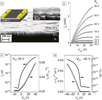
As we have seen, it is possible to build precisely engineered nanoscale building blocks and to make complex three-dimensional assemblies of these building blocks. The next natural step would be to use this approach for designing practical materials. However, to transform NC assemblies into competitive functional materials, one has to address an important fundamental problem of electronic communication between individual NCs. This is a very general problem, since the performance of NC-based devices is directly related to the efficiency of charge carrier injection (e.g., in LEDs) or extraction (e.g., in solar cells) to/from individual NCs.Reference Talapin, Lee, Kovalenko and Shevchenko31 In a NC array, the interfaces between NCs turned out to be the weakest links for charge carriers.Reference Vanmaekelbergh and Liljeroth32 The surface ligands with long hydrocarbon tails (e.g., oleic acid or hexadecylamine), which provide stability to the colloidal solution, also create insulating barriers around each NC. As a result, to move from NC to NC, electrons and holes have to hop or tunnel through these barriers.Reference Yu, Wang and Guyot-Sionnest33 The weak electronic coupling, combined with high Coulomb charging energy, typically leads to very poor electron mobility in NC assemblies.Reference Leatherdale, Kagan, Morgan, Empedocles, Kastner and Bawendi34 This is largely a chemistry problem. We need to learn how to modify the interfaces between NCs to make the pathways for electrons and holes as smooth as possible. In 2005, we reported a simple but amazingly efficient solution to this problem, by replacing original organic ligands with small-molecule hydrazine (N2H4).Reference Talapin and Murray35 Simply soaking the film of PbSe NCs in a dilute solution of N2H4 in acetonitrile displaced bulky insulating ligands (oleic acid) by N2H4, which brought the NCs closer together and increased conductivity by about 11 orders of magnitude.Reference Talapin and Murray35 That was how we made the very first field-effect transistor (FET) with a channel assembled of semiconductor NCs (Figure 6a). Those FETs could switch on and off by applying a gate voltage (Figure 6b), and the carrier mobility was about 1 cm2/Vs, very competitive to solution-processed organic semiconductors. In addition to improved electronic coupling, hydrazine behaved as a charge-transfer n-type dopant, providing mobile charge carriers to NCs.Reference Talapin and Murray35, Reference Norris, Efros and Erwin36 The conductivity of a PbSe nanocrystal solid can be switched from n-type to ambipolar and, finally, to p-type by simply controlling the number of hydrazine molecules adhered to the NC surface.Reference Talapin and Murray35
First nanocrystal-based transistors. (a) High-resolution cross-section scanning electron microscopy image of a field-effect transistor (FET) channel assembled from PbSe nanocrystals (NCs). The inset shows a schematic of a NC FET with source (S), drain (D), and gate (G) electrodes. (b–d) Typical output and transfer characteristics of n- and p-type PbSe NC FETs. (b) Plot of drain current I D versus drain-source voltage V DS, as a function of gate voltage V G for an FET with a channel composed of 8 nm PbSe NCs. (c) Plots of I D and I DS1/2 versus V G at constant V DS = 40 V used to calculate current modulation and field-effect mobility in the saturation regime for n-channel FET assembled from 8.1 nm PbSe NCs n-doped with hydrazine. (d) Plot of I D and I D1/2 versus V G at constant V DS = –40 V for p-channel FET assembled from 8.4 nm PbSe NCs. Adapted from Reference Reference Talapin and Murray35.

The improvements in the electronic coupling between NCs can be combined with engineering the structure of individual NCs. Instead of a simple metal or semiconductor, each NC can represent a multifunctional nano-heterostructure. For example, the arrays of “magnet-in-the-semiconductor” nanostructures (Figure 2f) showed semiconductor-type transport properties with magnetoresistance typical for magnetic tunnel junctions, thus combining the advantages of both functional components.Reference Lee, Bodnarchuk, Shevchenko and Talapin17 Field-effect devices with channels assembled from arrays of Au-PbS core-shell nanostructures demonstrated strong p-type doping that we attributed to the formation of an intra-particle charge transfer complex,Reference Lee, Shevchenko and Talapin18 similar to the charge transfer complex formed in a tetrathiafulvalene-tetracyanoquinodimethane (TTF-TCNQ) system.Reference Anderson, Lee and Saitoh37 These are the first examples of multifunctional materials assembled of electronically coupled nano-heterostructures. The field will move further toward more sophisticated and rationally engineered multifunctional building blocks. Compared to traditional molecular electronics that use organic molecules built of carbon, hydrogen, oxygen, and few other light elements, inorganic nanostructures can employ the entire periodic table to obtain building blocks with the desired bandgap, carrier effective mass, dielectric constant, magnetic moment, coercivity and other parameters. Inorganic semiconductors can cover a very broad range of bandgaps, from deep UV to mid-IR. However, one should always remember that the electronic properties of NC-based devices will be primarily determined by the transparency of the interfaces between individual nanostructures. Initially, we used hydrazine to replace bulky organic ligands, and numerous later studies explored different organic linkers for NCs, including aromatic and aliphatic dithiols (1,4-benzenedithiol, 1,2-ethanedithiol) and ethylenediamine.Reference Ethan, Harnik, Sean, Dean, Larissa and Edward38, Reference Liu, Gibbs, Puthussery, Gaik, Ihly, Hillhouse and Law39 One problem revealed in those studies was that, although small molecules really improved electrical conductivity, they were generally volatile and susceptible to oxidation. As a result, obtained conductive NC solids worked very nicely in a nitrogen-filled glovebox or in a cryostat, but would probably not survive for years in practical solar cells. With that kind of chemistry, everything we gained on the conductivity side came at the expense of long-term stability.
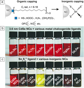
For a while, this seemed like a trap, but then we worked out ideas for designing NC interfaces in a way that was very different from everything tried before. Instead of using small organic linkers, we developed fully inorganic surface ligands for colloidal nanomaterials. As a first example, we found “metal chalcogenide complexes” (MCCs), shown in Figure 7, which are a rich family of molecular species combining only metals and chalcogens.Reference Kovalenko, Scheele and Talapin40, Reference Kovalenko, Bodnarchuk, Zaumseil, Lee and Talapin41 Typical examples of these new surface ligands include SnS44–, Sn2Se64–, In2Se42–, Ge4S104–, and AsS33–. We found that these ions have a very high affinity to surfaces of different NCs and nanowires. Typically, we synthesized nanomaterials following conventional protocols and then completely displaced organic ligands with MCCs, as shown in Figure 7a. Figure 7b shows colloidal solutions of CdSe nanoparticles capped with different MCC ligands. Each of these ligands can be applied to nanomaterials with different compositions and morphologies (Figure 7c), so this is a general chemistry.
(a) Schematic of the ligand exchange process used for preparation of all-inorganic nanocrystals (NCs) capped with SnS44– metal chalcogenide complex (MCC). (b) Stable colloidal solutions of 3.6 nm CdSe nanocrystals capped with various MCCs. (c) From left to right: stable colloidal solutions obtained by combining (N2H5)4Sn2S6 with 3.6 and 5.8 nm CdSe NCs, 9 nm CdTe NCs, 5 × 60 nm CdS nanorods (Nrods), CdSe nanowires (Nwires), 6 × 25 nm Bi2S3 nanorods, 5 nm Au NCs, and 3 nm Pd NCs. Adapted from References Reference Kovalenko, Scheele and Talapin40 and Reference Kovalenko, Bodnarchuk, Zaumseil, Lee and Talapin41.

The nanostructures with attached MCC ligands can be used as all-inorganic building blocks that form stable colloidal solutions in polar solvents such as dimethlysulfoxide, dimethylformamide, formamide, water, and hydrazine and preserve the electronic structure and photophysics of original quantum-confined semiconductors. These colloidal solutions can be used to form NC layers by printing or spin-coating. In such a close-packed NC film, the MCC ligands do not block electronic transport, thus linking individual nano-building blocks into an all-inorganic macroscopic assembly of strongly electronically coupled functional modules. We still have the quantum-dot-like electronic structure with excitonic features in the absorption spectrum. At the same time, strong coupling between the NCs allows for high electron mobility, up to 15 cm2/Vs in the films of 4 nm CdSe NCs capped with In2Se42– MCC ligands.Reference Lee, Kovalenko, Huang, Chung and Talapin42 This mobility is about an order of magnitude higher than that in the best solution-processed organic semiconductors. Moreover, near room temperature, these all-inorganic NC assemblies show a negative temperature coefficient of mobility, suggesting the band-like charge transport instead of previously observed hopping between localized sites.
We expect that the inorganic ligation of a NC surface will be widely used in future NC devices. This concept can go far beyond the MCC family. For example, we recently worked out chemistry for metal-free inorganic ligands, such as chalcogenides and hydrochalcogenides (S2–, HS-, Se2–, HSe–, Te2–, and HTe–), mixed chalcogenides (TeS32–), as well as OH– and NH2–.Reference Nag, Kovalenko, Lee, Liu, Spokoyny and Talapin43 These inorganic ions bind to the surface of semiconductor NCs and provide electrostatic stabilization for colloidal dispersions in polar solvents. These ligands are probably the simplest, cheapest, and smallest ones for colloidal NCs, and they can find broad use in NC-based devices. Very important, these inorganic ligands keep the chemistry simple and clean (What could be cleaner than stabilization of a CdSe NC surface with Se2– ions?), while providing efficient electronic coupling between individual NCs. Along similar lines, Kagan et al. reported remarkable carrier mobility in NC solids using SCN– surface ligands.Reference Fafarman, Koh, Diroll, Kim, Ko, Oh, Ye, Doan-Nguyen, Crump, Reifsnyder, Murray and Kagan44
Our next target is to generate NC assemblies combining all-inorganic design and strong electronic coupling with long-range order and regimentation between individual building blocks. This is still a work in progress. Quaternary ammonium cations are now used that allow tuning the interactions between MCC-capped NCs in a way favorable for self-assembly of single-component superlattices and BNSLs.Reference Kovalenko, Bodnarchuk and Talapin45 The latter case is especially exciting, since the formation of collective electronic states in BNSLs made of semiconductor-metal and semiconductor-magnet pairs will lead to unprecedented materials.
From fundamental to practical—Applications of nanocrystal solids
To bring NC-based materials into the arena of practical applications, one first has to identify the areas where these new materials can make lasting impact and successfully compete with existing technologies. At this time, the most feasible direction is to use NC colloids as a new form of solution-processed semiconductors.Reference Talapin, Lee, Kovalenko and Shevchenko31 If we were able to make an ink for printing semiconducting films with a carrier mobility comparable to that of traditional inorganic semiconductors, that would enable high-throughput (e.g., roll-to-roll) fabrication of large-area photovoltaics, LEDs, thermoelectrics, photodetectors, and printable electronics. Many theoretical and proof-of-principle studies have also emphasized the benefits of quantum-confined semiconductors for practical applications.
During the past several years, we explored different approaches to design practical materials from inorganic colloidal NCs. Thus, we demonstrated printable field-effect transistors using II–VI and III–V NCs capped with MCC and metal-free inorganic ligands.Reference Lee, Kovalenko, Huang, Chung and Talapin42, Reference Nag, Kovalenko, Lee, Liu, Spokoyny and Talapin43 These devices showed record electron mobilities for solution-processed semiconductors (Figure 8a); we also employed MCC-capped nano-heterostructures as sensitive photodetectors (Figure 8b).Reference Lee, Kovalenko, Huang, Chung and Talapin42 In these examples, MCC and metal-free inorganic ligands behave as electronically transparent “glue” for NCs. However, they can also be used for creating composite materials where the properties of NC and MCC components complement each other. It was first shown by Mitzi et al. that thermal decomposition of the hydrazinium-based MCCs, such as (N2H5)4Sn2S6 and (N2H5)2(N2H4)2In2Se4, can generate various chalcogenide phases (SnS2 and In2Se3 in the previous examples).Reference Mitzi, Kosbar, Murray, Copel and Afzali46, Reference Mitzi, Copel and Chey47 Combining electron-conducting nanostructures (e.g., CdS nanorods) with hole-conducting hosts (e.g., ZnTe or CuIn1–xGaxSe2) results in materials with a distributed network of p-n junctions. It is also possible to create new phases through solid-state reactions between NC and MCC ligands. As an example, we fabricated thermoelectric Bi2–xSbxTe3 nanostructured alloys using Bi2S3 nanorods and PbTe NCs with Sb2Te74– MCC ligands (Figure 8c).Reference Kovalenko, Spokoyny, Lee, Scheele, Weber, Perera, Landry and Talapin48 Upon gentle heating, this MCC decomposed into Sb2Te3–, releasing free tellurium that immediately reacted with the Bi2S3 phase (Bi2S3 + 3Te → Bi2Te3 + 3S), leading to the formation of the nanocrystalline p-type Bi2–xSbxTe3 composite phase. P-type (Bi, Sb)2Te3 and n-type (Bi, Sb)2(Te0.9Se0.1)3 exhibited high Seebeck coefficients of ±200–250 μV/K and conductivities up to 450 S cm–1, closely approaching values required for commercial applications. High power factors 20.4 μW cm–1 K–2 and dimensionless thermoelectric figure of merit (ZT) values of 0.7 were obtained.Reference Kovalenko, Spokoyny, Lee, Scheele, Weber, Perera, Landry and Talapin48
Colloidal nanocrystals as soluble precursors for inorganic semiconductors. (a) High electron mobility in a spin-coated layer of 3.9 nm CdSe nanocrystals bridged with In2Se42– molecular metal chalcogenide ligands. The mobility decreased with increasing temperature, typical for the band-like charge transport. (b) Photoconductive response at 500 nm measured for an array of CdSe/CdS core-shell nanocrystals bridged with In2Se42– ligands. The combination of highly mobile electrons distributed between CdSe cores and CdS shells and the holes strongly confined to the CdSe cores provide high internal photoconductive gain in the CdSe/CdS nanocrystal solids.Reference Lee, Kovalenko, Huang, Chung and Talapin42 (c) Transmission electron microscopy image of a thermoelectric PbTe/(Bi,Sb)2Te3 nanostructured composite prepared by combining PbTe and Bi2S3 nanocrystals, both capped with Sb2Te74– molecular metal chalcogenide complex.Reference Kovalenko, Spokoyny, Lee, Scheele, Weber, Perera, Landry and Talapin48 This approach allows for the preservation of the benefits of nanostructuring and quantum confinement while enabling facile charge transport through the interparticle boundaries necessary for high thermoelectric efficiency. The insets show corresponding colloidal solutions used as precursors for the deposition of functional materials. Adapted from References Reference Lee, Kovalenko, Huang, Chung and Talapin42 and Reference Kovalenko, Spokoyny, Lee, Scheele, Weber, Perera, Landry and Talapin48.

Conclusions and outlook
Building functional materials through “modular” assembly of electronically coupled nanoscale units requires creative approaches to the synthesis of individual nanostructures, packing them into desired superstructures, and coupling them electronically. This approach allows breaking synthesis of functional solids into several independent steps. This mimics step-by-step syntheses typical for molecular chemistry but very uncommon in solid-state chemistry, where all transformations typically occur in one pot. We can precisely engineer individual building blocks, and we can pack these “bricks” into different superlattices by using guided self-assembly. Nanocrystal (NC) superlattices provide a convenient test bed for fundamental studies of crystallization phenomena. We can also use these systems to address very fundamental questions related to optimal packing of objects with complex shapes and formation of structural defects and interfaces. The ability to assemble precisely engineered nano-building blocks into multicomponent assemblies is opening the door to a new generation of functional materials where components and functionalities can be added, tuned, or combined in a predictable manner.
Development of surface chemistry for efficient electronic coupling of individual nano-building blocks represents an equally important problem, critical for the success of NC-based materials. The role of surface chemistry is to electronically passivate the NC surface without blocking charge transport between NCs or from NCs to surrounding matrix. Significant research efforts in this area are driven by the hope to employ NC solids in solar cells, LEDs, and thermoelectric devices. It is also very likely to observe emergence of new phenomena in multicomponent NCs assemblies where individual NCs couple to form collective electronic states.Reference Urban, Talapin, Shevchenko, Kagan and Murray49 These new materials built of strongly coupled NCs will be a source of rich new physics and chemistry and will find multiple technological applications.
Acknowledgments
I want to express my greatest respect to my wonderful group of postdocs, students, and collaborators—I am very proud to be a part of this team. I would also like to use this opportunity and thank those who introduced me to different facets of nanomaterials, especially Horst Weller, Chris Murray, and Paul Alivisatos. Many thanks to the funding agencies for supporting this work, in particular, NSF CAREER under Award Number DMR-0847535, the Office of Naval Research under Award Number N00014–10–1-0190, and the David and Lucile Packard Foundation. Finally, I am very thankful to MRS for selecting me for the Outstanding Young Investigator Award, especially when I think of those who have received it in the past.

Dmitri Talapin is an associate professor in the Department of Chemistry and James Frank Institute at the University of Chicago. He received his doctorate degree from the University of Hamburg, Germany, in 2002 under the supervision of Horst Weller. In 2003, Talapin joined the IBM Research Division at T.J. Watson Research Center as a postdoctoral fellow to work with Chris Murray on the synthesis and self-assembly of semiconductor nanostructures. In 2005, he moved to Lawrence Berkeley National Laboratory as a staff scientist at the Molecular Foundry. He joined the faculty at the University of Chicago in 2007. His recent recognitions include the Camille Dreyfus Teacher Scholar Award; David and Lucile Packard Fellowship in Science and Engineering; NSF CAREER Award; and Alfred P. Sloan Research Fellowship. He serves on the advisory board of Nanoscale, which is published by the Royal Chemical Society. Talapin can be reached by email at dvtalapin@uchicago.edu.