I. INTRODUCTION
The market of future tunable telecommunication systems strongly demands for tunable filters for an equally diverse pool of communication, radar, electronic warfare, and sensing systems. These filters will enable new system architectures, which will allow for improved performance and new capabilities. Despite a strong demand for such filters, it is not easy to identify a technology that satisfies all requirements, such as high Q, high selectivity, low power consumption, small form factor, fast tuning speed, etc [Reference Peroulis, Naglich, Sinani and Hickle1].
Different technologies have been investigated so far [Reference Uher and Hoefer2, Reference Courreges, Li, Zhao, Choi, Hunt and Papapolymerou3], but an acceptable trade-off among wide tuning range, high Q, low cost, and small size has not been fully achieved. RF MEMS is one of the most attractive solutions for microwave applications thanks to its low loss, low power consumption, low cost and compact size [Reference Park, Reines, Patel and Rebeiz4, Reference Winter and Mansour5]. High-Q tunable filters appear therefore to be obtainable by suit ably combining RF-MEMS and high-Q cavity resonators. In [Reference Stefanini, Chatras, Pothier, Orlianges and Blondy6] a MEMS varactor located at the electric field maximum has been used in a ridged cavity at 5 GHz to tune its resonant frequency. The measured Q is above 500 for a tuning range of 500 MHz.
Similar results have been obtained for a 13 GHz surface-mounted cavity [Reference Stefanini, Martinez, Chatras, Porthier, Boria and Blondy7]. However, to obtain high Q in a MEMS tunable waveguide filter, not only the MEMS switch should show very low contact resistance, but also its integration in the cavities should be carefully designed and modeled. In [Reference Pelliccia, Bastioli, Casini and Sorrentino8, Reference Pelliccia, Cacciamani, Farinelli, Ligander, Persson and Sorrentino9] an interesting tuning principle has been proposed, but it requires several MEMS switches per cavity. The biasing network as well as the MEMS substrates should be taken into account, since they could significantly degrade the filter performance and vanish the advantage of using MEMS. Most often, this translates the need for custom design of RF MEMS switches that have to be adapted to the specific filtering structure and operating frequency.
This paper presents the design, manufacturing, and measurement of an innovative waveguide adjustable filter based on commercially available MEMS switch. The integration of the MEMS components into TE101 mode cavities has been modeled by using full-wave simulator and a second-order filter in K-band has been realized as a first proof of concept. Particular attention has been devoted to the minimization of the number of tuning elements per cavity so as to reduce the filter complexity, cost, and loss due to the biasing circuitry. The case of a waveguide filter for terrestrial radio-link telecommunications (i.e. mobile back-hauling) at K-band has been considered.
II. FILTERS FOR MOBILE BACK-HAULING SYSTEMS
Microwave and millimeter-wave communication systems are rapidly broadening due to the advantages offered over ordinary wireless links. They grant the use of wideband radio links useful for inter-satellite and personal communications. Commercially available systems are constantly under development and subject to continuous improvements at frequency ranges from 4 to 80 GHz. Commercial systems need high yield and the possibility to produce huge numbers of devices by means of low cost manufacturing processes. One of the major limiting components of microwave and millimeter-wave communication systems are the transmit/receive filters. This technology is usually implemented in waveguide in order to provide low insertion loss and high channel-to-channel isolation. The drawbacks related to such a technology are typically due to manufacturing cost and size.
Moreover, the passbands imposed by the guidelines for frequency channel allocation for fixed wireless systems (ECC Recommendations) are typically too wide and the guard bands used to separate the transmission and receiving channel are usually very narrow. Consequently, a single mobile back-hauling system is unable to cover the whole bandwidth, requiring the use of multiple radio system, covering just one part of the bandwidth. As a consequence, the transmission/receiving filters will be tuned on a single portion of the frequency range, in order to avoid the use of high-order filters, which would drastically increase their size and mass and would definitely complicate the design workflow.
The goal of the solution shown in this paper is to overpass the drawback described, by means of a single high-Q filter in K-band, capable of covering the whole spectrum established by the recommendations. If the operating frequencies of back-hauling systems are in the range 18–42 GHz, the expected number of frequency states in the K-band can be three at most, while the tuning range can be typically up to 5–10%, but even smaller. As a preliminary case study we considered here a sub-band of the K-band frequencies that requires a smaller tuning range (1%) and only two frequency states.
III. THE TUNING CONCEPT
The simplest way to trim the resonant frequency of a cavity is to perturb the electromagnetic field of the resonant mode. The perturbation can be applied to either the EM field or to the current flowing on the inner metal wall of the cavity. In the latter case, the current distribution can be varied by introducing one or more switches located in the region of the maximum current magnitude, as explained below.
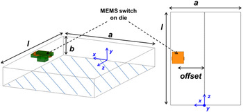
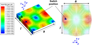
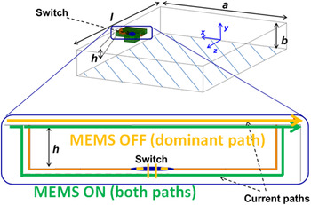
In Fig. 1, the MEMS-based tuning principle proposed here is applied to a rectangular cavity of length l, width a, and height b, operating at TE101 mode. The MEMS switch is located in a region of maximum current amplitude, i.e. in the center of the length l, as shown in Fig. 2. The switch, connected to the cavity broad wall by ribbon-bonding, is placed above a dielectric substrate of thickness h and oriented along the current direction, so as to create, when in the on-state, an additional current path, as shown in Fig. 3. When in the off-state, instead, a dominant path is present. In this configuration, the current distribution of the TE101 mode is perturbed depending on the switch state, obtaining two different resonant frequencies. The larger the ratio h/b between the substrate thickness and the waveguide height, the larger is the distance between the two frequencies.
Two views of the 3D model of the proposed tunable cavity using MEMS switch on die.

Current distributions in HFSS of a TE101 mode and selected position of the switch in the cavity.

Current paths in the proposed tunable cavity.

The ohmic cantilever MEMS switch used here consists of a thin gold membrane suspended above an interrupted signal line and anchored at one end. The membrane is electrostatically actuated by applying a voltage (~70–90 V) to an electrode (actuation pad) located below the membrane. The switch can be modeled as a small series resistance when in the on-state, and as a series capacitance of a few fF in the off-state [Reference Courreges, Li, Zhao, Choi, Hunt and Papapolymerou3, Reference Stefanini, Chatras, Pothier, Orlianges and Blondy6].
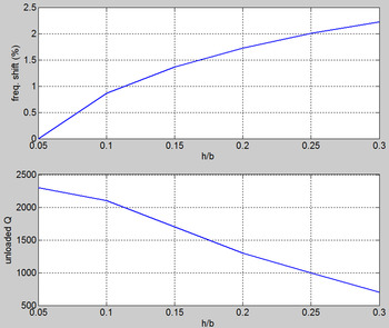
The amount of frequency shift to adjust the filter response can be controlled by changing the ratio h/b and the position of the MEMS on the broad wall with respect to maximum current. Q factors up to 1000 can be obtained at K-band (using standard WR-42 width having a height of 1.5 mm) with tuning range of 2% using low-loss substrate. See Fig. 4 where behavior of frequency shift and unloaded Q is shown when h/b is increased. These results are calculated in HFSS at 23 GHz when MEMS quartz substrate thickness is fixed at 0.350 mm. As a matter of principle, intermediate frequency shifts can be achieved by using more MEMS switches and activating only some of them separately.
Frequency shift (%) and unloaded Q when h/b is increased. These results are calculated in HFSS at 23 GHz when MEMS quartz substrate thickness is fixed at 0.350 mm.

IV. DESIGN OF K-BAND MEMS TUNABLE FILTER
Thanks to the performances of the existing commercially available mathematical tools, the design of waveguide filters exhibits today a straightforward procedure. The filter has been synthesized from the ideal Chebychev response of its state OFF, translated to waveguide components (cavities, irises/posts and MEMS switches size and position) and optimized to meet the requirements in the filter passband. Local optimization techniques (Nelder–Mead or other simplex-based methods, [Reference Lagarias, Reeds, Wright and Wright10]) usually achieve acceptable results, as long as the behavior of the waveguide components resembles that of their lumped counterparts, i.e. the frequency range is not extremely wide with respect to the center frequency.
S 11 obj (f i ) denotes henceforth the goal value of the return loss at a frequency fi. S 11(f i , x) is the TE101 reflection coefficient of the structure to optimize as a function of a given set of geometrical dimensions, gathered in the vector x. f BP is here defined as the set of frequencies of the reflection zeros and of the reflection maxima in the passbands of the two filters. The cost function GF(x) is thus defined as
 $$GF({\bf x}) = {\sum\limits_{i \vert {f_i} \in {f_{{\bf BP}}}} {\left( { \vert {S_{11}}({f_i},{\bf x}) \vert - \vert {S^{obj}_{11}} ({f_i}) \vert} \right)} ^2}.$$
The outcome of this common optimization process is the ideal filter, which theoretically fulfills the given specifications. To compensate in advance for the effects of fabrication tolerances, approximate modeling and frequency switching due to the use of the RF MEMS, the ideal filter should be optimized to fulfill stricter requirements than the actual ones, as described in [Reference Cannone and Oldoni11]. Thus, the filter is optimized to meet stricter specifications than the required ones, in order to make the design more robust to modeling inaccuracies and fabrication tolerances described in Section V. A yield analysis is also carried out to estimate the effect of random variations of the physical dimensions. One of the problems regularly faced at this point is that the design may be extremely sensitive to such inaccuracies, mostly introduced by milling and galvanic treatment. This in turn requires demanding stricter fabrication tolerances, which usually worsens both the mechanical yield and manufacturing times.
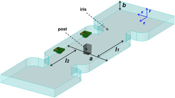
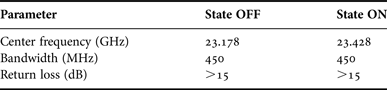
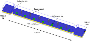
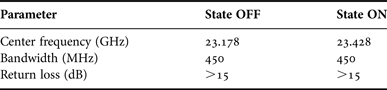
Figure 5 shows the HFSS model of a K-band second-order filter based on the proposed tuning concept, after the optimization process. The requirements are listed in Table 1.
HFSS design of the manufactured MEMS-based tunable second-order filter at K-band.

Filter requirements.
The filter structure consists of two TE101 mode cavities coupled by using a vertical post and connected to input/output waveguide sections by inductive irises. Each cavity is loaded with an ohmic MEMS switch that is bonded with a ribbon to a broad cavity wall. The MEMS switches are commercially available series ohmic switches realized on HR Silicon substrate and based on electrostatic actuation. The switches are provided with a HR Silicon 0-level hermetic cap so as to ensure inert operating environment. The MEMS membrane has been modeled in HFSS as 3 Ω series resistance (Ron) when in the on-state (cantilever down), and as a series capacitance (C off ) of 15 fF in the off-state (cantilever up). These values fit well with the RF measurements of the MEMS.
The two switches are activated simultaneously in order to modify the electromagnetic field and current distribution of the TE101 mode inside the cavities and, thus, shift the resonant frequencies.
Different tuning ranges can be obtained by varying the position of the MEMS switches inside the cavities along the x-axis and by changing the cavity height b. In the case of a waveguide filter operating in K-band, the shift may range from a few tens of MHz up to some hundreds of MHz: the lower b, the larger the offset, the larger the frequency shift. On the other hand, also the Q-factor is affected by the tuning: the larger the tuning, the lower the Q, the higher the loss in the filter. As the cavity height b is reduced to achieve larger h/b ratios, thus larger frequency shifts (h is fixed by the MEMS technology), in fact, the quality factor is also reduced. Moreover, since also the filter couplings are modified by the switch activation, tuning ranges larger than 2–3% would require additional tuning elements for coupling compensation.
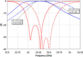
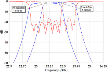
Figure 6 shows the narrowband and wideband simulated performance in terms of S-parameters of the second-order filter design in HFSS. When both switches are in off-state the filter is centred at 23.178 GHz, showing a 20 dB bandwidth of 1.45%. When the switches are activated, the filter response is shifted upwards and centered at 23.428 GHz (250 MHz shift), while preserving good performance in terms of return loss and bandwidth.
HFSS S-parameters of the MEMS-based tunable second-order filter at K-band in Fig. 5 (OFF state: solid lines. ON state: dashed lines).

V. MANUFACTURING
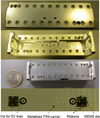
Figure 7 shows the manufactured second-order filter. The body consists of a silver-plated WR-42 waveguide (10.688 × 4.318 mm2). As explained in Section IV, in order to obtain the desired tuning range, we should change the cavity height b, in this case chosen equal to 1.5 mm. The production process necessarily originates inaccuracies on the geometry. The filter is done by milling a piece of prime material (typically aluminum or brass). Consequently, it is subject to a number of fabrication defects basically regarding the expected geometrical length and thickness of irises/posts and cavities. In this particular case, the filter has been manufactured with an accuracy of ±0.03 mm, in order to avoid high production costs.
Photographs of the manufactured MEMS-based tunable second-order filter at K-band.

Another aspect of interest is the thickness of the galvanic treatment layer. Typical values are shown in Table 2. The galvanic treatment may also be inhomogeneous and thus unpredictably affect the cavities and septa/posts shape.
Galvanic treatment layers.

Therefore, tuning screws are required in order to compensate the variation of the transfer function due to the manufacturing inaccuracies provided by the milling process.
The main lid of the filter consists of a silvered FR4 PCB whose height is equal to 1.524 mm (60 mils). The MEMS switches are glued into the milled cavity broad wall and electrically connected to the wall using ribbon bonding technology. The latter introduces parasitic inductances, which should be properly considered during the design phase. The MEMS biasing lines are driven to the external part of the filter by using vertical vias. The entire gluing and mounting process is developed inside a clean room. In fact, generally in the process of semiconductor manufacturing, the airborne particles permanently deteriorate the photo etched parts forming the chip, creating a flawed electronic circuit, and as a consequence a production scrap. Both airs coming from outside and inside the clean room are finely purified in order to remove dust, by means of dedicated air filters used to eliminate generated impurities.
In order to avoid leakage of microwave radiation due to a defective contact between the main body of the diplexer and the PCB lid, one should typically place the tightening screws in the immediate vicinity of the waveguides. To improve the accuracy of this contact, a narrow (0.5 mm) trench should be cut in the main body following the perimeter of the waveguide.
An additional lid made in silvered aluminum is finally placed above the main FR4 lid, in order to increase the pressure and to prevent signal loss due to an insufficient contact.
VI. EXPERIMENTAL RESULTS
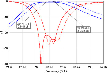
The measured |S21| parameters are shown in Fig. 8 for both MEMS states. The input RF-power is 0 dBm and the DC bias voltage of the switches is 90 V.
RF Measured S-parameters of the MEMS-based tunable second-order filter at K-band in Fig. 5–7 (OFF state: solid lines. ON state: dashed lines).

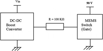
In order to preserve the integrity of the MEMS switch, due to the high DC bias voltages required, the voltage source must be provided by means of a DC–DC Converter Boost, as shown in Fig. 9. The DC–DC Converter must be properly designed in order to obtain an output voltage equal to the DC bias required for the considered MEMS Switch. Moreover, a 100 KΩ resistance is inserted between the DC–DC converter and the gate of the MEMS Switch, in order to protect this one from excessive current absorptions, preserving the component from damaging.
Voltage supply scheme of the MEMS.

The measured off-state resonant frequency is very close to the requirement. The measured frequency shift from on- to off- state is 160 MHz (~0.7%). Such value is smaller than the simulated one (250 MHz). This is to be mainly ascribed to the parasitics associated with the bonding ribbons being longer than the designed ones. The measured Qs are about 1000 in the on-state and 500 in the off-state. The larger insertion loss, mainly in the off-state is due to the higher tanδ of the HR silicon. The Q reduction in the off-state is due to the loss of the HR Silicon of the MEMS substrate and 0-level cap; it could be improved by adopting for the MEMS device a substrate with lower loss, such as Quartz. Additional loss may be due to radiation through the vias; this can be minimized by a proper miniaturization of the vias.
Graph in Fig. 10 shows the simulated S-parameters of a seventh-order filter design based on the same concept used for the second-order filter in Figs 5–8. The filter is designed in order to fulfill electrical requirements provided by SIAE Microelettronica for its next generation of tunable two-state filters in K-band apparatus. The required bandwidth of the seventh-order filter is 500 MHz with an Insertion Loss below 2 dB: this implies a minimum unloaded Q of the resonators below 1000. The frequency shift is 252 MHz and the insertion loss is below 2 dB in both frequency states with fractional bandwidth of 2%. The device will be fabricated using only seven MEMS switches on low-loss quartz substrate (i.e. only one switch per resonator).
S-parameters of the MEMS-based tunable seventh-order filter at K-band based on concept in Fig. 5 (OFF state: solid lines. ON state: dashed lines).

As shown in Fig. 4, higher tuning range can be achieved at the expense of the unloaded Q. If Qs are up to 1000, the maximum achievable tuning range should be in the order of 2%. If the tuning range is small, as in the case here presented, the filter bandwidth remains virtually unchanged in the different frequency states. If higher tuning ranges are desired, other types of coupling mechanisms of the filters are recommended. E-plane waveguide filters, for instance, allow for bandwidth that are more stable over frequency tuning, since these filters are based on coupling mechanisms that are more stable and constant in frequency (Fig. 11) [Reference Pelliccia, Cacciamani, Farinelli, Ligander, Persson and Sorrentino9].
HFSS-model of the MEMS-based tunable seventh-order filter at K-band based on concept in Fig. 5.

VII. CONCLUSIONS
The first experimental results of a novel MEMS-based waveguide filter for mobile back-hauling at K-band with adjustable center frequency have been presented. The filter employs commercial packaged RF MEMS switches. The switches are used to perturb the electromagnetic field of the TE101 mode so as to tune the resonant frequency of the cavity. Measurements show a 160 MHz frequency shift (0.7%) and Qs up to 1000 using only one MEMS Switch per resonator. New higher order prototypes using low-loss substrate MEMS (e.g. quartz) will be fabricated to increase the Qs.
The concept present here leads to a very simple structure. The number of MEMS per resonator is, in fact, minimized (we use only one MEMS) and the design is simple. On the other hand, the achievable tuning range is lower (<2%) than the other concepts. Higher tuning ranges are achievable using more MEMS, but at the expense of lower Qs of the resonators.
 Luca Pelliccia was born in Foligno, Italy, in 1984. He received the Laurea degree (with distinction) in Electronic Engineering from the University of Perugia, Perugia, Italy in April 2009. In 2008–2009, he carried out his thesis research with Ericsson AB, Mölndal, Sweden, on high-Q and compact waveguide filters and matching transitions and interconnections for microwave applications at high frequencies. In November 2012 he received his Ph.D. degree at University of Perugia with a thesis titled “Tunable and Miniaturized Waveguide Filters for Advanced Communication Systems” under the advice of Prof. Roberto Sorrentino. He is currently working at RF Microtech Srl (an associate member) as RF and microwave R&D engineer. His research and design activities include innovative and low-cost solutions for compact filters and diplexers and new concepts for tunable, reconfigurable and miniaturized waveguide bandpass filters.
 Paola Farinelli received the Laurea degree (with distinction) and the doctoral degree in Electronic Engineering from the University of Perugia, Italy, in 2002 and 2006, respectively. Her research activity focuses on the electromagnetic modeling and design of reconfigurable RF MEMS components and circuits. She is a cofounder and project manager at RF Microtech, born in 2007 as a spin-off company of the University of Perugia.
 Roberto Sorrentino is a Professor at the University of Perugia, Italy. His research activity deals with the analysis and design of microwave and millimeter-wave circuits and antennas. He is author or co-author of more than 150 technical papers in international journals, 300 refereed conference papers and three books and is a IEEE Fellow (1990), recipient of the MTT-S Meritorious Service Award (1994), the IEEE Third Millennium Medal (2000), Distinguished Educator Award from IEEE MTT-S (2004). He was the Editor-in-Chief of the IEEE Microwave and Guided Wave Letters (1995–1998) and was among the founders and President of the European Microwave Association (1998–2009).
 Giandomenico Cannone was born in Bari, Italy, in 1984. He received the M.Sc in Telecommunications Engineering at the Politecnico di Milano, Italy, in July 2009 with a thesis on the design of microwave diplexers for satellite applications with Universidad Politecnica de Madrid (ETSIT). He is currently working as Microwave Engineer at SIAE Microelettronica S.p.A and his activity is related to the development of waveguide diplexers, hybrid couplers, orthomode transducers and antennae measurement.
 Giulio Favre was born in Aosta, Italy, in 1967. He received the Laurea degree at “Politecnico di Torino” in 1993 with a thesis on DRO. He has worked in Siemens Telecommunications as a microwave designer, from 1998 to 2001. He has worked in Ericsson Telecommunications as a MMIC designer. Since 2002 he has been working in the Siae Microelettronica S.p.A. laboratory. Most of his activities are related to passive and active circuits design for microwave transceivers for Telecomm applications.
 Piero Coassini was born in Milano, Italy in 1960. He received the M.Sc. in Telecommunications Engineering at the Politecnico di Milano in 1986 with a thesis on lumped devices in matching network for microwave amplifier. He has worked in Telettra Telecommunication as responsible of microwave power amplifiers from 1985 to 1990. Since 1990 he has been working in R&D of Siae Microelettronica as Microwave Laboratories Director.