Introduction
The microwave power dividers (PDs) are among the key passive components and have been widely used in wireless communication circuits and phased antenna arrays [Reference Abbosh1, Reference Bo and Liu2]. PDs with an out-of-phase response are highly demanded in balanced circuit designs, such as push–pull amplifiers, multipliers, and balanced mixers [Reference Deal, Radisic, Qian and Itoh3, Reference Chiu, Yum, Xue and Chan4]. To achieve the out-of-phase features, several balanced transmission lines, such as double-sided parallel-strip lines [Reference Yang, Chen and Xue5], microstrip-slot lines [Reference Ogawa, Hirota and Aikawa6] have been investigated in recent years. However, the design procedure of out-of-phase PDs with favorable isolation performance using traditional microstrip lines still needs to be further explored.
In this paper, a PD with a shunt stub for isolation connected between the two output ports of a traditional Marchand balun is presented. In addition, the patterned ground-plane technique is applied to achieve the wideband performance [Reference Guo, Zhang and Ong7]. It can be integrated with other microwave components for broadband applications.
Analysis and design
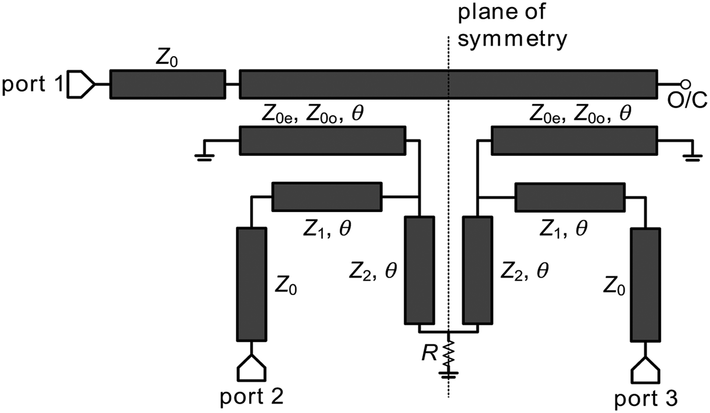
The proposed configuration of the divider is shown in Fig. 1. A shunt half-wavelength high impedance line with a shorted isolation resistor placed in the middle to realize the perfect matching at output ports and high isolation between them. Due to the symmetry of the proposed structure, it can be synthesized by using the even–odd-mode analysis method. The two-port circuit models of the wideband PD in Fig. 1 under even–odd-mode excitations are shown in Figs 2(a) and 2(b). By choosing θ to be π/2 at the center frequency, the corresponding input impedance is
 $$Z_{in,e1} = \displaystyle{{2{(Z_{0e}-Z_{0o})}^2(Z_{0e} + Z_{0o})} \over {8Z_0(Z_{0e} + Z_{0o}) + 16Z_{0e}Z_{0o} + (3Z_{0o}-Z_{0e}){(Z_{0e}-Z_{0o})}^2Z_p}}$$
 $$Z_{in,e2} = \displaystyle{{Z_{in,e1}Z_2^2} \over {Z_{in,e1}R + Z_2^2}} $$
Here, Z p is characterized as Z P = (Z 0e + Z 0o)/Z 0eZ 0o. Similarly, when the odd-mode excitation is applied, the corresponding input impedance of Z in,o1,Z in,o2 is
 $${Z_{in,o1}} = {Z_{in,o2}} = \displaystyle{{{2{Z_0}{Z_{0e}}{Z_{0o}}(3{Z_{0o}} - {Z_{0e}}) + 4Z_{oe}^2Z_{0o}^2}}\over{{16{Z_0}Z_q^2 + {Z_0}{{(3{Z_{0o}} - {Z_{0e}})}^2} + 2{Z_{0e}}{Z_{0o}}(3{Z_{0o}} - {Z_{0e}})}}}$$
where Z q is characterized as Z q = Z 0eZ 0o/(Z 0e − Z 0o). The relation Z in,e2 = Z in,o2 should be satisfied to achieve perfect impedance matching at output ports. The value of R can be found accordingly as
 $$R = \displaystyle{{Z_2^2 (Z_{in,e1}-Z_{in,o1})} \over {Z_{in,e1}Z_{in,o1}}}$$
Circuit model of the proposed out-of-phase PD.

Even- and odd-mode equivalent circuit of the wideband out-of-phase PD: (a) even mode and (b) odd mode.

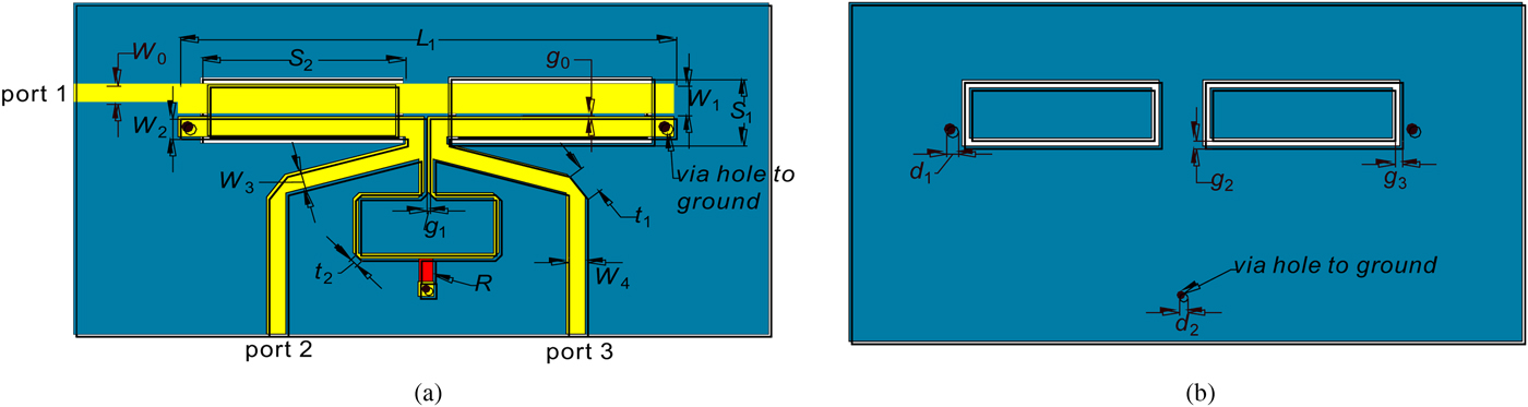
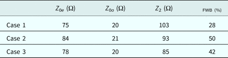
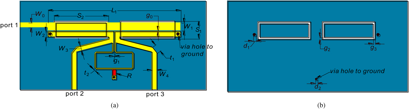
In order to maintain the in-band return loss higher than 20 dB, three filter cases with different fractional bandwidths (FBWs) of odd-mode equivalent circuit are presented, the design parameters of which are listed in Table 1. The FBW of the proposed PD can be adjusted accordingly by tuning the values of Z 0e, Z 0o, and Z 2. In this design, the parameters of case 2 are selected to obtain the desired bandwidth, and the value of R is calculated as 108.3 Ω according to (3). A defected ground structure (DGS) is applied to meet the needed even-/odd-mode value. The proposed planar Marchand balun wideband PD is shown in Figs 3(a) and 3(b).
Layout of the fabricated wideband out-of-phase PD: (a) top layer and (b) bottom layer.
Design parameters of three filter cases with different FBWs

Implementation and measurements
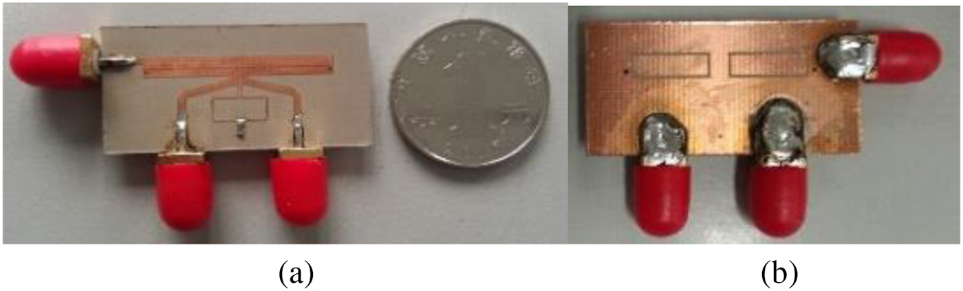
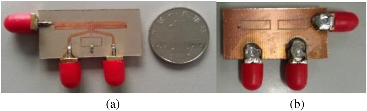
The frequency characteristic of the proposed PD was studied by the full-wave simulator ANSYS HFSS v.15, and one prototype divider was fabricated on a two-layer PCB, Taconic RF-35, with a dielectric constant of 3.5 and a thickness of 0.508 mm. Figures 4(a) and 4(b) show the photographs of the fabricated wideband PD with a circuit size of 28.6 × 13.23 mm2 (0.59 × 0.27 $\lambda _g^2 $). The theoretical parameters were optimized and the final dimensions are: W 0 = W 4 = 1.1 mm, W 1 = 1.8 mm, W 2 = 1.23 mm, L 1 = 28.56 mm, t 1 = 1.72 mm, t 2 = 0.5 mm, g 0 = 0.1 mm, g 1 = 0.2 mm, g 2 = 0.47 mm, g 3 = 0.44 mm, S 1 = 3.93 mm, S 2 = 11.71 mm, d 1 = 0.7 mm, d 2 = 0.5 mm, and R = 82 Ω.
Photograph of the proposed wideband PD: (a) top view and (b) bottom view.
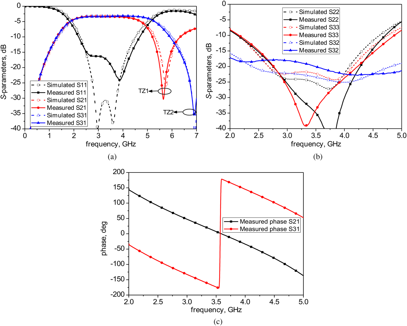
The simulated and measured results are provided in Figs 5(a)–5(c). The measured passband is centered at 3.43 GHz, with a 15 dB FBW of 53.86%. Since the input port is not completely symmetrical with respect to the overall circuit, the two transmission zeros are not at the same frequency point. Two transmission zeros (TZ1, TZ2) separately corresponded to S 21 and S 31 are located at 5.65 and 6.9 GHz. Equal power division (3.32 ± 0.22 dB) for simulated results is achieved in the passband, while the measured insertion losses are 0.52 ± 0.21 dB (not including the 3 dB division loss). The measured insertion loss is slightly higher than the simulation result due to the machining accuracy and the error introduced by the measurement. Figure 5(b) verifies the simulated isolation performance of more than 17 dB in the frequency range of 2.51–4.36 GHz. The increased output return losses compared with the simulated ones depict the higher performance in practical. Besides, Fig. 5(c) shows the measured phase, which indicates good out-of-phase performance. Table 2 shows the performance of this work compared with other work.
Simulated and measured results of the proposed wideband PD: (a) input return loss and insertion loss, (b) output return loss and isolation and (c) phase.
Comparison between this work and other studies

IL, insertion loss; Iso, isolation; RL, return loss.
Conclusion
A planar PD with wideband frequency response and favorable isolation performance has been presented. By applying an out-of-phase isolation technique to Marchand balun, the proposed PD exhibits higher performances for output impedance matching and isolation compared with the wideband out-of-phase PDs introduced in [Reference Yang, Chen and Xue5, Reference Ogawa, Hirota and Aikawa6], which can make it more suitable for practical use. For example, it is applied to circuits such as array antennas and power amplifiers.
Author ORCIDs
Fei Xia, 0000-0003-3654-8775
Acknowledgements
This work was supported by the National Natural Science Foundation of China under grant 61771094.
 Kaijun Song (M'09-SM'12) received his M.S. degree in radio physics and his Ph.D. degree in electromagnetic field and microwave technology from the University of Electronic Science and Technology of China (UESTC), Chengdu, China, in 2005 and 2007, respectively. Since 2007, he has been with the EHF Key Laboratory of Science, UESTC, where he is currently a full Professor. From 2007 to 2008, he was a postdoctoral research fellow with the Montana Tech of the University of Montana, Butte, USA, working on microwave/millimeter-wave circuits and microwave remote sensing technology. From 2008 to 2010, he was a research fellow with the State Key Laboratory of Millimeter Waves of China, Department of Electronic Engineering, City University of Hong Kong, on microwave/millimeter-wave power-combining technology and Ultra-Wideband (UWB) circuits. He was a senior visiting scholar with the State Key Laboratory of Millimeter Waves of China, Department of Electronic Engineering, City University of Hong Kong in November 2012. He has published more than 180 internationally refereed journal papers. His current research fields include microwave and millimeter-wave/THz power-combining technology; UWB circuits and technologies; microwave/millimeter-wave devices, circuits and systems; and microwave remote sensing technologies. In 2011, he received the “New Century Excellent Talents in University Award” from the Chinese Ministry of Education. In 2014, he received the academic and technical leaders in Sichuan province. Prof. Song is the Reviewer of tens of international journals, including IEEE Transactions and IEEE Letters.
 Fei Xia was born in Sichuan, China, in 1994. He received the B.S. degree from Xidian University of Electronic Technology, Xian, China, in 2017. He is currently working toward the M.S. degree in the School of Electronic Science and Technology of China, Chengdu, China. He is interested in the microwave technologies.
 Yuxuan Chen was born in Nan Chang, Jiangxi Province, China, in April 1996. She received the B.S degree in Engineering from Southwest University, Chongqing, China, in 2018, and is currently working toward the M.S degree in electronics and communication engineering at UESTC (University of Electronic Science and Technology of China). Her research interests include millimetre-wave and Terahertz wave power-combining technology.
 Yu Zhu was born in Anhui, china in 1992.He received his bachelor of engineering degree in electrical information engineering from Southeast University Chengxian College in 2014, and now he is trying to obtain his master degree in electrical engineering in University of Electronic Science and Technology of China (UESTC). His current research interests include millimeter-wave techniques with a focus in RF/microwave passive.
 Jiawei Li was born in Liaoning, China, in 1985. He received the B.S. degree in electrical engineering from the University of Science and Technology of China, Hefei, China, in 2008, and the M.S. degree in electromagnetic field and microwave technology from the Northwest Institute of Nuclear Technology, Xi'an, China, in 2011. He started to pursue his PhD degree in electronic science and technology from University of Science and Technology of China since 2014. He has been with the Northwest Institute of Nuclear Technology since 2008. His current research interests include high power microwave transmission and radiation.
 Yong Fan received a B.E. degree from Nanjing University of Science and Technology, Nanjing, Jiangsu, China, in 1985, and a M.S. degree from University of Electronic Science and Technology of China, Chengdu, Sichuan, China, in 1992. He is a senior Member of Chinese Institute of Electronics. From 1985 to 1989, he was interested in microwave integrated circuits. Since 1989, his research interests include millimeter-wave communication, electromagnetic theory, millimeter-wave technology and millimeter-wave systems. He has authored or coauthored over 90 papers, 30 of which are searched by SCI and EI.