I. INTRODUCTION
Bismuth layer structure ferroelectric (BLSF) thin films have attracted a lot of attention because of their potential application in high-temperature piezoelectric devices and ferroelectric random access memories.Reference Pardo, Castro, Millan, Alemany, Jimenez and Jimenez1–Reference Araujo, Cuchiaro, McMillan, Scott and Scott4 These kinds of materials can be described as (Bi2O2)2+(Am − 1BmO3m + 1)2−, where A represents Bi, Ba, Pb, Sr, Ca, K, Na, and rare-earth elements; B represents Ti, Ta, Nb, W, Mo, Fe, etc.; and m = 2, 3, 4,… represents the number of the B site O octahedra between two neighboring Bi2O2 layers.Reference Araujo, Cuchiaro, McMillan, Scott and Scott4 The ferroelectric properties of most of ferroelectric thin films such as SrBi2Ta2O9, SrTiO3, Bi3.25La0.75Ti3O12, SrBi2Nb2O9, Bi2.55La0.45TiNbO9, etc. have been widely investigated. It is well known that proper rare earth ions doped (at the A site with La3+, Nd3+, Sr2+, Sm3+, Ca2+, Y3+ ions or the B site with Nb5+, Ta5+, W6+, V5+ ions) in BLSFs can effectively optimize their properties, and the Bi2O2 layers play a very important role in the properties of BLSFs: the Bi2O2 layers act as insulating layers.Reference Kim, Miyayama and Yanagida5 Lanthanide- and niobium-doped bismuth titanate Bi3−xLaxTiNbO9 (BLTN) with perovskite structure is one of the most promising ferroelectric and optical material. The ferroelectric properties and some optical properties have been extensively discussed in the last few years.Reference Zhou, Dong and Yan6–Reference Zhang, Chen, Yang and Cao8 But their nonlinear optical properties were seldom reported. Chen et al. reported a large third-order nonlinear susceptibility of BLTN thin films measured at 800 nm by using the Z-scan technique with femtosecond laser pulses, but they only measured the open aperture Z-scan transmittance. They stated that the third-order nonlinear absorption is caused by two-photon absorption.Reference Chen, Yang, Zhang, Wang, Cheah and Cao9 In this study, BLTN-1.05 thin films were fabricated on fused quartz by pulsed laser deposition (PLD) technique. The nonlinear optical properties of BLTN-1.05 thin films were characterized by using a single beam Z-scan technique with picosecond laser pulses. We measured not only the open aperture but also the closed aperture Z-scan transmittance and gave the sign and magnitude of both real and imaginary parts of third-order nonlinear susceptibility χ (3) of the BLTN thin films. The results showed that the BLTN thin films had large nonlinear properties, which indicates that the BLTN thin films are promising materials in nonlinear optical applications such as photoelectric switch, bistable device, etc.
II. EXPERIMENT
In this study, Bi1.95La1.05TiNbO9 bulk ceramic samples were prepared by a conventional solid-state reaction method. Bi2O3, La2O3, TiO2 and Nb2O5 were weighed according to the stoichiometric composition of Bi1.95La1.05TiNbO9. Excess 5 mol% Bi2O3 was added to compensate for Bi evaporation during the sintering process. The mixtures were subjected to preheat treatment for 3 h at 700 °C and calcinations for 10 h at 950 °C. Ceramic targets were obtained after the plates prepared by the powder samples were sintered at 1200 °C for 12 h. BLTN-1.05 thin film is deposited on the fused quartz substrates of 1 cm × 1 cm dimension by PLD with deposition temperature at 700 °C. The deposition times are 30, 45, and 60 min, separately. Hereafter, for simplicity, the obtained samples are denoted as BLTN30, BLTN45, and BLTN60, respectively. A KrF excimer laser (COMPexPro201; Coherent, Santa Clara, CA) at wavelength of 248 nm was used to ablate rotating ceramic target at 300 mJ energy fluence, 5 Hz repetition rate, and 10 Pa oxygen pressure.
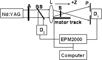
The crystal structures of samples were determined by an x-ray diffractometer (XRD; DX-2500 diffractometer, Fangyuan, China) with Cu Kα radiation (λ = 0.154145 nm) and its working current and voltage of 30 mA and 35 kV, respectively. The surface morphologies were determined by atomic force microscopy (AFM; SPA 400, Japan) and the cross-sectional micrographs of the thin films were examined by using a scanning electron microscope (SEM; JSM-5600LV JEOL, Japan). The optical transmittance spectra of the BLTN thin films were determined by UV–vis–NIR (near-infrared) spectrophotometer (Varian Cary-5000, USA) in the wavelength range from 200 to 800 nm. The nonlinear optical properties such as nonlinear refractive index and nonlinear absorption coefficient were determined using a single-beam Z-scan technique proposed by Sheik-Bahae et al.Reference Sheik-Bahae, Said, Wei, Hagan and VanStryland10 Measurements were carried out using a Q-switched Nd:YAG laser (Continuum, PY61C-10, USA) operated at 1064 nm as excitation source. Pulse width and repetition rate of the excitation source are 38 ps and 10 Hz, respectively. Figure 1 shows the Z-scan experiment setup. A convex lens with focal length f 1 = 260 mm was used to produce a focused laser beam. Its beam waist ω 0 for 1064 nm was 29.35 μm. A dual-channel energy radiometer and two energy detectors (EPM2000 and J3-05, respectively; Molectron, USA) were used to measure both the transmitted beam energy and the reference beam energy. A typical peak power density of 1.025 GW/cm2 was maintained throughout our work. The light intensities transmitted across the sample were measured as a function of the sample position in the z-direction with respect to the focal plane either through a small aperture (closed-aperture Z-scan) or without an aperture (open-aperture Z-scan). For closed-aperture Z-scan experiments, the linear transmittance of the far-field aperture, defined as the ratio of the pulse energy (μJ) passing the aperture to the total pulse energy (μJ), was measured to be 0.3. The measurement system was calibrated by using CS2 as a standard specimen.
Schematic diagram of the Z-scan experiment setup: A, attenuator; BS, beam splitter; L, lens; P, aperture; S, sample; D1, D2, detectors.

III. RESULTS AND DISCUSSION
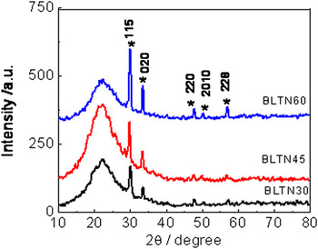
Figure 2 shows XRD patterns of BLTN-1.05 thin films. All the diffraction peaks indicated that the film completely crystallized into a single phase of Bi-layered perovskite structure without traces of any impurity phases. The peaks are indexed according to the standard powder diffraction data. Although there is excess 5 mol% Bi2O3 in the target, no Bi2O3 peak was observed. It means that the excess 5 mol% Bi ions in the starting materials compensate for the Bi evaporation during the preparation of BLTN-1.05 targets. With the increase in the deposition time, the intensities of all the peaks become stronger and sharper. It was found that the strongest diffraction peak grows along the (115) orientation. The broader peak near 22° comes from the fused-quartz substrate.
X-ray diffraction patterns of BLTN-1.05 thin films.

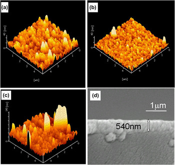
The surface morphologies of the films are important for optical applications. A rough surface leads to scattering losses, which can affect the actual nonlinear optical properties.Reference Chen, Gu, Cai, Xiong and Wang11 The surface and cross-sectional morphologies of the samples are shown in Fig. 3. The mean square root roughness of the spherical-shaped grains in the order of BLTN30, BLTN45, and BLTN60 is 6.27, 3.45, and 7.50 nm, respectively. It can be seen from Fig. 3 that BLTN30 and BLTN60 possess a roughened surface with some pores, and BLTN45 presents uniform surface and compact texture. Figure 3(d) shows that the thickness of BLTN45 was about 540 nm.
Atomic force microscopic images showing (a)–(c) surface morphology and (d) cross section of LBTN-1.05 thin films on fused quartz substrates.

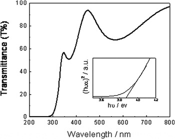
Figure 4 presents the optical transmittance spectrum of BLTN45 corrected for the attenuation of the fused quartz substrate. The film is highly transparent in the UV–vis region with a transmittance between 60 and 90%. The oscillations in transmittance spectrum come from the interference of reflected light from the top surface of the film and the interface between the film and substrate. The transmittance decreased drastically to zero at ∼297 nm. For light with a wavelength longer than 297 nm, the film shows good transparency. The inset of Fig. 4 exhibits the estimation of optical band gap of BLTN45. The linear absorption coefficient α and band gap energy E g could be related through (αhν)n = hν − E g, where ν is the frequency, h is the Plank’s constant, and n = 0.5 for indirect-band-gap material.Reference Mor, Varghese, Paulose, Shankar and Grimes12 The optical band gap energy of the BLTN45 is estimated to be about 3.87 eV from the graph of (αhν)2 versus hν. The linear index n 0 and linear absorption coefficient α of the thin films can be estimated using the envelope approach to be equal to 2.288 and 4.5 × 10⁻⁴ cm−1,Reference Du, Zhang, Wu, Kang, Yang, Wu and Yin13 respectively.
Optical transmittance of LBTN45 deposited on the fused quartz substrate. The inset is a plot of (hυα)2 versus hυ.

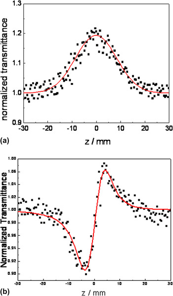
Figure 5(a) shows the normalized open aperture transmittance of BLTN45 on the fused quartz substrate. A symmetric bell-shaped transmission with a maximum at the focus (z = 0) indicated the presence of nonlinear saturation absorption. When linear absorption is negligible, the nonlinear absorption coefficient β (m/W) can be obtained by fitting the open aperture Z-scan experimental data with the following equationReference Sheik-Bahae, Said, Wei, Hagan and VanStryland10:

Normalized transmittance of BLTN45 for (a) open aperture and (b) closed aperture Z-scan.

where z is the position of the sample and z 0 = 2πω 02/λ is Rayleigh range of the beam, L eff = [1 − exp(−αL)]/α is the effective thickness of the film, L is the real film thickness, α is the linear absorption coefficient of the film, and I 0 is the on-axis laser intensity at the focal point. The fitting gives the nonlinear absorption coefficient β = −7.48 × 10⁻⁸ mw−1, which is larger than Bi1.95La1.05TiNbO9(5.95 × 10⁻⁸), Bi3.25La0.75Ti3O12(−6.76 × 10⁻⁸), and (Na0.9K0.1)Bi0.5TiO3 (6.59 × 10⁻⁹).Reference Chen, Yang, Zhang, Wang, Cheah and Cao9, Reference Zhang, Zhang, Chen and Yin14, Reference Prakash, Cazzanelli, Gaburro, Pavesi, Iacona, Franzo and Priolo15 The sign of β is opposite to the results of Chen et al.Reference Chen, Yang, Zhang, Wang, Cheah and Cao9 The imaginary part of the third-order nonlinear susceptibility Imχ (3) can be obtained from β according to the following equationReference Sheik-Bahae, Said, Wei, Hagan and VanStryland10:

where c is light speed in vacuum and n 0 is the linear refractive index of BLTN45. The Imχ (3) for the BLTN45 is −3.67 × 10⁻⁹ esu.
Figure 5b shows the normalized closed-aperture transmittance of BLTN45 on the fused quartz substrate. The solid line is the theoretical fitting. The signal profile with a valley followed by a peak indicates a positive (self-focusing) optical nonlinearity. To determine the third-order nonlinear susceptibility, the Z-scan data were analyzed using the procedures described in Ref. Reference Sheik-Bahae, Said, Wei, Hagan and VanStryland10. The normalized transmission of closed-aperture Z-scan curve is given by

where x = z/z 0, z is the longitudinal distance from the focal point, z 0 is the Rayleigh range of the beam, and ΔΦ0 is the on-axis phase shift at the focus. The normalized closed-aperture Z-scan data are fitted with Eq. (3) to obtain ΔΦ0 values. The nonlinear refractive index coefficient γ is then related to ΔΦ0 by the Eq. (4), and the nonlinear refractive index n 2 and the real part of the third nonlinear susceptibility Reχ (3) are given by the following equationsReference Sheik-Bahae, Said, Wei, Hagan and VanStryland10, Reference Shi, Yao, Zhang, Wu, Wang and Wan16:


The calculated γ value is 7.21 × 10⁻¹⁵ m2/w and n 2 = 3.93 × 10⁻⁸ esu. The real part Reχ (3) = 9.56 × 10⁻⁹ esu. As we all know, the magnitude of the nonlinear susceptibility that is expressed by  is 1.02 × 10⁻⁸ esu. The third-order nonlinear susceptibility χ (3) are larger than other materials, such as CdS, ZnSe, ZnTe, and LiNbO3:MgO.Reference Wang, Fu and Gu17–Reference Li, Kam, Lam and Ji19 As mentioned earlier, it is obvious that the real part of the third-order nonlinear susceptibility χ (3) is larger than the imaginary part, which indicates that the nonlinearity is dominated by the nonlinear refractive behavior.
The role of thermal nonlinearity in the study was negligible. The main requirements for the thermal effect to play an important role during the propagation of laser radiation through the medium are long pulse duration, high pulse repetition rate, and strong linear absorption. The accumulative thermal effect could play an important role in the case of picosecond and even femtosecond pulses only at high repetition rates (order of MHz). We used picosecond pulses (38 ps) with a low pulse repetition rate (10 Hz) so that the thermal effect could be neglected. Under the picosecond pulse duration and low repetition frequency laser in this experiment, only the electronic effect with the response time on the order of a picosecond in the sample contributes to nonlinear polarization or nonlinear refraction. When the linear absorption is negligible at 1064 nm, the mechanism of nonlinear saturable absorption in open aperture transmittance Z-scan is attributed to multi-photon absorption.
IV. CONCLUSIONS
In summary, BLTN thin films with bismuth-layered perovskite structure have been deposited on fused quartz substrates by PLD. BLTN45 exhibits higher crystalline quality and smoother surface. The nonlinear susceptibility is measured by using single-beam Z-scan setup with 38 ps laser pulses at 1064 nm. The Z-scan-normalized transmittance curve of BLTN45 showed saturation absorption. The nonlinear refractive index coefficient γ and the nonlinear absorption coefficient β of the thin film are 7.21 × 10⁻¹⁵ m2/w and −7.48 × 10⁻⁸ m/W, respectively. The third-order nonlinear optical susceptibility χ (3) of BLTN45 is 1.02 × 10⁻⁸ esu. The results show that BLTN ferroelectric thin films may be a promising nonlinear optical device material.
ACKNOWLEDGMENTS
This work was supported by The Science and Technology Department and The Education Department of Henan Province of China (Grant No. 082300460070 and 2008A140001).