Introduction
The recent surge of interest in oxide interfaces has been fueled by the possibility of stabilizing electronic ground states, leading to emerging properties. Many of these complex oxides share a common perovskite structure with similar lattice parameters that allow the growth of epitaxial interfaces with high structural perfection. At interfaces, electron correlations establish novel forms of coupling between electronic ground states of the adjoining materials, which have been proposed to be the origin of emergent properties. Reference Dagotto1 A paradigmatic case is the metallic state at the interface between two band insulators as in LaAlO3/SrTiO3 (LAO/STO) heterostructures. Reference Ohtomo and Hwang2 This finding triggered a new research field aimed at finding interesting novel phases at oxide interfaces with a high potential for applications. Reference Reyren, Thiel, Caviglia, Fitting Kourkoutis, Hammerl, Richter, Schneider, Kopp, Ruetschi, Jaccard, Gabay, Muller, Triscone and Mannhart3–Reference Bousquet, Dawber, Stucki, Lichtensteiger, Hermet, Gariglio, Triscone and Ghosez5
At interfaces, the important quantities controlling the nucleation of different electronic phases (charge density, electrostatic repulsion and bandwidth) may change substantially in a phenomenon called electronic reconstruction. Reference Okamoto and Millis6,Reference Mannhart and Schlom7 In addition, interface strain is also an important parameter controlling phase stabilization. Reference Tokura and Nagaosa8–Reference Garcia-Barriocanal, Bruno, Rivera-Calzada, Sefrioui, Nemes, Garcia-Hernandez, Rubio-Zuazo, Castro, Varela, Pennycook, Leon and Santamaria13 Oxides, as compared to other materials, are able to accommodate very large amounts of epitaxial strain without breaking into islands or structural domains. This is probably due to the large polarizability of the oxygen sublattice, Reference Mannhart and Schlom7 which admits quite large deformations in the form of rotations and distortions of the oxygen octahedra.
The possibility of tailoring electronic properties at oxide interfaces has raised the question of whether the properties of oxygen ion conducting materials could also be modified at interfaces. In this regard, the coherent growth of strained interfaces in heterostructures combining materials with different degrees of lattice mismatch has been shown to promote ion diffusivity Reference Garcia-Barriocanal, Rivera-Calzada, Varela, Sefrioui, Iborra, Leon, Pennycook and Santamaria14 and thus, these heterostructures may play an important role in the optimization of materials for electrochemical devices such as batteries and fuel cells that are key to commercially viable low power energy generation and storage. Reference Steele and Heinzel15,Reference Aricò, Bruce, Scrosati, Tarascon and van Schalkwijk16 In particular, enhanced oxide-ion conductivity at oxide interfaces would be relevant for lowering the operation temperature of solid oxide fuel cells (SOFCs). In SOFCs, O2– ions form at the cathode and diffuse through a solid electrolyte material at elevated temperatures (usually 800–1000°C) to react with H+ ions in the anode to produce water. The high operation temperatures favor internal fuel reformation, electrode processes, and ionic migration through the electrolyte, but impose serious restrictions on materials selection due to thermal stress or fatigue. Thus, a major materials research goal today is to reduce the operating temperature of SOFCs without compromising device performance. Reference Steele and Heinzel15 Novel electrolytes are needed with higher oxide-ion conductivity and also electrode materials with higher oxygen exchange rates.
Materials synthesis strategies based on chemical substitutions to increase the concentration of mobile species have limitations, and increasing conductivity beyond the values corresponding to optimal concentrations requires increasing the operation temperature. Reference Aricò, Bruce, Scrosati, Tarascon and van Schalkwijk16–Reference Etsell and Flengas18 A different strategy to find materials with higher ionic conductivity is to exploit the conductivity increases that result from size effects, when (one or more) sample dimensions are reduced down to the nanometer scale. Nanotechnology is expected to have a large impact on the next generation of fuel cells since ionic transport can be strongly modified in nanomaterials. Reference Maier19–Reference Tuller21 The term nano-ionics has been coined to embrace the new concepts in ion transport and electrochemical storage resulting from nanoscale effects. Reference Maier22
In this article, we review recent results of enhanced oxygen ion conductivity at oxide interfaces as well as the theoretical scenarios being considered to explain it. In particular, space-charge effects, which might account for changes in the carrier density, and epitaxial strain, which might tailor an enhanced mobility pathway for the ions, are revised. The atomic reconstruction occurring at interfaces between complex oxides is also discussed as a source of unexpected changes in the interface chemistry, where the mismatch in the bonding or polar structure of the layers might play a leading role. A final section is devoted to oxygen surface exchange, which may also be strongly enhanced at interfaces, signaling a new route toward novel artificial electrode materials in solid oxide fuel cells.
Space-charge effects
It is well established that the energy required for defect generation may be different at surfaces or boundaries. The discontinuity of free energy at interfaces naturally results in charge transfer processes that break charge neutrality and may profoundly change the carrier density. In ionic compounds, the accumulation of defects creates an electric field that is screened over a space-charge layer (the spatial extent of the electric field), by depletion or accumulation of mobile charges, and whose characteristic length scale is the Debye length, the length scale of charge inhomogeneities. Reference Kliewer and Koehler23 Space-charge effects are known to give rise to interesting nano-ionic size effects emerging when the extension of the space-charge region is comparable to sample dimensions. Reference Maier24–Reference Maier26 Quite remarkable is the large enhancement of the electronic conductivity discovered in mixed ionic-electronic conductor CeO2 nanocrystalline samples, in the pioneering work by Tuller and co-workers, measured by impedance spectroscopy and discussed in terms of accumulation of vacancies at the grain boundary cores. Reference Chiang, Lavik, Kosacki, Tuller and Ying27 Maier and colleagues Reference Sata, Eberman, Eberl and Maier28 have broken new ground in nano-ionics, showing a large increase in ionic conductivity in layered thin-film BaF2/CaF2 superlattices as a result of an interfacial effect resulting from the transfer of fluorine ions into the CaF2 side due to the electrochemical potential gradient across the interface. This yields enhanced vacancy concentration in the Ba side when the thickness of the individual layers become comparable to the size of the space-charge region (i.e., of tens of nanometers).
Following the work by Maier et al., there were some controversial results on the occurrence of space-charge effects at the interfaces of oxide-ion conductors, such as yttria-stabilized zirconia (YSZ), x Y2O3: (1–x) ZrO2. Among oxide-ion conductors, those of the anion-deficient fluorite structure such as YSZ are extensively used today as electrolytes in SOFCs. Reference Steele and Heinzel15,Reference Chadwick17 Doping with Y2O3 is known to stabilize the cubic fluorite structure of ZrO2 at room temperature and simultaneously supply oxygen vacancies responsible for its ionic conductivity. Reference Etsell and Flengas18 Some authors reported increases in ionic conductivity in nano-granular samples, Reference Kosacki, Suzuki, Petrovsky and Anderson29 while others found no changes Reference Peters, Weber, Ivers-Tiffee, Störmer, Gerthsen, Bockmeyer and Krüger30 or even decreases Reference Mondal and Hahn31,Reference Jiang32 in conductivity. Reference Etsell and Flengas18 O tracer diffusion experiments assisted by secondary ion mass spectroscopy also yielded contradictory results: While a three orders of magnitude increase in the diffusion coefficient as compared with bulk samples was reported in nanocrystalline thin films, Reference Knoener, Reinemann, Roewer, Soedervall and Schaefer33 bulk nanocrystalline ceramics showed no change. Reference De Souza, Pietrovski, Anselmi-Tamburini, Kim, Munir and Martín34
It was also not straightforward to explain the observed increases due to a space-charge effect, because the Debye screening length in these materials is very short, on the order of 0.1 nm for typical dopant concentrations (8% YSZ) at intermediate temperatures (500°C). However, the possibility of enhanced ionic conductivity in nanostructures triggered large activity in the field, mainly due to its impact in the design of electrolytes with lower operation temperatures Reference Litzelman, Hertz, Jung and Tuller35 or in electrodes with higher oxygen exchange rates. Reference Steele36 Tuller and colleagues Reference Kosacki, Gorman, Anderson, Ramanayanaran, Worrell, Tuller, Kandkar, Morgensen and Gopel37 found a two orders of magnitude increase in the high temperature ionic conductivity of thin films of YSZ deposited by spin coating on Al2O3 when their thickness was reduced to the 10 nm range.
Later, Kosacki et al. Reference Kosacki, Rouleau, Becher, Bentley and Lowdness38 also reported a large increase in the conductivity of 10% Y2O3 doped YSZ epitaxial thin films grown on MgO when thickness was reduced down to 15 nm. The conductivity increase, of more than two orders of magnitude at 400°C, was accompanied by a reduction in the activation energy down to 0.62 eV. The authors attribute the conductivity increase to a highly conducting 1 nm layer at the YSZ/MgO interface. Karthikeyan et al. Reference Karthikeyan, Chan and Ramanathan39 found a more moderate conductivity increase of one order of magnitude for 17-nm-thick YSZ polycrystalline multiphase samples grown on MgO.
On the other hand, Guo et al. Reference Guo, Vasco, Mi, Szot, Wachsman and Waser40 found a decrease in the ionic conductivity of 12-nm-thick nanostructured polycrystalline YSZ thin films deposited on MgO as compared to 8% Y2O3 doped bulk ceramics and essentially no change in the activation energy, suggesting that epitaxial growth is an important step in attaining enhanced ionic mobility. In fact, a number of papers have reported increased conductivity of fluorite-based heterostructures and superlattices associated with the increased migration volume resulting from misfit dislocations at the interface. Reference Azad, Marina, Wang, Saraf, Shutthanandan, McCready, El-Azab, Jaffe, Englehard, Peden and Thevuthasan41–Reference Korte, Peters, Janek, Hesse and Zakharov44 This indicated that enhanced conductivity at epitaxial interfaces involving nanometer-thick YSZ may arise not only from space-charge effects but also from epitaxial strain or atomic reconstruction reported to appear at interfaces between correlated oxides. Reference Ohtomo, Muller, Grazul and Hwang45,Reference Thiel, Hammerl, Schmehl, Schneider and Mannhart46
Epitaxial strain
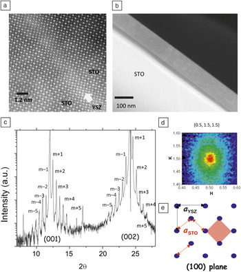
Motivated by these previous reports, and in an attempt to isolate a true interface effect on ion conductivity in oxide heterostructures, Garcia-Barriocanal et al. Reference Garcia-Barriocanal, Rivera-Calzada, Varela, Sefrioui, Iborra, Leon, Pennycook and Santamaria14 grew highly strained multilayers combining STO and ultrathin YSZ layers with controlled thickness down to the unit cell level (0.3–1 nm) (see Figure 1 ). They found conductivity values from dielectric spectroscopy measurements as large as eight orders of magnitude higher than bulk YSZ conductivity values at room temperature, which they attributed to enhanced oxide-ion conductivity. Reference Garcia-Barriocanal, Rivera-Calzada, Varela, Sefrioui, Iborra, Leon, Pennycook and Santamaria14 The DC conductivity determined from the low frequency plateau of conductivity spectra was independent of the YSZ layer thickness, which was taken as an indication of its interfacial origin.
(a) Z-contrast STEM image of an epitaxial 1-nm-thick YSZ layer (marked by the arrow) between 10 nm STO layers in a [YSZ1 nm /STO10 nm ]9 superlattice (with nine repeats). (b) Low magnification image of the same superlattice. (c) Synchrotron x-ray diffraction (λ = 0.855 Å) pattern obtained at the beam line BM 25 of the European Synchrotron Radiation Facility (ESRF) of a 1 nm YSZ/10 nm STO superlattice with 20 bilayer repetitions. (d) Reciprocal space map referring to the STO structure in the 0.5, 1.5, 1.5 position. (e) Sketch showing that the lattice parameters of YSZ and STO in the (001) plane allow a coherent growth of YSZ layers despite a 7% tensile strain. Figure adapted with permission from References 14 and 65.

Guo has proposed Reference Guo47 the electronic origin of the large conductivity values found in this experiment, but the possibility that the enhanced conductivity originated in electron doping of the substrate or STO layers was eliminated by measuring the DC (electronic) contribution of the conductivity, which turned out to be almost three orders of magnitude smaller than the global conductivity measured with AC methods. Reference Garcia-Barriocanal, Rivera-Calzada, Varela, Sefrioui, Iborra, Leon, Pennycook and Santamaria48 DC ionic conductivity is thermally activated according to the following expression,
 $${\rm{\sigma }}_{dc} = {{4{\rm{\alpha }}e^2 a^2 {\rm{\nu }}_0 Ne^{S/k_{\rm{B}} } } \over {k_{\rm{B}} }}e^{ - E_A /k_{\rm{B}} T} $$
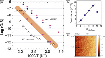
where α is a geometrical factor, a is the jump distance, ν0 is the attempt frequency, N is the concentration of oxygen vacancies, S is a configurational entropy term, e is the electron charge, k B is the Boltzmann constant, and E A is the activation energy. Garcia-Barriocanal et al. Reference Garcia-Barriocanal, Rivera-Calzada, Varela, Sefrioui, Iborra, Leon, Pennycook and Santamaria14 discussed the conductivity enhancement in terms of a decrease in the activation energy from values of about 1 eV for bulk samples to 0.6 eV for ultrathin trilayers (see Figure 2 a) and of the large conductivity pre-exponential factor of the STO/YSZ/STO trilayer samples, which may result from an increase in the concentration of oxygen vacancies, and/or a large entropy term related to disorder. Reference Garcia-Barriocanal, Rivera-Calzada, Varela, Sefrioui, Diaz-Guillen, Moreno, Diaz-Guillen, Iborra, Fuentes, Pennycook, Leon and Santamaria49
(a) Arrhenius plot for the conductance, G, in Siemens (S), of a [YSZ1 nm/STO10 nm]4 superlattice (stars) and a STO10 nm/YSZ1 nm/STO10 nm trilayer (circles) with 100-oriented YSZ layers compared to that of a STO20 nm film (squares) and a bare STO substrate (triangles). The colored band represents the conductance range of [YSZ1 nm/STO10 nm] superlattices and trilayers of several different thicknesses and with 110-oriented YSZ layers. (b) Conductance at 400 K of [YSZ1 nm/STO10 nm]ni/2 superlattices (with ni/2 repeats) as a function of the number of interfaces ni. (c) AFM image of a 1 nm-thick YSZ layer grown on TiO2 terminated 0.1% wt. Nb doped STO. It shows well-defined steps one unit cell high separating vicinal terraces that indicate a two-dimensional growth mode. Figure adapted with permission from References 14 and 65.

A reduction in the activation energy for oxygen ion diffusion has been obtained from an ab initio-based kinetic Monte Carlo model for ionic conductivity in YSZ. Reference Lee, Prinz and Cai50 Ionic interactions are found to be essential to reproduce the effective activation energy, Reference Ngai51 and the enhanced oxygen ion mobility may result from a non-random distribution of dopant Y ions at the interfacial planes, Reference Lee, Prinz and Cai50 structural disorder, Reference Sankaranarayanan and Ramanathan52 or from a decrease in ionic interactions when the layer thickness goes down to the nanometer range. Reference Ngai, Santamaria and Leon53 An important point might be the effect of epitaxial strain on defect association, which in YSZ is known to immobilize oxygen vacancies at temperatures lower than 1000 K. Hence, the conductivity is controlled by both the mobility and the defect association constant. Generally, it is believed that associates are formed between yttrium in zirconium sites and oxygen vacancies (Yzr ’ and Vo¨ in Kröger–Vink notation), although oxygen vacancies could also be immobilized by a strain field due to the size difference between Zr4+ and Y3+ cations. Reference Norberg, Hull, Ahmed, Eriksson, Marrocchelli, Madden, Li and Irvine54 An interesting possibility is that the apparent mobility could increase significantly when this strain field is alleviated by an externally induced strain (although not by several orders of magnitude).
Other authors have also reported substantial enhancement of the ionic conductivity (though smaller than in Reference 14) in ultrathin epitaxial YSZ layers. Sillassen et al. Reference Sillassen, Eklund, Pryds, Johnson, Helmersson and Bottiger55 reported a more than three orders of magnitude enhancement of oxide-ion conductivity at low temperatures (lower than 350°C) in epitaxial YSZ films grown on MgO substrates. Their results also indicate that the observed enhancement is due to an interfacial effect and related to a combination of misfit dislocation density and elastic strain in the interface. The importance of epitaxial strain in determining the increase in ionic conductivity at oxide interfaces and nanolayers has been very recently addressed experimentally by several groups. Janek et al. Reference Schichtel, Korte, Hesse and Janek56 reported on the influence of strain on ion conduction at oxide interfaces, finding small conductivity enhancements in pulsed laser deposition (PLD) grown samples with partially coherent or non-coherent interfaces. Hertz et al. Reference Jiang, Hu, Shen, Ni and Hertz57 have reported improved oxide-ion conductivity in ultrathin films of YSZ (below 10 nm thickness) grown by sputtering on Al2O3 substrates. There is an increase in the out-of-plane lattice parameter in these films due to tensile strain, which may assist in-plane ionic conduction. Lian et al. Reference Li, Zhang, Kaspar, Shutthanandan, Ewing and Lian58 have reported a two orders of magnitude increase in oxide-ion conductivity, as compared with bulk YSZ, in YSZ/Gd2Zr2O7 heterostructures with 3% tensile strain and dislocation-free interfaces upon the manipulation of the layer thickness down to 5 nm.
Hyodo et al. Reference Hyodo, Ida, Kilner and Ishihara59 studied Pr2Ni0.71Cu0.24Ga0.05O4/Sm0.2Ce0.8O2 layer-by-layer nano-sized laminated films and found a significant increase in oxide-ion conductivity compared to values for bulk samarium doped ceria (SDC); they proposed this to be due to the expanded lattice of SDC in these heterostructures. Janek et al. Reference Aydin, Korte, Rohnkea and Janek60 have reported an enhancement of 18O tracer diffusion coefficient for transport along strained YSZ films in YSZ/Y2O3 multilayer samples. From the functional course of the measured mean oxygen ion diffusion coefficient versus layer thickness between 12 and 45 nm, they estimated an elastically strained interface region thinner than 5 nm with modified ionic transport properties.
One has to be careful interpreting impedance measurements when using active electrodes such as Ag or Pt. Gold is a better option to block oxygen ions. Reference Badwal, Bannister and Murray61 Furthermore, surface diffusion (conduction) could influence measurement of the in-plain conductivity of thin films. The critical point about enhanced oxygen-ion conductivity is proven by 18O-exchange experiments, preferably under current flow. There are also some controversial results regarding conductivity enhancement of epitaxially strained layers. Pergolesi et al. Reference Pergolesi, Fabbri, Cook, Roddatis, Traversa and Kilner62 studied YSZ-CeO2 heterostructures on MgO substrates, where interfaces were found to be non-uniformly but significantly strained, and they reported no detectable contribution to the total conductivity even in the case of layers as thin as about 10 unit cells. Fleig et al. Reference Gerstl, Friedbacher, Kubel, Hutter and Fleig63 grew, by using PLD, YSZ layers with larger thickness ranging from 30 to 300 nm onto MgO, Al2O3, and SrTiO3 substrates with different lattice parameters, and they did not find an enhancement in ionic conductivity. They attribute this result to the presence of grain boundaries in the films that strongly block ion transport. Cavallaro et al. Reference Cavallaro, Burriel, Roqueta, Apostolidis, Bernardi, Tarancón, Srinivasan, Cook, Fraser, Kilner, McComb and Santiso64 have grown YSZ/STO heterostructures using PLD and found that the layers were discontinuous, and YSZ islands had mixed crystalline orientations. They found enhanced values of the electronic conductivity that they attributed to an interfacial alloyed oxide resulting from zirconium/strontium intermixing. These results suggest the possible importance of crystalline orientation of the YSZ growth in order to obtain coherent, epitaxial films with enhanced ionic conductivity.
By using different temperatures during the growth of YSZ films on STO using a sputtering technique, Rivera-Calzada et al. Reference Rivera-Calzada, Diaz-Guillen, Dura, Sanchez-Santolino, Pennycook, Schmidt, Bruno, Garcia-Barriocanal, Sefrioui, Nemes, Garcia-Hernandez, Varela, Leon, Pantelides, Pennycook and Santamaria65 were able to control the crystalline orientation that allowed stabilizing different morphologies, layer continuity, and epitaxy and, as a result, different degrees of ion mobility enhancement (see Figure 2). 〈001〉 YSZ growth yields coherent interfaces despite the 7% mismatch between the two highly dissimilar structures, stabilizing a disordered oxygen sublattice with an increased number of accessible positions for oxygen that promote oxygen diffusion. On the other hand, the 〈110〉 YSZ orientation results in the growth of connected islands, whose boundaries block the long range diffusion of ions. Moreover, conductance of superlattices with coherent interfaces scaled with the number of interfaces and is evidence that enhancement of ion conductivity is an interfacial effect (see Figure 2). These results show that epitaxial strain is an important parameter in designing a high mobility landscape at interfaces in addition to space-charge effects. Reference Fabbri, Pergolesi and Traversa66,Reference Rupp67
In fact, several theoretical groups have proposed that epitaxial strain provides an avenue to increase the conductivity of ion-conducting solids, and understanding its effects and uncovering the microscopic mechanism has become an important challenge. Reference Ngai, Santamaria and Leon53,Reference Schichtel, Korte, Hesse and Janek56,Reference Korte, Schichtel, Hesse and Janek68–Reference Pennycook, Oxley, Garcia-Barriocanal, Bruno, Leon, Santamaria, Pantelides, Varela and Pennycook74 One important direction has been the use of static models to evaluate changes in the migration volume. Korte and co-workers, using a qualitative model of ion diffusion along heterointerfaces based on the increased activation volume associated with the density of misfit dislocations and interfacial strain, have pointed out that strain by itself can only account for two to three orders of magnitude conductivity increase in YSZ/STO heterostructures. Reference Schichtel, Korte, Hesse and Janek56,Reference Korte, Schichtel, Hesse and Janek68 This model predicts a linear increase of the conductivity with lattice mismatch for tensile strained interfaces, while compressive strain will decrease the ionic conductivity.
On the other hand, de Souza and colleagues Reference De Souza, Ramadan and Hörner72,Reference Hintenberg, Zacherle and de Souza73 made use of static lattice simulation techniques using phenomenological potentials to describe the long range Coulomb interaction and the short range forces arising from electron cloud overlap. Lattice relaxation is performed over several hundreds of neighboring ions surrounding the migrating species. The effect of strain affects the free energy for migration through its effect on the free migration volume. This model would account for a conductivity increase up to five orders of magnitude using the experimental values of the activation energy in YSZ/STO heterostructures by Garcia-Barriocanal et al. Reference Garcia-Barriocanal, Rivera-Calzada, Varela, Sefrioui, Iborra, Leon, Pennycook and Santamaria14 It is concluded that lattice strain alone cannot be responsible for the total conductivity increase found experimentally. Reference De Souza, Ramadan and Hörner72 Furthermore, a recent paper by Yildiz and collaborators Reference Kushima and Yildiz70 examined the effect of biaxial strain on oxygen diffusivity using combined density functional theory (DFT) calculations and kinetic Monte Carlo simulations and concluded that bond reconfiguration poses an upper limit to the effect of epitaxial strain in enhancing the conductivity by expanding the conduction path.
A potential problem with these models is that they tackle the issue of epitaxial strain by stressing bulk structure (i.e., they do not explicitly include the presence of interfaces, which may incorporate interesting ingredients related to the chemical and structural compatibility of the merging lattices). Density-functional calculations have been used to investigate the influence of the (001)-oriented interface on the conductivity increase in YSZ/STO superlattices explicitly considering the presence of the interface by introducing mixed YSZ/STO supercells. Reference Pennycook, Beck, Varga, Varela, Pennycook and Pantelides69 The authors of that work proposed that the combination of epitaxial strain and oxygen sublattice incompatibility between the two structures are key in yielding the highly conducting interface. They reported that 7% strain produces a drastic change in the O sublattice of YSZ, which becomes as disordered as expected from an increase in temperature up to 2000 K. The O ion mean square displacement (mobility) is strongly enhanced (by a factor of over 106) as a result of the combined presence of oxygen vacancies and disorder. The incompatibility of the oxygen positions in the interface planes (octahedral in STO versus tetrahedral in YSZ) are proposed to play a key role in stabilizing the highly conducting interface by introducing extreme disorder in the oxygen sublattice in the region close to the interface. Electron energy loss spectroscopy (EELS) experiments (both spectroscopy and imaging) have provided evidence for the oxygen disorder. Reference Pennycook, Oxley, Garcia-Barriocanal, Bruno, Leon, Santamaria, Pantelides, Varela and Pennycook74 Moreover, density-functional simulations show that a new YSZ phase is stabilized in epitaxially strained heterostructures for mismatch strain levels in excess of 5.2%. Reference Pennycook, Beck, Varga, Varela, Pennycook and Pantelides69 This result explains why these high levels of strain do not result in strain relaxation by mismatch dislocations and islanding, and provides evidence for the lattice relaxation playing a dominant role in phase stabilization.
Very recently, Li et al. Reference Li, Lu, Wu, Kan, Xiao, Deng and Ellis75 performed DFT and first-principles molecular dynamics simulations to examine the strain effect on oxygen conductivity in a KTaO3/YSZ/KTaO3 sandwich structure with 9.7% lattice mismatch. They found a large decrease in activation energy for ionic conduction, and estimated the oxygen ionic conductivity for KTO-strained zirconia to be 6.4 × 10⁷ times higher than that of the unstrained bulk zirconia at 500 K. Interestingly, by using Al2O3 and SrTiO3 instead of KTaO3 in the simulations, a nearly linear relationship is identified between the energy barrier and the lattice mismatch in the sandwich structures in that work.
Atomic reconstruction at the interface
Aside from epitaxial strain, polarity mismatch may play an important role in determining the atomic reconstruction at the interface and may cause a departure from stoichiometry, which may be the source of increased density of (ionic) charge carriers. In the well-known case of the LAO/STO interface, the nonpolar STO (100) planes ((TiO2)0– (SrO)0– (TiO2)0– . . . ) match the polar LAO (100) planes ((AlO2)–(LaO)+– (AlO2)–. . . ), which causes a divergence in the electrostatic energy when the LAO thickness increases. In the polar catastrophe scenario, Reference Nakagawa, Hwang and Muller76 electronic charge is transferred from the LAO surface to the interface, where Ti is partially reduced from 4+ to 3+, yielding a conducting interfacial state. This charge transfer process avoids the divergence of the electrostatic potential and identifies polarity mismatch as an important driving force in electronic reconstruction. Reference Ohtomo and Hwang2–Reference Mannhart and Schlom7,Reference Nakagawa, Hwang and Muller76
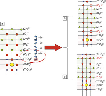
It is worth noting that other processes have been proposed to originate the conducting state at the interface, such as formation of oxygen vacancies or intermixing, which might also originate at the polarity mismatch. There is also a strong polar discontinuity at the interfaces between ion conducting materials discussed in this work. For example, in the case of (100) YSZ/STO superlattices, the nonpolar STO (100) planes alternate with strongly polar YSZ (100) planes with a sequence (Zr)4+– (O2)4–(Zr)4+– …. This plane sequence is the source of a very energetically unstable situation, which cannot be settled by electron transfer to the interface in the case of symmetric TiO2-terminated STO interfaces shown by experiment Reference Garcia-Barriocanal, Rivera-Calzada, Varela, Sefrioui, Iborra, Leon, Pennycook and Santamaria14 (see Figure 3 a). An interesting possibility is that oxygen vacancies nucleate at the interface (one oxygen vacancy per every interface unit cell) to avoid polarity mismatch and to restore charge neutrality (see Figure 3b). This may be an additional source (other than the incompatibility between perovskite and the fluorite unit cell) to justify the nucleation of a large number of oxygen vacancies at YSZ/STO interfaces. Another possibility is the formation of a (ZrO)2+ plane with a rock salt structure, as proposed recently by Dyer et al. Reference Dyer, Darling, Claridge and Rosseinsky77 from theoretical arguments (see Figure 3c). This interface termination is consistent with experimental observations and also preserves charge neutrality in the symmetrically terminated YSZ layer and avoids polarity mismatch. This reconstruction may in fact be related to the proposed zirconate interfacial compound proposed recently by Cavallaro and collaborators. Reference Cavallaro, Burriel, Roqueta, Apostolidis, Bernardi, Tarancón, Srinivasan, Cook, Fraser, Kilner, McComb and Santiso78
Sketches showing (a) the plane sequence for the growth of (100) YSZ/STO superlattices, with nonpolar STO (100) planes alternating with strongly polar YSZ (100) planes; (b) the nucleation of oxygen vacancies at the interface to avoid polarity mismatch and to restore charge neutrality; and (c) the formation of an (ZrO)2+ plane with rock salt structure that also preserves charge neutrality in the symmetrically terminated YSZ layer and avoids polarity mismatch.

In a related context, Ramanathan et al. Reference Ngai, Santamaria and Leon53 have shown, from molecular dynamics simulations, that in YSZ films on MgO substrates, there is a slight enrichment of dopant (i.e., yttrium at the YSZ free surface compared to the YSZ–MgO interface), and the extent of dopant enrichment is greater for lower thickness YSZ films. As a result, the interfacial conductivity increases by two orders of magnitude as the YSZ film size decreases from 9 to 3 nm, owing to a decrease in activation energy barrier from 0.54 to 0.35 eV in the 1200–2000 K temperature range. In summary, apart from epitaxial strain, atomic reconstruction arising at interfaces as the result of polarity mismatch or other forms of chemical incompatibility may be the source of modified coordination and stoichiometry at epitaxial interfaces, which may be important to understand modified ionic conductivity.
Oxygen surface exchange
Finally, a different scenario where oxide interfaces have recently shown their potential in connection with new materials for energy applications is oxygen exchange. In current SOFCs, if the conductance of the electrolyte is increased, either by increasing its conductivity or by reducing its thickness, electrode polarization losses become the dominant cause in limiting device performance. Reference Wachsman and Lee79 The slow kinetics of the thermally activated oxygen reduction reaction at the cathode is responsible for a good part of the resistive losses of current oxide fuel cells and is in fact one of the factors critically limiting their operation at lower temperatures. Reference Fleig80 At the cathode, O2 from the air is reduced, and O2– cations are transported through the electrolyte to the anode where they react with the gaseous fuel, releasing electrons to the external circuit. The use of mixed electronic-ionic cathode materials along with surface treatments Reference Kubicek, Limbeck, Frömling, Hutter and Fleig81 and optimization of the surface microstructure Reference Adler82,Reference Peters, Weber and Ivers-Tiffee83 has resulted in one order of magnitude enhancement of the exchange activity.
Epitaxial strain has been revealed to be a very effective parameter in accelerating oxygen exchange, Reference Burriel, Garcia, Santiso, Kilner, Richard and Skinner84,Reference Ji, Hwang, Yoon, Son, Kim, Lee and Lee85 and its role in surface chemistry and ion exchange has been a recent focus of great interest. First-principles calculations have shown that epitaxial strain favors oxygen vacancy formation in LaCoO3, Reference Kushima, Yip and Yildiz86 a well-studied fuel cell cathode, as well as results in enhanced oxygen mobility. Reference Han and Yildiz87 Sase et al. Reference Sase, Yasgiro, Sato, Mizusaki, Kawada, Sakai, Yamaji, Horita and Yokokawa88 have shown that oxygen surface exchange in the La0.6Sr0.4CoO3/(La, Sr)2 CoO4 heterointerface is increased by three orders of magnitude as compared to single cobaltite surfaces. The result is interpreted in terms of enhanced mobility at the interface connected with local strains. Jalili et al. Reference Jalili, Han, Kuru, Cai and Yildiz89 have shown that quite significant chemical modifications occur at the surface of La0.7Sr0.3MnO3 epitaxial films resulting from strain, namely Sr enrichment and enhanced oxygen vacancy formation. Using tracer diffusion experiments with isotopically modified 18O, Kubicek and collaborators Reference Kubicek, Cai, Ma, Yildiz, Hutter and Fleig90 have evidenced faster surface exchange (by a factor of 4) and enhanced surface diffusion (by a factor of 10) in tensile strained La1–x Sr x CoO3–δ layers grown on STO as compared to compressively strained ones grown on LAO. These effects are due to enhanced (oxygen) diffusion through reduced activation barriers for diffusion and/or energy (enthalpy) for oxygen vacancy formation. Reference Kubicek, Cai, Ma, Yildiz, Hutter and Fleig90 Also, very recently, Prinz et al. found a fivefold increase in the oxygen surface exchange coefficient of single-crystal YSZ on optimizing the dopant concentration at the surface with the help of atomic layer deposition of a 5–10 nm YSZ layer. Reference Chao, Park, Tian, Shim, Gür and Prinz91 The results demonstrate the potential of oxide interface engineering between an electrolyte and electrode to optimize the performance of SOFCs or other electrochemical devices.
Summary and outlook
An interesting new facet of oxide interfaces has been recently uncovered in connection with materials for energy applications. The enhanced ionic conductivity found in heterostructures involving solid electrolytes may impact the performance of oxide-based energy generation and storage devices. In particular, they could provide an avenue to reduce the high operation temperatures of current solid oxide fuel cells, which impose severe constraints on materials selection and durability of devices compromised by thermal fatigue. The important limiting factors are the oxygen conductivity through the electrolyte and the oxygen exchange rate at the electrodes, both of which can be drastically improved at oxide interfaces. Epitaxial growth of the heterostructures seems to play an important role in determining the increase in the ionic conductivity. While there is solid evidence for enhanced ion mobility in epitaxial oxide ultrathin layers or interfaces, a polycrystalline structure or non-homogeneous strain distribution seems to suppress this enhancement. However, the ultimate reason for the enhanced conduction at oxide interfaces remains to be elucidated, and different scenarios have been proposed as being relevant to explain experimental data: (1) charge transfer and space-charge effects, (2) effect of epitaxial strain in opening diffusion paths, and (3) interface atomic reconstruction in stabilizing new phases with increased carrier concentration.
These experimental findings have also triggered a growing theoretical effort aimed at understanding the enhanced conductivity in strained layers. It is important to confront the results of the models that explicitly consider the presence of the interface with those examining the effect of modified bulk structures. Ultimately, understanding the mechanism underlying enhanced ion diffusivity at oxide interfaces should help in selecting suitable materials and designing appropriate nanostructures for future energy devices based on oxide nanolayers.
Acknowledgments
The authors thank the financial support of the Spanish MICINN through Grant MAT2011–27470-C02, Consolider Ingenio 2010—CSD2009–00013 (Imagine), and by CAM through Grant S2009/MAT-1756 (Phama).