


Introduction
Hybrid inorganic–organic perovskites have set the materials science world abuzz because their solar cells have reached 20.1% efficiency[Reference Green, Emery, Hishikawa, Warta and Dunlop1] after fewer than 5 years of widespread research. Perovskites began as an alternative sensitizer for dye-sensitized solar cells (DSSCs),[Reference Kojima, Teshima, Shirai and Miyasaka2] but their superior charge-transport properties allowed the absorbing layer to thicken. Current mesostructured architectures still feature the perovskite absorber deposited on mesoporous TiO2,[Reference Kim, Lee, Im, Lee, Moehl, Marchioro, Moon, Humphry-Baker, Yum, Moser, Grätzel and Park3] but these same excellent charge-transport properties in the perovskite also prompted study of a thin-film version of the solar cell (Fig. 1), which yields similarly high efficiencies.[Reference Liu, Johnston and Snaith4]
Comparison of the mesoporous (left) and planar (right) architectures used in perovskite solar cells. Most devices with high efficiency use glass/FTO/TiO2/CH3NH3PbI3/Spiro-OMeTAD/Au. Except for the glass substrate, layer thicknesses are drawn approximately to scale.

The dramatic rise of perovskites in photovoltaics has caught the attention of scientists across many fields, and the initial hype has been bolstered by investigations of perovskites’ structural, optical, and electronic properties. Perovskites offer a combination of the characteristics of inorganic and organic semiconductors: the chemical tunability of their optoelectronic properties and low-temperature and solution-based deposition recall organics; their relatively high carrier mobility, diffusion length, and radiative lifetime more resemble those of polycrystalline semiconductors (Table I). These attractive properties have inspired dreams well beyond photovoltaics, and research in sunlight-to-fuel conversion,[Reference Luo, Im, Mayer, Schreier, Nazeeruddin, Park, Tilley, Fan and Gratzel5] light-emitting diodes,[Reference Tan, Moghaddam, Lai, Docampo, Higler, Deschler, Price, Sadhanala, Pazos, Credgington, Hanusch, Bein, Snaith and Friend6, Reference Kim, Cho, Heo, Kim, Myoung, Lee, Im and Lee7] lasers,[Reference Deschler, Price, Pathak, Klintberg, Jarausch, Higler, Hu, Leijtens, Stranks, Snaith, Atatu, Phillips and Friend8–Reference Zhang, Ha, Liu, Sum and Xiong10] and photodetectors[Reference Lee, Kwon, Hwang, Ra, Yoo, Ahn, Park and Cho11, Reference Dou, Yang, You, Hong, Chang, Li and Yang12] is already underway.
Comparison between CH3NH3PbI3-based perovskites and other photovoltaic technologies. Perovskites have many of the advantages of polycrystalline semiconductors such as CIGS and CdTe, but they are processed from solution-like organic materials or quantum dots. Material characteristics refer to values measured for materials similar to those used in the highest performing solar cells
* Under AM 1.5, 100 mW/cm2; † At 300 K in the vicinity of the band edge; ‡ Of the minority carrier (c-Si, GaAs, CIGS, CdTe, perovskite) or the exciton (dye-sensitized, organic, quantum dot); § E G–qV oc (band gap—open circuit voltage); ∥ Period at which the efficiency becomes 80% of the initial value; ¶ Corrected for photon-recycling effects; ** Of a dye in solution, not on TiO2; †† Of the donor–acceptor blends, not the pristine material.
a [Reference Green, Emery, Hishikawa, Warta and Dunlop1]. b Geist, J., Migdall, A., & Baltes, H. Appl. Opt. 27, 3777 (1988). c [Reference Kamins76]. d Modanese, C. et al. Prog. Photovolt: Res. Appl. 21, 1469 (2012). e Tiedje, T. et al. IEEE Trans. Electron Devices 31, 711 (1984). f Kegel, J. et al. Appl. Surf. Sci. 301, 56 (2014). g [Reference Blakemore78]. h Rey-Stolle, I. & Algora, C. Prog. Photovolt: Res. Appl. 11, 249 (2003). i Friedman, D.J., Olson, J.M., & Kurtz, S. High-efficiency III–V multijunction solar cells. (John Wiley & Sons, 2011). j Lumb, M. P. et al. J. Appl. Phys. 116, 194504 (2014). k [Reference Brown, Faifer, Pudov, Anikeev, Bykov, Contreras and Wu75]. l Chirilă, A. et al. Nature Mater. 12, 1107 (2013). m Repins, I. et al. Conference paper NREL/CP-520-46235 (2009). n Shah, A. et al. Science 285, 692 (1999). o [Reference Shin, Gunawan, Zhu, Bojarczuk, Chey and Guha74]. p Metzger, W.K., Repins, I.L., & Contrearas, M.A. Appl. Phys. Lett. 93, 1 (2008). q Marple, D.T.F. Phys. Rev. 150, 728 (1966). r Mitchell, K., Fahrenbruch, A.L., & Bube, R.H. Appl. Phy. Lett. 48, 1 (1977). s Batzner, D.I. et al. Thin Solid Films 387, 151 (2001). t Kato, K. et al. Sol. Energy. Mat. Sol. Cells. 67, 279 (2001). u [Reference Tarricone, Romeo, Sberveglier and Mora87]. v Ma, J. et al. Phys. Rev. Lett. 111, 1 (2013). w Lindstrom, H. et al. J. Phys. Chem. 100, 3084 (1996). x Gebeyehu, D. et al. Synt. Met. 125, 279 (2002). y Mathew, S. et al. Nature Chem. 6, 242 (2014). z Kim, Y. et al. Nature Mater. 5, 197 (2006). aa Chen, C-P. et al. J. Am. Chem. Soc. 130, 12828 (2008). bb Espinosa, N. et al. Sol. Energy Mat. Sol. Cells. 95, 1293 (2011). cc He, Z. et al. Nature Photon. 6, 591 (2012). dd Jorgensen, M. et al. Adv. Mater. 25, 580 (2012). ee [Reference Mikhnenko, Azimi, Scharber, Morana, Blom and Loi88]. ff [Reference Venkateshvaran, Nikolka, Sadhanala, Lemaur, Zelazny, Kepa, Hurhangee, Kronemeijer, Pecunia, Nasrallah, Romanov, Broch, McCulloch, Emin, Olivier, Cornil, Beljonne and Sirringhaus70]. gg Roes, A.L. et al. Prog. Photovolt: Res. Appl. 17, 372 (2009). hh Pivrikas, A. et al. Prog. Photovolt: Res. Appl. 15, 677 (2007). ii Labelle, A. J. et al. Nano Lett. 15, 1101 (2015). jj Wang, X. et al. Nature Photon. 5, 480 (2011). kk Chuang, C-H. M. et al. Nature Mater. 13, 796 (2014). ll [Reference Koleilat, Levina, Shukla, Myrskog, Hinds, Pattantyus-abraham and Sargent89]. mm [Reference Sandeep, Cate, Schins, Savenije, Liu, Law, Kinge, Houtepen and Siebbeles72]. nn Jeong, K. S. et al. ACS Nano 6, 89 (2012). oo [Reference Saba, Cadelano, Marongiu, Chen, Sarritzu, Sestu, Figus, Aresti, Piras, Geddo Lehmann, Cannas, Musinu, Quochi, Mura and Bongiovanni106]. pp [Reference Leijtens, Eperon, Pathak, Abate, Lee and Snaith134]. qq [Reference Mei, Li, Liu, Ku, Liu, Rong, Xu, Hu, Chen, Yang, Gratzel and Han135]. rr D’Innocenzo, et al. Nat. Commun. 5, 3586 (2013).
Although rapid progress has been made, many aspects of perovskites still remain mysterious. Notable examples include the role of chloride in the formation of CH3NH3PbI3, the origin of the electrical hysteresis seen in many solar cells, and the underlying reason for such high open-circuit voltages and low recombination in films that in most material systems would be considered of very low quality. Also, because of their promise for large-scale applications such as photovoltaics, perovskites’ stability and mechanisms of degradation must be well characterized. In these and other remaining puzzles, there is ample room for contributions from chemists, materials scientists, and physicists working in both experiment and theory. Since perovskite solar cells developed from DSSCs and the materials themselves exhibit properties in common with both organic absorbers and polycrystalline semiconductors, the knowledge gained from these fields is invaluable in advancing current understanding.
While many have chronicled the development of perovskite photovoltaics,[Reference Green, Ho-Baillie and Snaith13–Reference Jung and Park16] this Prospective Article focuses on the properties of hybrid perovskites themselves. It begins with their structure and methods of deposition and then surveys their unique electrical and optical properties, noting areas that still require further investigation. The remainder of this article is devoted to emerging applications of perovskites beyond single-junction photovoltaics along with a discussion of some challenges that must be tackled if these materials are to make a technological impact. Although much has been learned from the frenzy of recent research efforts, exciting work in developing new hybrid perovskites and in understanding existing materials still remains.
Crystal structures
The general, formula of the perovskite crystal structure is ABX 3, in which A is the larger cation, B is the smaller cation, and X is the anion (Fig. 2). In the most common hybrid perovskites these are, respectively, CH3NH3+, Pb2+, and a halide (I−, Br−, or Cl−) or mixture of halides. The smaller B cation is octahedrally coordinated by X anions, with the octahedra sharing corners in a three-dimensional (3D) lattice. The larger A cations fill the vacancies between the octahedra and have twelve X nearest neighbors. The possibilities for cations A and B are limited by the stability of the resulting structure, which can be estimated geometrically by the Goldschmidt tolerance factor and an octahedral factor introduced by Li.[Reference Li, Lu, Ding, Feng, Gao and Guo17] Although these two parameters are quite successful in predicting the formation of a perovskite, predicting which distortions occur to the archetypical cubic structure is more difficult because these geometric factors do not account for ionic or covalent-bonding interactions, vibrational motion, or hydrogen bonding. These distortions reduce the symmetry of the lattice into a tetragonal or orthorhombic space group, but the distorted perovskite retains the chemical formula and coordination numbers of the archetypical cubic structure.
The perovskite crystal structure with the general form ABX 3, in which A+ is confined within a cage determined by the octahedral coordination of B2+ with X− anions. The sizes of the spheres are given by the ionic radii of CH3NH3+, Pb2+, and I−.[Reference Green, Ho-Baillie and Snaith13, Reference Li, Lu, Ding, Feng, Gao and Guo17] The most common cations and anions that have been used in each position within the 3D halide perovskites are listed. The wider variety of materials that have been used in 2D halide hybrid perovskites can be found in the review by Mitzi.[Reference Mitzi31]
To understand the possible crystal symmetries of the CH3NH3PbX 3 perovskites, where X is I−, Br−, or Cl−, it is instructive to begin from the cubic structure ( $Pm\ \bar{3}m$$) that exists at high temperatures and to consider the changes that occur upon cooling. All three perovskites transition from the cubic phase through one or more tetragonal phases and then to an orthorhombic phase at low temperature. CH3NH3PbI3 exists at room temperature in its tetragonal phase (I4/mcm), in which the CH3NH3+ cations rotate freely as determined by neutron diffraction,[Reference Swainson, Chi, Her, Cranswick, Stephens, Winkler, Wilson and Milman18] infrared (IR) spectroscopy,[Reference Onoda-Yamamuro, Matsuo and Suga19] and nuclear magnetic resonance.[Reference Knop, Wasylishen, White, Stanley and Michiel20] This rotational freedom imparts pseudo-spherical symmetry to the CH3NH3+, which is necessary for a cubic structure. When CH3NH3PbI3 transitions to its orthorhombic phase, the CH3NH3+ cations become oriented. In contrast, CH3NH3PbCl3 exists in its cubic phase at room temperature, and its CH3NH3+ cations show ordering at the cubic–tetragonal transition.[Reference Onoda-Yamamuro, Matsuo and Suga19, Reference Knop, Wasylishen, White, Stanley and Michiel20] Lastly, the CH3NH3PbBr3 perovskite exists at room temperature in its cubic phase like CH3NH3PbCl3. It passes through one tetragonal phase that corresponds to that of the chloride and then through a second tetragonal phase that corresponds to that of the iodide.[Reference Poglitsch and Weber21] The ordering of the CH3NH3+ cations occurs at the tetragonal–orthorhombic transition, as is the case for the iodide. Because the ordering and movement of the CH3NH3+ cations are hypothesized to be linked to the hysteresis seen in the electrical transport of the perovskites (discussed in Section 5.3), these structural transitions induced by temperature provide insight into changes that could be induced by applied voltage.
To determine the structure and space group of perovskites experimentally, x-ray diffraction (XRD) is typically used, but it provides limited information. For example, in hybrid halide perovskites such as CH3NH3PbI3, the position of the CH3NH3+ is determined only indirectly by its effect on the inorganic portion of the crystal. Analyzing the position and orientation of this molecule within the 3D framework, particularly the orientation of the C–N axis, is important since alignment of the C–N dipoles is proposed to be the source of ferroelectricity in CH3NH3PbI3 (discussed in Section 5.3). As a complementary technique to XRD, neutron diffraction is much more sensitive to lighter elements. It can be used to determine the location of the C and N atoms within the lattice for phases with ordered cations and to provide some insight into favored orientations for phases with disordered cations.[Reference Swainson, Chi, Her, Cranswick, Stephens, Winkler, Wilson and Milman18] It is noteworthy that neutron diffraction has been used to reassign the space group for the orthorhombic phase of CH3NH3PbBr3,[Reference Swainson, Chi, Her, Cranswick, Stephens, Winkler, Wilson and Milman18] which suggests that the assignments proposed earlier[Reference Poglitsch and Weber21] would benefit from confirmation. Also, transmission electron microscopy and selected-area electron diffraction can be applied to analyze the local crystal structure and grain distribution.[Reference Williams, Zuo, Chueh, Liao, Liang and Jen22, Reference Nanova, Kast, Pfannmo, Mu, Veith, Wacker, Agari, Hermes, Erk, Kowalsky, Der and Lovrinc23]
Methods of deposition
One of the key attractions of perovskites is the apparent simplicity of their preparation; however, often a simple procedure belies complex chemistry and dynamics that give the material its unique morphology and properties (Fig. 3). As discussed below, the formation of CH3NH3PbI3 in the presence of chloride anions—termed perhaps misleadingly CH3NH3PbI3−xClx in much of the literature—is an example of such a case.
A gallery of morphologies of the hybrid perovskites. SEM images of (a) solution-deposited CH3NH3PbI3–xClx, (b) CH3NH3PbI3 deposited by the two-step solution method, (c) crystals of CH3NH3PbBr3 deposited from DMF solution, (d) CH3NH3PbI3–xClx deposited by co-evaporation of PbCl2 and CH3NH3I in vacuum, and (e) a microsphere conformally coated with CH3NH3PbI3 produced by the conversion of PbS deposited by atomic-layer deposition. (f) An optical image of CH3NH3PbI3 platelets synthesized by the two-step process in vapor phase. Panels (a) and (d) are reproduced with permission from Ref. Reference Liu, Johnston and Snaith4. Copyright 2013, Nature Publishing Group. Panel (b) is reproduced with permission from Ref. Reference Im, Jang, Pellet, Grätzel and Park36. Copyright 2014, Nature Publishing Group. Panel (c) is reproduced with permission from Ref. Reference Heo, Song and Im34. Copyright 2014, Wiley-VCH Verlag GmbH & Co. Panel (e) is reproduced with permission from Ref. Reference Sutherland, Hoogland, Adachi, Wong, Sargent and Al9. Copyright 2014, Wiley-VCH Verlag GmbH & Co. Panel (f) is reproduced with permission from Ref. Reference Zhang, Ha, Liu, Sum and Xiong10. Copyright 2014, American Chemical Society.
Lead-halide perovskites have been produced primarily by two methods: precipitation from solution and deposition from the vapor phase. Additionally, two-step processes in both solution and vapor phases have been explored. In these reactions, the lead halide is prepared first and then exposed to the methylammonium halide to yield the perovskite. A few solid-state reactions have been reported[Reference Stoumpos, Malliakas and Kanatzidis24] as well as a multi-step synthesis based on the conversion of PbS deposited by atomic-layer deposition to PbI2.[Reference Sutherland, Hoogland, Adachi, Kanjanaboos, Wong, McDowell, Xu, Voznyy, Ning, Houtepen and Sargent25]
Solution-based methods
The simplest method for depositing perovskites is precipitation from solution: the precursor metal halide and organic halide are dissolved, and evaporation of the solvent by heating or spincoating yields perovskite crystals. Common solvents include Lewis bases such as dimethylformamide (DMF), dimethylsulfoxide (DMSO), and gamma-butyrolactone. Little is known about the species present in solution, although solvents such as DMSO and DMF are known to coordinate to Pb2+ halide salts,[Reference Wharf, Gramstad, Makhija and Onyszchuk26–Reference Persson, Lyczko, Lundberg, Eriksson and Płaczek28] and Pb2+ halide complexes are common in aqueous solutions of excess halide.[Reference Haight and Peterson29, Reference Clever and Johnston30] The morphology of the resulting crystals and films produced from solution depends critically on the choice of solvent(s), the mode of their removal, and also on the substrate's morphology and surface chemistry.[Reference Mitzi31–Reference Im, Jang, Pellet, Grätzel and Park36] For example, using DMSO in a mixture of solvents produces an intermediate phase after spincoating that then crystallizes into the perovskite upon annealing.[Reference Jeon, Noh, Kim, Yang, Ryu and Il Seok33] Forming continuous, pinhole-free films has proven to be challenging and remains a chief concern in fabricating solar cells of high efficiency.[Reference Sum and Mathews14] Addition of a hydrohalic acid to the precursor solution has offered some improvement in the film morphology, but the underlying reason remains unclear.[Reference Heo, Song and Im34, Reference Eperon, Stranks, Menelaou, Johnston, Herz and Snaith37]
The single-step solution process has also been the method of choice for creating controllable mixtures of perovskites with higher band gaps than CH3NH3PbI3 such as I–Br perovskites[Reference Noh, Im, Heo, Mandal and Il Seok38–Reference Sadhanala, Deschler, Thomas, Dutton, Goedel, Hanusch, Lai, Steiner, Bein, Docampo, Cahen and Friend40] and Br–Cl perovskites.[Reference Xing, Mathews, Lim, Yantara, Liu, Sabba, Grätzel, Mhaisalkar and Sum39, Reference Kitazawa, Watanabe and Nakamura41] In these cases, the global stoichiometry of the resulting films appears to follow the stoichiometry of the precursors in solution, although chemical homogeneity on the nanoscale has not yet been confirmed.
In order to gain better control over the deposition of CH3NH3PbI3, a two-step solution process was developed and has in general produced solar cells with higher efficiencies than the single-step process,[Reference Burschka, Pellet, Moon, Humphry-Baker, Gao, Nazeeruddin and Grätzel42] which could be due to the film's different carrier type and doping concentration (discussed in Section 5.1). In this approach, either PbI2 or PbCl2 is dissolved in DMF, spincoated onto a substrate, and then dried into a film. This film is then either dipped into an alcoholic solution of excess CH3NH3I alone or a CH3NH3I–CH3NH3Cl mixture[Reference Burschka, Pellet, Moon, Humphry-Baker, Gao, Nazeeruddin and Grätzel42, Reference Docampo, Hanusch, Stranks, Döblinger, Feckl, Ehrensperger, Minar, Johnston, Snaith and Bein43] or spincoated repeatedly with such a solution to convert the lead-halide film into the pervoskite.[Reference Kutes, Ye, Zhou, Pang, Huey and Padture44] When such a process is applied to PbCl2, CH3NH3PbI3 is formed, presumably because according to the theory of hard and soft acids and bases[Reference Pearson45, Reference Pearson46] the softer, more polarizable I− has much greater affinity for Pb2+ than the much harder Cl−.[Reference Shimoni-livny, Glusker and Bock47] As this approach requires diffusion of the CH3NH3+ cations into the lead-halide matrix, it is possible that there is a thickness limitation on the films formed by this approach or higher temperatures or longer times are required to produce thicker films.[Reference Burschka, Pellet, Moon, Humphry-Baker, Gao, Nazeeruddin and Grätzel42]
Vapor-phase methods
Vapor-phase methods have also been used to produce hybrid perovskites, and their morphology and crystal structure differ from perovskites produced from solution. Co-evaporation of PbCl2 and CH3NH3I in a vacuum deposition chamber yields highly uniform CH3NH3PbI3 films with excellent photovoltaic characteristics.[Reference Liu, Johnston and Snaith4] In situ XRD[Reference Pistor, Borchert, Fra, Csuk and Scheer48] has been used to track the phase of the perovskite formed in a similar reaction and indicates that a large miscibility gap exists between CH3NH3PbI3 and CH3NH3PbCl3. The evaporation rates of the precursors determine the composition of the resulting perovskite, and the CH3NH3PbI3 produced was confirmed to be cubic rather than the usual tetragonal phase that exists at room temperature.
Two-step processes involving vapor-phase reactions, similar to those performed in solution, have also been demonstrated. In the vapor-assisted solution process, PbI2 is deposited from solution and then converted to the perovskite by exposure to CH3NH3I vapor.[Reference Chen, Zhou, Hong, Luo, Duan, Wang, Liu, Li and Yang49] Platelets of lead halides have also been synthesized directly from the evaporation of lead-halide powders and then converted to perovskite platelets by exposure to methylammonium halide vapor.[Reference Ha, Liu, Zhang, Giovanni, Sum and Xiong50] This two-step, vapor-phase method yields pure iodide, bromide, and chloride perovskites, as well as some mixtures. Interestingly, an I–Cl mixture was produced that exhibited blue-shifted photoluminescence (PL) (~750 nm) as compared with CH3NH3PbI3 (~760 nm), suggesting that the miscibility gap between the two materials might be relaxed in these platelets, whose thicknesses range between 60 and 260 nm.
Role of Cl− in the deposition of CH3NH3PbI3
The earliest perovskite solar cells were produced from CH3NH3PbI3, but it was later discovered that incorporating Cl− during the crystallization process dramatically improved their photovoltaic performance.[Reference Lee, Teuscher, Miyasaka, Murakami and Snaith51] Subsequent studies confirmed the superior properties of CH3NH3PbI3−xClx: its optical absorption is stronger near the band gap,[Reference Grancini, Marras, Prato, Giannini, Quarti, De Angelis, De Bastiani, Eperon, Snaith, Manna and Petrozza52–Reference Colella, Mosconi, Fedeli, Listorti, Gazza, Orlandi, Ferro, Besagni, Rizzo, Calestani, Gigli, De Angelis and Mosca54] it exhibits longer PL lifetimes,[Reference Wehrenfennig, Eperon, Johnston, Snaith and Herz55] and it yields nearly equal electron and hole diffusion lengths of ~1 μm,[Reference Stranks, Eperon, Grancini, Menelaou, Alcocer, Leijtens, Herz, Petrozza and Snaith56] as compared with the ~100–300 nm measured for typical CH3NH3PbI3.[Reference Xing, Mathews, Sun, Lim, Lam, Grätzel, Mhaisalkar and Sum57]
At first it was proposed that incorporation of Cl− into the film to form CH3NH3PbI3−xClx was responsible for this enhancement; however, mounting evidence indicates that Cl− might not be present in the bulk of the CH3NH3PbI3 films synthesized with Cl−. From XRD, CH3NH3PbI3−xClx has identical structure to CH3NH3PbI3. In films deposited on planar substrates, no Cl− has been detected via energy-dispersive x-ray spectroscopy (EDS), electron-energy loss spectroscopy or x-ray photoelectron spectroscopy (XPS).[Reference Docampo, Hanusch, Stranks, Döblinger, Feckl, Ehrensperger, Minar, Johnston, Snaith and Bein43, Reference Grancini, Marras, Prato, Giannini, Quarti, De Angelis, De Bastiani, Eperon, Snaith, Manna and Petrozza52, Reference Zhao and Zhu58] The detection limit of the EDS measurement was reported as 0.1 wt%, corresponding to 2 at.%,[Reference Grancini, Marras, Prato, Giannini, Quarti, De Angelis, De Bastiani, Eperon, Snaith, Manna and Petrozza52] and similar detection limits are typical for the other techniques; consequently, none of these techniques rules out incorporation at doping levels, which is still sufficient to play a key role in the passivation of defects. Examples of important trace elements in other photovoltaic technologies include chloride within cadmium telluride (CdTe) and sodium within CuInxGa1−xSe2 (CIGS).[Reference Romeo, Terheggen, Abou-Ras, Bätzner, Haug, Kälin, Rudmann and Tiwari59] In these cases, the impurities are found segregated near the surfaces and grain boundaries, so a similar process of passivation might be at work in the perovskites. Additionally, a recent study using depth-sensitive, angle-resolved XPS on ultrathin films deposited on compact TiO2 suggests that the Cl− is localized to the TiO2–perovskite interface,[Reference Colella, Mosconi, Fedeli, Listorti, Gazza, Orlandi, Ferro, Besagni, Rizzo, Calestani, Gigli, De Angelis and Mosca54] which could explain why Cl− was detected via EDS in the perovskite deposited on mesoporous Al2O3.[Reference Grancini, Marras, Prato, Giannini, Quarti, De Angelis, De Bastiani, Eperon, Snaith, Manna and Petrozza52] If it is indeed localized to the interface, then the high surface area of meso-structured templates can enhance the signal above the limit of detection.
Several hypotheses have been proposed to explain the improved performance of CH3NH3PbI3−xClx. Since the film's morphology changes from its Cl-free counterpart, one proposal is that an insoluble lead-chloride compound acts as a nucleation site for the iodide perovskite, enhancing its nucleation rate and density; this change in morphology determines the film's properties.[Reference Williams, Zuo, Chueh, Liao, Liang and Jen22, Reference Tidhar, Edri, Weissman, Zohar, Hodes, Cahen, Rybtchinski and Kirmayer60, Reference Yu, Wang, Xie, Li, Chen and Zhao61] The location of the Cl− at the perovskite-scaffold interface is consistent with this hypothesis. Other work suggests that growing the film in a CH3NH3+-rich or I−-poor environment changes the defect structure of the film, which improves the performance.[Reference Yu, Wang, Xie, Li, Chen and Zhao61, Reference Buin, Pietsch, Xu, Voznyy, Ip, Comin and Sargent62]
Tuning the band gap with composition
Perhaps the best-known characteristic of hybrid perovskites is that their band gap can be tuned widely from the blue to the red spectral regions. Such range is accomplished by replacing the halide. The valence and conduction bands of perovskites are determined by the inorganic octahedron. The valence band is composed of hybridized Pb 6s and halide p orbitals, while the conduction band is primarily Pb 6p in character with minor contributions from the halide s orbitals.[Reference Baikie, Fang, Kadro, Schreyer, Wei, Mhaisalkar, Graetzel and White63–Reference Brivio, Walker and Walsh67] The organic cation does not contribute to these bands but modulates the band gap by modifying the lead-halide bond distance;[Reference Mitzi31, Reference Eperon, Stranks, Menelaou, Johnston, Herz and Snaith37]; consequently, the shifts produced by substituting the organic cation are less pronounced than those produced by substitution of the halide.[Reference Eperon, Stranks, Menelaou, Johnston, Herz and Snaith37] The full tunability of the band gap for CH3NH3PbX 3 has been demonstrated for I–Br compositions[Reference Noh, Im, Heo, Mandal and Il Seok38, Reference Sadhanala, Deschler, Thomas, Dutton, Goedel, Hanusch, Lai, Steiner, Bein, Docampo, Cahen and Friend40] and strongly suggested for Br–Cl compositions[Reference Xing, Mathews, Lim, Yantara, Liu, Sabba, Grätzel, Mhaisalkar and Sum39, Reference Kitazawa, Watanabe and Nakamura41] from UV–visible absorption spectroscopy and PL measurements. Changing the I–Cl ratio does not yield a change in band gap because of their much larger difference in ionic size.[Reference Colella, Mosconi, Fedeli, Listorti, Gazza, Orlandi, Ferro, Besagni, Rizzo, Calestani, Gigli, De Angelis and Mosca54] Instead, phase segregation results.[Reference Pistor, Borchert, Fra, Csuk and Scheer48]
As has been seen in the debate surrounding CH3NH3PbI3−xClx, confirmation of the uniformity and stoichiometric composition of perovskite mixtures is a difficult task. XRD peak positions and broadening provide a large-scale account of the crystalline portions of composite films and have been used as evidence of homogeneous mixtures. Unless performed at a synchrotron with high spatial resolution, however, XRD does not tell the full story of amorphous inclusions or microscopic inhomogeneity. Element-sensitive techniques such as XPS and EDS contribute further insight, yet XPS is sensitive only to the surface and cannot probe the hundreds-of-nanometer-thick films used in photovoltaic cells without depth profiling via sputtering. EDS has already proven useful, although overlapping peaks between lead and chloride[Reference Grancini, Marras, Prato, Giannini, Quarti, De Angelis, De Bastiani, Eperon, Snaith, Manna and Petrozza52] and concerns regarding damage to the hybrid perovskites from the electron beam make it less helpful for these materials than for inorganic semiconductors. On the other hand, secondary-ion mass spectrometry is an alternative that has yet to be applied to hybrid perovskites. Also, spatially resolved optical techniques such as mapping using Raman spectroscopy and PL spectroscopy have the potential to yield compositional information on the sub-micrometer length scale. Such detailed information is essential to uncovering the relationships between the composition and properties of films of hybrid perovskites, in particular for the compositions with higher band gaps that are interesting for tandem solar cells, light-emitting diodes, and conversion of sunlight into chemical fuels.
Electrical properties
For solution-processed semiconductors with grain sizes below a few micrometers, hybrid perovskites exhibit unprecedented carrier transport properties that enable their stellar performance in photovoltaics. Quantitatively characterizing this transport, understanding the materials properties that give rise to it, and developing ways to improve it are all key directions for research. Additionally, perovskite solar cells are also known for their hysteresis, which still remains unexplained.
Intrinsic electrical properties
The starting point for characterizing materials electrically is always quantitative determination of properties such as carrier type, concentration, and mobility; however, in the case of perovskites, these properties have exhibited a large range of values often influenced by the method used to prepare the perovskite. Additionally, the lack of smooth and uniform films on which to perform measurements can make the determination of intrinsic electrical properties challenging since conventional techniques often assume the sample exhibits a specific geometry.
Thermoelectric measurements of the Seebeck coefficient, Hall measurements of the conductivity's response to an applied magnetic field, or a thin-film transistor's response to a gating electric field are typical methods used to determine the carrier type. Early resistivity, Seebeck, and Hall measurements on polycrystalline CH3NH3PbI3 indicated n-type conductivity, a carrier concentration of ~109 cm−3, and an electron mobility of 66 cm2/V/s.[Reference Stoumpos, Malliakas and Kanatzidis24] A more detailed study determined that tuning the stoichiometry of the precursors during solution-phase synthesis can adjust the carrier concentration and even switch the carrier type to p-type when excess CH3NH3I is used, which is the case in two-step syntheses; it is proposed that iodide vacancies are responsible for the n-type conductivity, and electron concentrations of ~1017–1018 cm−3 were measured.[Reference Wang, Shao, Xie, Lyu, Liu, Gao and Huang68] From Hall measurements, the electron mobility for n-type films deposited from stoichiometric precursors was determined to be 3.9 cm2/V/s,[Reference Wang, Shao, Xie, Lyu, Liu, Gao and Huang68] which is in accord with the 8 cm2/V/s measured using terahertz spectroscopy,[Reference Wehrenfennig, Eperon, Johnston, Snaith and Herz55] a technique that usually provides an upper limit because it neglects long-range carrier scattering[Reference Wang, Shao, Xie, Lyu, Liu, Gao and Huang68]; however, it is not surprising that the mobility depends strongly on the preparation of the film. In the most extreme case, for instance, CH3NH3SnI3 prepared by a solid-state reaction in a vacuum-sealed tube shows an electron mobility of 2320 cm2/V/s,[Reference Stoumpos, Malliakas and Kanatzidis24] which is much larger than the 200 cm2/V/s measured for solution-processed material.[Reference Takahashi, Obara, Lin, Takahashi, Naito, Inabe, Ishibashi and Terakura69]
The electron mobility of polycrystalline CH3NH3PbI3 films compares favorably to that of films of other materials used as absorbers in solar cells. It is larger than the thin-film mobility of polymers (10−7–1 cm2/V/s)[Reference Venkateshvaran, Nikolka, Sadhanala, Lemaur, Zelazny, Kepa, Hurhangee, Kronemeijer, Pecunia, Nasrallah, Romanov, Broch, McCulloch, Emin, Olivier, Cornil, Beljonne and Sirringhaus70, Reference You, Dou, Hong, Li and Yang71] and colloidal quantum dots (10−3–1 cm2/V/s),[Reference Sandeep, Cate, Schins, Savenije, Liu, Law, Kinge, Houtepen and Siebbeles72] and it is comparable with that of CdTe (10 cm2/V/s),[Reference Long, Dinca, Schiff, Yu and Theil73] CIGS and Cu2ZnSnS4 (CZTS) (10–102 cm2/V/s),[Reference Shin, Gunawan, Zhu, Bojarczuk, Chey and Guha74, Reference Brown, Faifer, Pudov, Anikeev, Bykov, Contreras and Wu75] and polycrystalline Si (40 cm2/V/s).[Reference Kamins76] Perhaps in its monocrystalline form, the intrinsic mobility might be similar to that of monocrystalline Si (102–103 cm2/V/s)[Reference Green77] or GaAs (>103 cm2/V/s),[Reference Blakemore78] but further studies must be performed on single crystals synthesized using a variety of methods. Even in polycrystalline form, hybrid perovskites’ inexpensive processing and tolerance to defects offer a significant advantage over conventional semiconductors.
As is the case for other polycrystalline semiconductors, electrical properties in hybrid perovskites are likely correlated with the film's morphology. For instance, the dark and light conductivities of CH3NH3PbI3−xClx deposited on a planar scaffold or on mesostructured aluminum oxide are quite different.[Reference Leijtens, Stranks, Eperon, Lindblad, Johansson, Ball, Lee, Snaith and McPherson79] This difference has been attributed to an increase in the perovskite's Fermi level in the mesostructured scaffold either through more surface iodide vacancies or through electrostatic gating from the aluminum oxide. Also, the role of grain boundaries in conduction through perovskite films has not been thoroughly explored, although passivation of grain boundaries with PbI2 has been correlated to increased radiative lifetimes.[Reference Chen, Zhou, Song, Luo, Hong, Duan, Dou, Liu and Yang80] Inspired by the literature on organic solar cells, solvent annealing has been applied to CH3NH3PbI3 solar cells to increase the grain size of the films to ~1 μm.[Reference Xiao, Dong, Bi, Shao, Yuan and Huang35] Such processing results in an increase in the photovoltaic performance and radiative lifetime.
Extrinsic electrical properties of operating solar cells
To investigate the electrical properties of perovskites in devices, techniques such as impedance spectroscopy (IS)[Reference Dualeh, Moehl, Tétreault, Teuscher, Gao, Nazeeruddin and Grätzel81, Reference Gonzalez-Pedro, Juarez-Perez, Arsyad, Barea, Fabregat-santiago, Mora-Sero and Bisquert82] and electron beam-induced current (EBIC)[Reference Edri, Kirmayer, Mukhopadhyay, Gartsman, Hodes and Cahen83, Reference Edri, Kirmayer, Henning, Mukhopadhyay, Gartsman, Rosenwaks, Hodes and Cahen84] have been applied. IS is typically used to identify the frequency dependence of capacitance, to measure charge diffusion lengths and lifetimes, and to investigate carrier trapping and recombination. An equivalent circuit that has been used successfully to analyze DSSCs can be adapted to identify characteristics of perovskite solar cells; however, the model should be taken from a solid-state DSSC, which also uses a hole-transport layer, such as 2,2′,7,7′-tetrakis(N,N-di-p-methoxyphenylamine)-9,9′-spirobifluorene (spiro-OMeTAD), instead of redox ions in a liquid electrolyte.[Reference Dualeh, Moehl, Tétreault, Teuscher, Gao, Nazeeruddin and Grätzel81] Capacitance values extracted from IS of perovskite solar cells show evidence of significant charge accumulation in the perovskite in the dark and under illumination,[Reference Kim, Mora-Sero, Gonzalez-Pedro, Fabregat-Santiago, Juarez-Perez, Park and Bisquert85] which could arise from trap states within the material. Such an interpretation is consistent with Kelvin probe force microscopy measurements that found long-lived trapped charges within the perovskite after illumination that accumulate because of poor transport through the hole-transport layer.[Reference Bergmann, Weber, Ramos, Nazeeruddin, Grätzel, Li, Domanski, Lieberwirth, Ahmad and Berger86] These trapped charges are one possible source of the hysteresis often seen in the operation of perovskite solar cells (discussed below in Section 5.3).
In addition to the capacitance, the carrier diffusion length can also be derived from IS and has been estimated to be about ~1 μm for CH3NH3PbI3−xClx.[Reference Gonzalez-Pedro, Juarez-Perez, Arsyad, Barea, Fabregat-santiago, Mora-Sero and Bisquert82] This result is similar to values obtained using EBIC (1.5–1.9 μm)[Reference Edri, Kirmayer, Mukhopadhyay, Gartsman, Hodes and Cahen83] and PL quenching (~1 μm).[Reference Stranks, Eperon, Grancini, Menelaou, Alcocer, Leijtens, Herz, Petrozza and Snaith56] The carrier diffusion length in CH3NH3PbI3−xClx is comparable with or longer than that of other polycrystalline semiconductors with direct band gaps used in solar cells, such as CZTS (350–450 nm),[Reference Shin, Gunawan, Zhu, Bojarczuk, Chey and Guha74] CIGS (300–900 nm),[Reference Brown, Faifer, Pudov, Anikeev, Bykov, Contreras and Wu75] and CdTe thin films (0.4–1.6 μm).[Reference Tarricone, Romeo, Sberveglier and Mora87] It is also much longer than the typical excitonic diffusion lengths in other solution-processed technologies such as conducting polymers (5–10 nm),[Reference Mikhnenko, Azimi, Scharber, Morana, Blom and Loi88] and films of colloidal quantum dots (100 nm).[Reference Koleilat, Levina, Shukla, Myrskog, Hinds, Pattantyus-abraham and Sargent89]
Origin of electrical hysteresis in hybrid perovskites
In the dark and light, CH3NH3PbI3 devices exhibit distinct hysteresis behavior in both their resistivity versus temperature dependence (R–T characteristic) and current versus voltage dependence [I–V characteristic, Fig. 4(a)].[Reference Stoumpos, Malliakas and Kanatzidis24] While the hysteresis on the R–T curve has been associated with a structural phase transition in the perovskite, the cause of the hysteresis in the I–V curve at room temperature is still unclear (Fig. 4). Additionally, CH3NH3PbI3 exhibits a very slow transient (~10–100 s) to reach a steady state in current or voltage [Fig. 4(b)].[Reference Gottesman, Haltzi, Gouda, Tirosh, Bouhadana, Zaban, Mosconi and De Angelis90–Reference Unger, Hoke, Bailie, Nguyen, Bowring, Heumuller, Christoforo and McGehee92] This time scale has been verified from the characteristic times measured by transient photovoltage,[Reference Sanchez, Gonzalez-Pedro, Lee, Park, Kang, Mora-Sero and Bisquert93] transient PL,[Reference Sanchez, Gonzalez-Pedro, Lee, Park, Kang, Mora-Sero and Bisquert93] and impedance spectroscopies.[Reference Dualeh, Moehl, Tétreault, Teuscher, Gao, Nazeeruddin and Grätzel81, Reference Kim, Mora-Sero, Gonzalez-Pedro, Fabregat-Santiago, Juarez-Perez, Park and Bisquert85, Reference Sanchez, Gonzalez-Pedro, Lee, Park, Kang, Mora-Sero and Bisquert93] Some variation in the time scale results from changing the crystal growth process. For example, the single-step solution deposition gives transient times that are three orders of magnitude slower than the two-step process.[Reference Sanchez, Gonzalez-Pedro, Lee, Park, Kang, Mora-Sero and Bisquert93] Several explanations have been proposed for this behavior, including ferroelectricity, accumulation of charges at grain boundaries, filling of interface or surface trap states, and ionic migration [Figs. 4(c) and 4(d)].[Reference Snaith, Abate, Ball, Eperon, Leijtens, Noel, Stranks, Wang, Wojciechowski and Zhang91] Distinguishing between these mechanisms is an area of ongoing research.
Hysteresis in the electrical transport in hybrid perovskites. (a) I–V measurement taken at room temperature on a single crystal of CH3NH3PbI3 exhibiting pronounced hysteresis. (b) The I–V characteristic (left) of a perovskite solar cell depends upon the rate at which the voltage is scanned: in this specific case, more hysteresis is observed for the faster scan rate. The photocurrent stabilizes with a long time constant of 7.2 s (right). Schematic hysteretic I–V curve (c) and phenomena proposed for its origin (d). The as-synthesized perovskite exists in a disordered state (1). When a bias is applied (2), the electric field creates a change in the material, as depicted in (d) for the three proposed mechanisms. Upon return of the field back to 0 V (3), the arrangement of dipoles, trapped charges, or ions has been altered from the initial state, so current continues to flow as this configuration relaxes, creating hysteresis. The material returns to its initial state (1′) upon application of a negative bias. The same process with reversed polarity occurs for points 2′, 3′, and 1″. Panel (a) is reproduced with permission from the supporting information from Ref. Reference Stoumpos, Malliakas and Kanatzidis24. Copyright 2013, American Chemical Society. Panel (b) is reproduced with permission from Ref. Reference Unger, Hoke, Bailie, Nguyen, Bowring, Heumuller, Christoforo and McGehee92. Copyright 2014, Royal Society of Chemistry.
Understanding ferroelectricity within a hybrid perovskite requires consideration of the crystal symmetry as well as the incorporated CH3NH3+ cations. From a structural perspective, the tetragonal phase of CH3NH3PbI3 does allow for a polar ferroelectric distortion, whereas the cubic phases of the chloride and bromide perovskites do not. Unlike conventional oxide perovskites, however, hybrid perovskites include a molecular dipole, CH3NH3+, which reorients freely on the picosecond timescale at room temperature.[Reference Swainson, Chi, Her, Cranswick, Stephens, Winkler, Wilson and Milman18–Reference Knop, Wasylishen, White, Stanley and Michiel20] The molecule is not spherically symmetric like an atom, but its unimpeded reorientations at room temperature impart a pseudo-spherical symmetry. It is hypothesized that application of an external electric field stabilizes a state in which the dipoles are aligned and the inorganic lattice is distorted; therefore, the long-time constant in the electrical measurements arises from the slow polarization of the inorganic lattice that must occur because of its interaction with the organic cations.[Reference Gottesman, Haltzi, Gouda, Tirosh, Bouhadana, Zaban, Mosconi and De Angelis90] It is possible that such an electric-field-induced structural change might be measured by in situ XRD, as has been demonstrated in certain oxide perovskites.[Reference Noheda, Zhong, Cox, Shirane, Park and Rehrig94] If this mechanism is correct, the hysteresis should depend on the magnitude of the dipole moment of the organic cation and its coupling to the halide cage via hydrogen bonding; perovskites synthesized from various cations with different dipoles could be tested and compared.[Reference Frost, Butler, Brivio, Hendon, van Schilfgaarde and Walsh95]
Some experimental evidence supports the existence of ferroelectricity in CH3NH3PbI3. Ferroelectric domains have been mapped using piezoforce microscopy on solution-processed CH3NH3PbI3.[Reference Kutes, Ye, Zhou, Pang, Huey and Padture44] Also, ferroelectricity would explain the large static dielectric constant (ε 0) of CH3NH3PbI3 of ~1000, although grain boundaries could also be responsible for it.[Reference Juarez-Perez, Sanchez, Badia, Garcia-Belmonte, Kang, Mora-Sero and Bisquert96] In typical ferroelectrics, a discontinuity in the dielectric constant marks the ferroelectric to paraelectric phase transition. For hybrid perovskites such a singularity has been observed only at the phase transition at which the CH3NH3+ cations become ordered,[Reference Onoda-Yamamuro, Matsuo and Suga19] which is well below room temperature. These measurements were performed at 20 Hz, however, so it is likely that they were too fast to allow the polarization change, which occurs on the 10–100 s timescale, to be realized, essentially removing this contribution to the dielectric constant. Since the change in dielectric constant at the phase transition is one of the hallmarks of a ferroelectric material, repetition of these measurements at sufficiently low frequencies would do much to clarify this issue.
If CH3NH3PbI3 is ferroelectric, knowledge gained from the extensive study of oxide ferroelectrics can inform the interpretation of effects seen in perovskites. For example, it has been proposed that ferroelectric domains could be responsible for the excellent performance of perovskite photovoltaics by aiding in charge separation.[Reference Frost, Butler, Brivio, Hendon, van Schilfgaarde and Walsh95] A similar mechanism has been demonstrated experimentally in BiFeO3[Reference Yang, Seidel, Byrnes, Shafer, Yang, Rossell, Yu, Chu, Scott, Ager, Martin and Ramesh97] and was later explained in detail.[Reference Seidel, Fu, Yang, Alarcón-Lladó, Wu, Ramesh and Ager98]
In addition to ferroelectricity, charge accumulation at grain boundaries, ionic migration, and trapping of charges at surfaces or interfaces, have also been proposed as possible sources of the hysteresis.[Reference Snaith, Abate, Ball, Eperon, Leijtens, Noel, Stranks, Wang, Wojciechowski and Zhang91] The reported large static dielectric constant is consistent with effects from grain boundaries,[Reference Juarez-Perez, Sanchez, Badia, Garcia-Belmonte, Kang, Mora-Sero and Bisquert96, Reference Lunkenheimer, Bobnar, Pronin, Ritus, Volkov and Loidl99] and measuring the dielectric response of single crystals with varying contact geometries to avoid artifacts from trapped charges at electrode interfaces[Reference Lunkenheimer, Bobnar, Pronin, Ritus, Volkov and Loidl99, Reference Pontes, Leite, Longo, Varela, Araujo and Eiras100] would provide insight into the role of grain boundaries. Also, no hysteresis was detected in solvent-annealed solar cells with grain sizes large enough to permit pseudo-single crystal transport in the through-plane direction.[Reference Xiao, Dong, Bi, Shao, Yuan and Huang35] Such an observation cannot rule out a ferroelectric mechanism, however, because the switching of ferroelectric domains is known, at least in oxide perovskites, to be highly sensitive to grain size and morphology.[Reference Shaw, Trolier-McKinstry and McIntyre101] In the case of ionic migration, a first step would be to determine the contribution of ionic conduction by comparing frequency-dependent AC and DC resistivity measurements, which would suggest whether either halide anions or CH3NH3+ cations are mobile and available to screen the electric field. Related inorganic perovskites, CsPbCl3 and CsPbBr3 have been determined to be halide-ion conductors, as are the precursor halides PbCl2 and PbBr2,[Reference Mizusaki, Arai and Fueki102] which have sometimes been found by XRD to contaminate the perovskite films. Cycling of a large bias (±2.5 V) applied to perovskite solar cells has been shown to produce switchable photocurrent and photovoltage, possibly explained by the reversible migration of vacancies that leads to a bias-induced p–i–n doping structure.[Reference Xiao, Yuan, Shao, Wang, Dong, Bi, Sharma, Gruverman and Huang103] Hysteresis in perovskites has also been shown to be sensitive to the contacting scheme employed for the perovskite film, which suggests that it might be related at least in part to interfacial trap states or to the filling and emptying of bulk trap states.[Reference Snaith, Abate, Ball, Eperon, Leijtens, Noel, Stranks, Wang, Wojciechowski and Zhang91]
Optical properties
Understanding the optical response of a material is crucial for optoelectronic applications such as photovoltaics, but it can also provide insight into the electronic and chemical structure.
Optical constants
Although tuning the band gap of perovskites is well documented, a more detailed understanding of these materials’ optical properties awaits further research. For instance, dielectric constants in the ultraviolet, visible, and near-IR spectral regions are critical to understanding the optical response of perovskites and also to calculating their absorption and emission properties when incorporated into optoelectronic devices. Progress in this area has been hindered by the difficulty of producing continuous films of sufficient smoothness[Reference Sum and Mathews14] to avoid measurement artifacts from spectroscopic measurements of reflectance, transmittance, and ellipsometry. Recent work using ellipsometry to characterize films optimized to reduce roughness, and which accounts for remaining roughness via modeling, has produced the most reliable optical constants of CH3NH3PbI3,[Reference Stuckelberger, Niesen, Filipic, Moon, Yum, Topic and Ballif104] although they still remain to be independently confirmed. These latest values differ considerably from previous preliminary measurements on CH3NH3PbI3 films,[Reference Xing, Mathews, Lim, Yantara, Liu, Sabba, Grätzel, Mhaisalkar and Sum39, Reference Lin, Armin, Nagiri, Burn and Meredith105] which is not surprising since earlier measurements did not account for the film's morphology. Quantitative absorption coefficients have been determined from the absorption of CH3NH3PbI3 films on quartz[Reference Xing, Mathews, Lim, Yantara, Liu, Sabba, Grätzel, Mhaisalkar and Sum39] and glass,[Reference Sutherland, Hoogland, Adachi, Kanjanaboos, Wong, McDowell, Xu, Voznyy, Ning, Houtepen and Sargent25] yielding values of ~104 cm−1 near the band edge, but no detailed data of the film's morphology has been provided and no corrections for the surface's inhomogeneity have been applied; consequently, the reported values are only preliminary, but they are consistent with the absorption coefficients calculated based on the optical constants of CH3NH3PbI3.[Reference Stuckelberger, Niesen, Filipic, Moon, Yum, Topic and Ballif104] Additionally, the absorption spectrum for CH3NH3PbI3 when it is deposited within a mesoscopic template differs from that of perovskite deposited on planar substrates, which has been attributed to changes in the crystallite morphology that affect the optical transitions [Fig. 5(a)].[Reference Grancini, Marras, Prato, Giannini, Quarti, De Angelis, De Bastiani, Eperon, Snaith, Manna and Petrozza52] Band structure calculations indicate that this change in morphology affects the dipole screening of the excitonic transition.[Reference Even, Pedesseau, Jancu and Katan64] Such differences further complicate accurate determination of the absorption coefficient and other optical parameters of perovskite films, so control over the materials properties of perovskites is of the greatest importance for characterization and applications.
Absorption and PL spectra (a) and resonant Raman spectra (b) of CH3NH3PbI3 deposited on flat substrates and in mesoporous substrates. Clearly the optical properties of the material depend sensitively on the material's structure, which is determined in part by the substrate on which it is deposited. Solid lines in (b) are the sums of the individual peaks (dotted lines) used to fit the spectra. The figure is reproduced with permission from Ref. Reference Grancini, Marras, Prato, Giannini, Quarti, De Angelis, De Bastiani, Eperon, Snaith, Manna and Petrozza52. Copyright 2014, American Chemical Society.
Excitons
The role of excitons in perovskites has been a topic of considerable debate. Recent studies indicate, however, that no significant population of excitons is present in photovoltaics made from CH3NH3PbI3, whose exciton-binding energy has generally been reported between 20 and 50 meV and is therefore comparable with the thermal energy at room temperature (k BT = 26 meV).[Reference D'Innocenzo, Grancini, Alcocer, Kandada, Stranks, Lee, Lanzani, Snaith and Petrozza53, Reference Saba, Cadelano, Marongiu, Chen, Sarritzu, Sestu, Figus, Aresti, Piras, Geddo Lehmann, Cannas, Musinu, Quochi, Mura and Bongiovanni106] These values have been obtained by fitting temperature-dependent absorption spectra using the measured[Reference Tanaka, Takahashi, Ban, Kondo, Uchida and Miura107] reduced mass of the exciton. Estimating the excitonic radius from the binding energy, however, requires knowledge of the appropriate[Reference Huang and Lambrecht65] dielectric constant, which continues to be the subject of debate.[Reference Lin, Armin, Nagiri, Burn and Meredith105] Although the population of excitons is small in photovoltaics and remains small even at the higher excitation densities required for stimulated emission,[Reference Saba, Cadelano, Marongiu, Chen, Sarritzu, Sestu, Figus, Aresti, Piras, Geddo Lehmann, Cannas, Musinu, Quochi, Mura and Bongiovanni106] the excitonic transition significantly enhances the absorption of hybrid perovskites near the band edge; consequently, the electronic band gap taking this into account is 1.65 eV for CH3NH3PbI3.[Reference Saba, Cadelano, Marongiu, Chen, Sarritzu, Sestu, Figus, Aresti, Piras, Geddo Lehmann, Cannas, Musinu, Quochi, Mura and Bongiovanni106] The density of excitons and the associated effects should be greater in perovskites with higher band gaps, such as CH3NH3PbBr3, whose binding energy has been estimated to be 76 meV.[Reference Tanaka, Takahashi, Ban, Kondo, Uchida and Miura107]
Photoluminescence
PL has been observed in perovskites of pure and mixed compositions. PL efficiency depends strongly upon pump fluence. At low excitation intensities, trapping of photogenerated charges competes effectively with direct radiative recombination of electrons and holes, reducing luminescence.[Reference Deschler, Price, Pathak, Klintberg, Jarausch, Higler, Hu, Leijtens, Stranks, Snaith, Atatu, Phillips and Friend8, Reference Saba, Cadelano, Marongiu, Chen, Sarritzu, Sestu, Figus, Aresti, Piras, Geddo Lehmann, Cannas, Musinu, Quochi, Mura and Bongiovanni106, Reference Noel, Abate, Stranks, Parrott, Burlakov, Goriely, Snaith and Al108, Reference Stranks, Burlakov, Leijtens, Ball, Goriely and Snaith109] As the excitation increases, these traps are filled and radiative electron–hole recombination dominates. In this regime, studies have confirmed low trap-induced recombination and two-body recombination dynamics over a range of pump intensities.[Reference Wehrenfennig, Liu, Snaith, Johnston and Herz110, Reference Manser and Kamat111] High PL efficiency, ~70% for CH3NH3PbI3−xClx,[Reference Deschler, Price, Pathak, Klintberg, Jarausch, Higler, Hu, Leijtens, Stranks, Snaith, Atatu, Phillips and Friend8, Reference Saba, Cadelano, Marongiu, Chen, Sarritzu, Sestu, Figus, Aresti, Piras, Geddo Lehmann, Cannas, Musinu, Quochi, Mura and Bongiovanni106] and ~17–30% for CH3NH3PbI3,[Reference Xing, Mathews, Lim, Yantara, Liu, Sabba, Grätzel, Mhaisalkar and Sum39, Reference Saba, Cadelano, Marongiu, Chen, Sarritzu, Sestu, Figus, Aresti, Piras, Geddo Lehmann, Cannas, Musinu, Quochi, Mura and Bongiovanni106] is achieved because amplified spontaneous emission begins at a threshold of only ~10 μJ/cm2, which corresponds to an injected carrier density of ~1018 cm−3 or three orders of magnitude greater than the excitation expected under solar illumination.[Reference Xing, Mathews, Lim, Yantara, Liu, Sabba, Grätzel, Mhaisalkar and Sum39, Reference Saba, Cadelano, Marongiu, Chen, Sarritzu, Sestu, Figus, Aresti, Piras, Geddo Lehmann, Cannas, Musinu, Quochi, Mura and Bongiovanni106] At higher pumping, the PL efficiency falls as Auger recombination becomes more competitive at the higher carrier densities.[Reference Sum and Mathews14, Reference Xing, Mathews, Lim, Yantara, Liu, Sabba, Grätzel, Mhaisalkar and Sum39, Reference Saba, Cadelano, Marongiu, Chen, Sarritzu, Sestu, Figus, Aresti, Piras, Geddo Lehmann, Cannas, Musinu, Quochi, Mura and Bongiovanni106]
PL lifetime measurements have been reported for CH3NH3PbI3 and CH3NH3PbI3−xClx, with longer lifetimes exhibited by the latter. In general, it is difficult to compare lifetimes directly unless they are measured at the same pump fluence, and the wide range of reported lifetimes for each material is likely due to a combination of varying excitation density and synthetic procedures. The PL lifetime of CH3NH3PbI3 has been reported between 3 and 18 ns,[Reference Xing, Mathews, Lim, Yantara, Liu, Sabba, Grätzel, Mhaisalkar and Sum39, Reference Ha, Liu, Zhang, Giovanni, Sum and Xiong50, Reference Pellet, Gao, Gregori, Yang, Nazeeruddin, Maier and Grätzel112] while CH3NH3PbI3−xClx exhibits considerably longer lifetimes from 91 to 341 ns at low pump fluences.[Reference Docampo, Hanusch, Stranks, Döblinger, Feckl, Ehrensperger, Minar, Johnston, Snaith and Bein43, Reference Stranks, Eperon, Grancini, Menelaou, Alcocer, Leijtens, Herz, Petrozza and Snaith56, Reference Noel, Abate, Stranks, Parrott, Burlakov, Goriely, Snaith and Al108, Reference Wehrenfennig, Liu, Snaith, Johnston and Herz110] Reports that measure both materials under the same excitation conditions indicate an increase from 18 to 91 ns[Reference Docampo, Hanusch, Stranks, Döblinger, Feckl, Ehrensperger, Minar, Johnston, Snaith and Bein43] and 10 to 273 ns.[Reference Stranks, Eperon, Grancini, Menelaou, Alcocer, Leijtens, Herz, Petrozza and Snaith56] This increase in lifetime correlates well with the factor of ten increase in carrier diffusion length, indicating that lifetime rather than mobility is improved by the addition of Cl−; measurements have confirmed that the mobility increases only slightly from 8 to 11.6 cm2/V/s for CH3NH3PbI3 and CH3NH3PbI3−xClx, respectively.[Reference Wehrenfennig, Eperon, Johnston, Snaith and Herz55] For solution-processed polycrystalline semiconductors, such lifetimes are surprising, especially considering that essentially nothing has been done to reduce recombination at surfaces or grain boundaries. Passivation of grain boundaries with PbI2[Reference Chen, Zhou, Song, Luo, Hong, Duan, Dou, Liu and Yang80] or Lewis bases[Reference Noel, Abate, Stranks, Parrott, Burlakov, Goriely, Snaith and Al108] or using solvent annealing[Reference Xiao, Dong, Bi, Shao, Yuan and Huang35] to increase grain size have improved the PL lifetime, with lifetimes reaching 2 μs in the case of passivation with Lewis bases. Such long radiative lifetimes in a semiconductor with a direct band gap have been seen in undoped and surface-passivated GaAs films.[Reference Ahrenkiel113] In this case, photon recycling causes the PL lifetime to be limited by surface recombination rather than radiative recombination. Considering that the perovskites exhibit clear self-absorption in their PL[Reference Saba, Cadelano, Marongiu, Chen, Sarritzu, Sestu, Figus, Aresti, Piras, Geddo Lehmann, Cannas, Musinu, Quochi, Mura and Bongiovanni106] and lasing spectra,[Reference Xing, Mathews, Lim, Yantara, Liu, Sabba, Grätzel, Mhaisalkar and Sum39] it would not be surprising for photon recycling to play a role in their excited state dynamics when pathways of non-radiative decay are adequately suppressed.
IR and Raman spectroscopy
Probing the band gap with visible light offers information about the electronic structure of these compounds, but IR spectroscopy can provide a more detailed chemical understanding. At room temperature, CH3NH3PbI3 is tetragonal, while CH3NH3PbBr3 and CH3NH3PbCl3 are cubic. Symmetry of the lattice in principle precludes Raman-active modes for the cubic crystals,[Reference Maalej, Abid, Kallel, Daoud, Lautié and Romain114, Reference Calistru, Mihut, Lefrant and Baltog115] although a weak, broad band has been observed about 66 cm−1 in CH3NH3PbCl3 that is perhaps allowed by disorder within the material.[Reference Maalej, Abid, Kallel, Daoud, Lautié and Romain114] For tetragonal CH3NH3PbI3, a recent study comparing the resonant Raman spectrum with density-functional theory (DFT) calculations based on a harmonic approximation has identified modes below approximately 100 cm−1 related to the inorganic octahedron as well as higher energy modes indicative of the disorder of the CH3NH3+ cations [Fig. 5(b)].[Reference Grancini, Marras, Prato, Giannini, Quarti, De Angelis, De Bastiani, Eperon, Snaith, Manna and Petrozza52, Reference Quarti, Grancini, Mosconi, Bruno, Ball, Lee, Snaith, Petrozza and De Angelis116] Although calculations and comparison with the literature of related compounds have informed the interpretation of the spectrum, further investigation of how these modes shift with structural changes in the crystal can be used to confirm the assignments. The temperature-dependent IR spectra of CH3NH3+ within all three perovskites were investigated[Reference Onoda-Yamamuro, Matsuo and Suga117] and supported the earlier conclusion that the cations remain disordered until phase transitions below room temperature.[Reference Poglitsch and Weber21] A detailed description of the IR spectrum below 850 cm−1, where the inorganic bands would be expected to appear and have been documented in CsPbCl3,[Reference Hirotsu118] has not been reported for the hybrid perovskites. Once fundamental assignments of modes have been confirmed, Raman and IR spectroscopy can become tools with which to study structure–function relationships in perovskites. In particular, spatial mapping of Raman modes has the potential to offer a richer understanding of the inhomogeneity of perovskite films with sub-micron spatial resolution.
Emerging applications
Although the predominant application of hybrid perovskites has so far been in single-junction photovoltaics, a variety of other technologies can benefit from the unique properties of these materials (Fig. 6).
Targets for emerging applications of hybrid perovskites. The success of single-junction photovoltaics has paved the way for other applications of hybrid perovskites. Improvements can be made in the contacting of perovskites for higher efficiency solar cells (a), and perovskites can be combined with crystalline silicon for an efficient yet inexpensive tandem solar cell (b). Additionally, emission of light in the form of LEDs or lasers holds much promise (c). If the perovskites’ instability in water can be overcome, perhaps through encapsulation, then their tunable band gap makes them an attractive option for solar water-splitting (d). Transparent-conducting contact, TC-contact; electron-transport layer, ETL; hole-transport layer, HTL; valence band, VB; conduction band, CB; aluminum-doped ZnO, AZO; graphene, GR; carbon nanotubes, CNT; fluorine-doped and indium tin oxide, FTO and ITO; hydrogen and oxygen evolution reaction, HER and OER. The PL spectra included in the figure are reproduced with permission from Ref. Reference Sadhanala, Deschler, Thomas, Dutton, Goedel, Hanusch, Lai, Steiner, Bein, Docampo, Cahen and Friend40. Copyright 2014, American Chemical Society.
Solar cells: better materials for transport layers and contacts
Current high-efficiency perovskite solar cells can be further optimized using appropriate contacts to extract photogenerated charges efficiently. Present designs typically sandwich the perovskite between a hole-transport layer and electron-transport layer, which are then contacted by a metal or a transparent conducting contact. Important characteristics for the selective layers include: (1) suitable band alignment that permits the flow of one carrier and blocks the other; (2) electrical conductivity and in particular a charge mobility that is comparable with that of the perovskite; (3) a homogeneous and intimate contact with the perovskite, which might require a conformal deposition technique; (4) chemical stability against reactions with the perovskite; and (5) transparency of at least one contact to allow the absorption of light.
To create carrier-selective contacts, the use of metal oxides and metal sulfides is promising because they are stable in air and have charge mobilities higher than those of the organic semiconductors currently being used. In addition, metal oxides and sulfides have been used in most commercial thin-film solar cells and have proven better in most cases for organic photovoltaics (OPVs). Typical electron-transport layers in perovskite solar cells are metal oxides such as TiO2, ZnO, Al2O3, and ZrO2 or fullerene derivatives such as 6,6-phenyl C61 butyric acid methyl ester (PCBM). Since metal sulfides have electron mobilities that are two to three orders of magnitude higher than those of the standard oxides, they are an attractive alternative. Candidates include CdS, ZnS, Bi2S3, MoS2, and Sb2S3.[Reference Ito, Tanaka, Manabe and Nishino119] Care must be taken to keep the layers thin because these metal sulfides absorb visible light, with the exception of ZnS.
The mobility of the hole-transport layer also needs to be improved, and metal oxides and sulfides can contribute here as well. Highly efficient perovskite cells currently use organic semiconductors with high work functions, such as spiro-OMeTAD,[Reference Lee, Teuscher, Miyasaka, Murakami and Snaith51] poly(3-hexylthiophene) (P3HT),[Reference Abrusci, Stranks, Docampo, Yip, Jen and Snaith120] poly(3,4-ethylenedioxythiophene)-polystyrenesulfonic acid (PEDOT:PSS),[Reference You, Hong, Yang, Chen, Cai, Song, Chen, Lu, Liu, Zhou and Yang121] or other polymer derivatives such as carbazoles,[Reference Xu, Sheibani, Liu, Zhang, Tian, Vlachopoulos, Boschloo, Kloo, Hagfeldt and Sun122] polyfluorenes,[Reference Zhu, Bai, Lee, Mu, Zhang, Zhang, Wang, Yan, So and Yang123] pyrenes,[Reference Jeon, Lee, Noh, Nazeeruddin and Il Seok124] and triarylamines.[Reference Ryu, Noh, Jeon, Chan Kim, Yang, Seo and Il Seok125] All of them have much lower hole mobility (μh = 10 −6–10−2 cm2/V/s) than CH3NH3PbI3, except for PEDOT:PSS (μh = 1 cm2/V/s); however, PEDOT:PSS is not ideal because of its inability to block electrons, acidity, and tendency to absorb water. The latter two disadvantages are often associated with degradation in OPVs[Reference De Jong, Van Ijzendoorn and De Voigt126, Reference Voroshazi, Verreet, Buri, Müller, Di Nuzzo and Heremans127] and would likely be similarly detrimental to perovskite solar cells. In contrast, MoS2 can have carrier mobilities in excess of 100 cm2/V/s and is chemically less reactive because of its layered crystal structure.[Reference Kim, Konar, Hwang, Lee, Lee, Yang, Jung, Kim, Yoo, Choi, Jin, Lee, Jena, Choi and Kim128] MoSxSe1−x has been successful as a hole contact in CIGS solar cells, and its valence band is also expected to align favorably with that of the perovskites. Moreover metal oxides such as NiO[Reference Zhu, Bai, Zhang, Liu, Long, Wei, Wang, Zhang, Wang, Yan and Yang129] and MoOx[Reference Zhao, Nardes and Zhu130, Reference Shrotriya, Li, Yao, Chu and Yang131] have also been used with perovskites, and other metal oxides that have higher valence bands, such as V2O5[Reference Shrotriya, Li, Yao, Chu and Yang131] and WO3[Reference Tao, Ruan, Xie, Kong, Shen, Meng, Liu, Zhang, Dong and Chen132] are of interest because of their successful application in organic solar cells. The hole-transport layer for CH3NH3PbI3 could also be formed from other halide perovskites such as CsSnI3 or CH3NH3SnI3 since tin halide perovskites have very high hole mobilities (μh = 102–103 cm2/V/s).[Reference Chung, Song, Im, Androulakis, Malliakas, Li, Freeman, Kenney and Kanatzidis133]
Ideally, the transport layers should be able to make homogeneous contact with the perovskite layer to ensure efficient collection of charges. Optimizing the surface chemistry of the layers and the perovskite could induce a preferential orientation for growth of the film and therefore yield better contact between the perovskite layer and its scaffold.
The transport layer should also be chemically inert. For example, mesoporous TiO2 exhibits pronounced degradation under ultraviolet light, which creates oxygen vacancies on the TiO2 surface that are deep traps for photogenerated electrons.[Reference Leijtens, Eperon, Pathak, Abate, Lee and Snaith134] Coating TiO2 with ZrO2[Reference Mei, Li, Liu, Ku, Liu, Rong, Xu, Hu, Chen, Yang, Gratzel and Han135] or Sb2S3[Reference Ito, Tanaka, Manabe and Nishino119] or replacing it with a non-conductive scaffold such as Al2O3[Reference Tan, Moore, Saliba, Sai, Estroff, Hanrath, Snaith and Wiesner136] greatly improves the stability of the device. Clearly, engineering the interface between the perovskite and its contact layers is important in improving performance and overcoming device instability.
Lastly, developing new transparent contacts is also important. Fluorine- and indium-doped tin oxide (FTO and ITO), the two most popular transparent conducting oxides currently in use, will likely be replaced with less expensive materials. Possibilities include aluminum-doped ZnO, graphene, thin metal contacts, and networks of carbon nanotubes or metal nanowires.
Testing a variety of interfacial layers and contact materials does pose challenges because perovskites cannot withstand the conditions of many conventional processes used to produce thin films. Perovskites’ decomposition at relatively low temperatures (~200 °C)[Reference Pistor, Borchert, Fra, Csuk and Scheer48] precludes many vapor-phase chemical deposition processes, and their dissolution in water and some polar organic solvents limits solution-based processes such as chemical bath deposition, sol–gel chemistry, and spincoating. Additionally, the organic component of the perovskite is likely to be damaged by plasma-assisted processes or oxidizing environments. Currently, the most commonly employed methods for depositing films on perovskites are thermal and electron-beam evaporation and spincoating from non-polar solvents. While deposition of the transport layer beneath the perovskite can be achieved using any method compatible with the underlying electrode, methods for depositing layers on top of the perovskite are restricted.
Multi-junction photovoltaics
The overall cost of electricity generated from a photovoltaic system is determined by the expenses associated with the solar module, the balance-of-system components, and the system's installation and maintenance. Since the cost of the module is small relative to other costs, improving the module's efficiency while only marginally increasing its cost is the best way to reduce the cost of generated energy. The efficiency of a single-junction solar cell is limited by the Shockley–Queisser limit, which includes losses from transmitted below-band-gap photons and from thermalization of hot photogenerated carriers.[Reference Shockley and Queisser137] The concept of multi-junction photovoltaics is to improve the efficiency by minimizing these losses. Within a stack of solar cells with decreasing band gaps, photons with higher energies are converted by the high-band-gap solar cells on top, while the photons with lower energy pass through to be converted by the lower-band-gap solar cells. Conventional fabrication of multi-junction photovoltaics is costly because the stacked crystalline absorber layers must be lattice matched and are produced by expensive epitaxial growth processes. Incorporating defect-tolerant materials that give devices with high efficiencies, such as perovskites, into the multi-junction concept has the potential to be much less expensive than current III–V technology and might improve the overall efficiency. This goal can be achieved by stacking perovskite cells on well-established photovoltaic cells, such as those made from crystalline Si (c-Si), GaAs, CIGS, or CdTe. The perovskite cell can be used as the top cell because its band gap can be tuned to transmit sufficient light to the cell beneath.
There are two basic designs of the multi-junction concept: two-terminal (two stacked cells that are connected electrically in series) and four-terminal (two stacked cells that are electrically independent). The four-terminal design has advantages over the two-terminal design including no requirement of current matching, no need for a tunnel junction or recombination layer, freedom to choose any combination of materials without the need for lattice matching, and simpler prototyping. The primary disadvantage is the parasitic absorption, which is any absorption that cannot lead to photocurrent, that occurs in the four-terminal cell's extra contacts.
The perovskite cells can be mechanically stacked in a four-terminal tandem cell with current established c-Si solar cells to yield higher efficiencies than either of the single cells. For example, adding a semi-transparent perovskite solar cell to low-performing silicon and CIGS solar cells has already been shown to increase the cell's total efficiency.[Reference Bailie, Christoforo, Mailoa, Bowring, Unger, Nguyen, Burschka, Pellet, Lee, Grätzel, Noufi, Buonassisi, Salleo and McGehee138] Looking forward, 30%-efficient tandem cells can be achieved for CH3NH3PbI3 (E g_optical = 1.6 eV)/c-Si and CH3NH3PbBr3 (E g_optical = 2.2 eV)/c-Si pairings under one-sun illumination using a minimum 21.0%-efficient CH3NH3PbI3 cell or a 13.2%-efficient CH3NH3PbBr3 cell on top and a 25%-efficient c-Si cell below.[Reference White, Lal and Catchpole139] The maximum attainable efficiencies for optimized versions of these tandem devices are estimated at 31.6% and 32.5%, respectively. These estimates of combined efficiency are based on the absorption coefficient, diffusion length, and radiative efficiency of CH3NH3PbI3, which are taken to be 104 cm−1, 100 nm, and 10−2%, respectively. An efficiency of over 30% for hybrid perovskite/c-Si tandem devices is realistic, since the maximum efficiency to date for solar cells based on CH3NH3PbI3 is 20.1%[Reference Green, Emery, Hishikawa, Warta and Dunlop1] and 10.4% for solar cells made from CH3NH3PbBr3.[Reference Heo, Song and Im34] Also, low-temperature processing of the hybrid perovskite cells allows them to be produced on top of other cells without damaging them. Combining solution-processed solar cells such as perovskites with conventional solar cells can increase their efficiency without significantly increasing the cost of production.
The main challenge in fabricating a successful tandem device is minimizing parasitic absorption. The top cell's bottom contact must be semi-transparent so that light reaches the cell underneath. Also, the material used for the top cell itself should have minimal sub-band-gap absorption, for instance from trap states or compositional inhomogeneity. Recent measurements of the perovskites’ sub-band-gap absorption using photothermal deflection spectroscopy indicate that CH3NH3PbI3 performs well in this regard, exhibiting a sharp decrease in absorption below the optical band gap.[Reference Sadhanala, Deschler, Thomas, Dutton, Goedel, Hanusch, Lai, Steiner, Bein, Docampo, Cahen and Friend40] Mixtures of iodide and bromide, however, show comparatively greater sub-band-gap absorption that can perhaps be reduced by improved synthetic techniques.
Building-integrated photovoltaics
Integrating semitransparent solar cells into windows is one highly attractive application for perovskite solar cells. Perovskites are one of the few materials that can deliver tunable semitransparency while maintaining high-power-conversion efficiency. Their success is enabled by their unique morphology: micron-sized islands of perovskite with gaps between them. The micron-sized islands are thick enough to absorb most of the visible light, but the gaps are sufficiently large to allow transmission. Controlling the morphology and thickness of the islands along with the sizes of the gaps produces a device with acceptable efficiency (reaching 6.4% so far) and up to 60% transmittance from 400 to 750 nm.[Reference Eperon, Burlakov, Goriely and Snaith140] Similar transparency has also been demonstrated using DSSCs[Reference Kang, Park and Park141] and OPVs[Reference Lunt and Bulovic142]; however, IR-absorbing dyes and polymers exhibit non-uniform absorption of visible light that tends to make these devices appear tinted rather than color-neutral.
A possible target for implementation is to improve the efficiency to 12% while maintaining the existing 60% transmittance. A step toward this goal might come from replacing the gold electrode on hybrid perovskite solar cells with conductive materials that are more transparent, such as graphene or meshes of carbon nanotubes or silver nanowires. Although this approach is technically challenging, it has been shown to be promising in OPVs[Reference Kang, Xu, Park, Luo and Guo143, Reference Rowell, Topinka, McGehee, Prall, Dennler, Sariciftci, Hu and Gruner144] and perovskite tandem solar cells.[Reference Bailie, Christoforo, Mailoa, Bowring, Unger, Nguyen, Burschka, Pellet, Lee, Grätzel, Noufi, Buonassisi, Salleo and McGehee138] Additionally, maximizing the photon absorption in the invisible regions of the solar spectrum by engineering the band gap or the optical density of states of the perovskites is also an interesting prospect.
Light emission and detection
The observation of PL in pure and mixed-composition perovskites makes these materials of great interest for optoelectronic applications beyond photovoltaics. Light-emitting diodes,[Reference Tan, Moghaddam, Lai, Docampo, Higler, Deschler, Price, Sadhanala, Pazos, Credgington, Hanusch, Bein, Snaith and Friend6, Reference Kim, Cho, Heo, Kim, Myoung, Lee, Im and Lee7] lasers,[Reference Deschler, Price, Pathak, Klintberg, Jarausch, Higler, Hu, Leijtens, Stranks, Snaith, Atatu, Phillips and Friend8–Reference Zhang, Ha, Liu, Sum and Xiong10] and photodetectors[Reference Lee, Kwon, Hwang, Ra, Yoo, Ahn, Park and Cho11, Reference Dou, Yang, You, Hong, Chang, Li and Yang12] have already been demonstrated, yet the continued success of these applications hinges upon the development of appropriate materials. As in the case of photovoltaics, selection of contacts and transport layers with suitable conductivity and band alignment for the injection of charges is a challenge, and minimizing series resistance from these layers is crucial since light-emitting diodes can operate at current densities that are orders of magnitude larger than the current densities in solar cells. Because of the full tunability of the emission of perovskites, tandem stacked light-emitting diodes, such as those currently produced using organic light-emitting diodes,[Reference Wang, Zhi and Müllen145] are an interesting possibility for a white-light source. As an alternative, perhaps a microscopically phase-segregated mixture of the perovskites tuned across the visible spectrum could yield white-light emission, given the right contacting design.
Solar water-splitting
Perovskites also hold promise for the conversion of sunlight directly into chemical fuels, a process called artificial photosynthesis. Perovskite solar cells have already been used to split water into O2 and H2,[Reference Luo, Im, Mayer, Schreier, Nazeeruddin, Park, Tilley, Fan and Gratzel5] although they were not immersed in the electrolyte. Two perovskite solar cells connected in series were required to achieve the photovoltage necessary to overcome the thermodynamically required minimum voltage of 1.23 V for splitting water and the additional 0.1 and 0.3 V for kinetically driving the H2 and O2 evolution reactions.[Reference Höfle, Schienle, Bernhard, Bruns, Lemmer and Colsmann146] The maximum solar-to-hydrogen conversion efficiency demonstrated by this system was 12.3%, which is close to the most notable example of water-splitting using GaInP/GaAs tandem cells that achieved 12.4%.[Reference Hu, Xiang, Haussener, Berger and Lewis147] Achieving a solar-to-hydrogen conversion efficiency of over 20% is very realistic by using a tandem architecture, for example by combining a perovskite top cell with a c-Si or CIGS bottom cell. The appropriate selection of catalysts is also critically important in order to reduce the overpotential of the chemical reactions. In terms of efficiency and cost-effectiveness, the use of perovskites has already been exceptional. The greatest remaining challenge is how to overcome the instability of perovskites since they show degradation in performance after only hours of operation and are typically soluble in water. Encapsulation of the perovskite in a conductive oxide such as TiO2 is one strategy toward achieving stability in water since this approach has already been shown to stabilize other semiconductor photoelectrodes.[Reference Khaselev148]
Challenges
Over the course of the development of perovskites, several key challenges have arisen that must be addressed if these materials are to make a technological impact.
Stability and mechanisms of degradation
By far, the chief concern raised in the development of perovskites into practical technology is their long-term stability. At present, moisture and heat have been identified as triggers for instability in CH3NH3PbI3. Since hybrid perovskites are ionic solids, they are unstable in the presence of many polar solvents, most notably water. Films of CH3NH3PbI3 degrade when exposed to high humidity >50%,[Reference Noh, Im, Heo, Mandal and Il Seok38] while such degradation was not observed for CH3NH3Br3; consequently, the device performance of CH3NH3PbI3 solar cells decreased while that of CH3NH3Pb(I1−xBrx)3 with x = 0.20 and 0.29 remained relatively stable over a period of 20 days of storage [Fig. 7(a)]. Although the exact degradation mechanism is not known, it is postulated that water accepts the proton from the CH3NH3+, yielding the dissolved hydrohalic acid and volatile methylamine.[Reference Frost, Butler, Brivio, Hendon, van Schilfgaarde and Walsh95] The insoluble lead halide remains, as is consistent with experimental observations.
(a) Comparison of the stability of solar cells made from mixed perovskites CH3NH3Pb(I1−xBrx)3. Devices were stored in air without encapsulation and tested periodically. On the fourth day the devices were exposed to 55% humidity to evaluate the effect of water on their stability. (b) Stability of a solar cell made from CH3NH3PbI3−xClx on an alumina scaffold under continuous illumination of 76.5 mW/cm2 (~3/4 one-sun intensity) at 40 °C. The device was encapsulated in a nitrogen environment. (c) Stability over 42 days (1008 h) of a perovskite solar cell made from mixed organic cations CH3NH3PbI3 and 5-ammoniumvaleric acid. The unsealed device was continuously illuminated under one-sun, A.M. 1.5 conditions in air, although the carbon back contact is expected to provide some encapsulation. Panel (a) is reproduced with permission from Ref. Reference Noh, Im, Heo, Mandal and Il Seok38, copyright 2013, American Chemical Society. Panel (b) is reproduced with permission from Ref. Reference Leijtens, Eperon, Pathak, Abate, Lee and Snaith134. Copyright 2013, Nature Publishing Group. Panel (c) is adapted with permission from the supplementary materials from Ref. Reference Mei, Li, Liu, Ku, Liu, Rong, Xu, Hu, Chen, Yang, Gratzel and Han135. Copyright 2013, American Association for the Advancement of Science.
Additionally, hybrid perovskites decompose when heated to relatively low temperatures. While the standard annealing step at 100–150 °C improves crystallinity and preferential orientation, annealing at 200 °C even in vacuum, where no reactive oxygen or water is present, thermally decomposes the films: the PbI2 remains on the surface, while the methylammonium halide volatilizes.[Reference Pistor, Borchert, Fra, Csuk and Scheer48] In situ XRD measurements taken during annealing of CH3NH3PbI3−xClx films suggest that decomposition to PbI2 can occur after annealing 50 min at 100 °C in a nitrogen atmosphere and after only 10 min in air.[Reference Tan, Moore, Saliba, Sai, Estroff, Hanrath, Snaith and Wiesner136]
Finally, an open question remains if the operation of the photovoltaic device inherently degrades the perovskite or another material in the stack even when isolated from the environment. Encapsulated TiO2 appears to generate deep electron traps under UV illumination, which degrade performance. More stable operation has been achieved using Al2O3 as the perovskite's scaffold, although the efficiency stabilized to about half of its initial value with most of the loss arising in the V oc [Fig. 7(b)].[Reference Leijtens, Eperon, Pathak, Abate, Lee and Snaith134] Improvements in stability have also been reported in devices that do not use a hole-transport layer. By adding 5-ammoniumvaleric acid to the perovskite, using a combined scaffold made of TiO2 and ZrO2, and removing the hole-transport layer, stable operation at 10.5% efficiency was maintained for over 1000 h [Fig. 7(c)].[Reference Mei, Li, Liu, Ku, Liu, Rong, Xu, Hu, Chen, Yang, Gratzel and Han135] Clearly as more materials are investigated for their contacting properties, it will become essential that they be simultaneously evaluated for their stability. Much work still remains in evaluating the stability of hybrid perovskites and their devices, discerning the mechanisms of instability, and developing new materials to overcome these challenges.
Achieving high V oc in perovskites with larger band gaps
CH3NH3PbBr3 has an estimated band gap (E g) of at least 2.2 eV, making it an attractive option for producing the top cell in a tandem solar cell. The highest V oc produced from this material, however, is only 1.51 V,[Reference Heo, Song and Im34] which yields a loss-in-potential of 0.7 V. In contrast, CH3NH3PbI3 loses only 0.5 V between its band gap (E g = 1.6 eV) and qV oc, demonstrating that the iodide perovskite is much closer than the bromide perovskite to achieving its maximum efficiency. In comparison, GaInP (E g ~ 1.9 eV), which is used for the top cell in high-performance tandem devices, has a loss-in-potential of ~0.5.[Reference Takamoto, Ikeda, Kurita and Ohmori150]
The origin of the higher loss-in-potential of CH3NH3PbBr3 remains unclear. One possibility is reduced shunt resistance resulting from large pinholes in the CH3NH3PbBr3 film, since some increase in the V oc has been seen for denser films.[Reference Heo, Song and Im34] Another possibility is a larger density of charge traps or sub-band-gap states in the grain boundaries of CH3NH3PbBr3 than in CH3NH3PbI3. The poorer performance could also result from contacts with improper band alignment or inadequate interfacial passivation because the most recent record V oc for this material was obtained simply by tuning the hole-transport layer.[Reference Heo, Song and Im34, Reference Ryu, Noh, Jeon, Chan Kim, Yang, Seo and Il Seok125]
Lead-free perovskites
The ultimate goal of materials used in optoelectronic applications should be based on the “triple-E” terms: energy efficient, economically inexpensive, and environmentally benign. The Pb-based halide perovskites have exhibited exceptional performance and will likely satisfy the first two criteria within the coming years; however, the presence of Pb is undesirable because of its toxicity. For a simple substitution, candidates should have a 2+ oxidation state to take the B site within the perovskite ABX 3. These elements include those in the same group with Pb, such as Ge and Sn, but unfortunately their stability as B2+ is relatively low as compared with their stability in the B4+ state. CH3NH3SnI3 has been demonstrated to give a device efficiency as high as 6.4%, but it is much less stable against oxidation than CH3NH3PbI3.[Reference Hao, Stoumpos, Cao, Chang and Kanatzidis151, Reference Noel, Stranks, Abate, Wehrenfennig, Guarnera, Haghighirad, Sadhanala, Eperon, Pathak, Johnston, Petrozza, Herz and Snaith152] Other options can be found in the first row of the transition metals, such as Mn2+, Ni2+, Cu2+, and Zn2+, because their 2+ state is relatively stable as compared with their higher oxidation states, if any exist. In the case of copper, however, the pronounced Jahn–Teller distortion is likely to affect the band gap and crystal symmetry of the perovskite. Work on two-dimensional (2D) perovskites (A2BX 4) has demonstrated the possibility of using transition metals in hybrid perovskites,[Reference Long, Wei and Willett154] which can then be adapted to 3D perovskites.[Reference Mitzi153, Reference Long, Wei and Willett154] In addition to non-toxicity, the criteria for selecting suitable replacements should also include the earth abundance[Reference Haxel, Hedrick and Orris155] and criticality, which accounts for the potential for a disruption in supply and how well such a disruption can be accommodated by the industry.[156, 157] The transition metals above are abundant non-critical materials.
Conclusions and outlook
In just a few years, hybrid perovskites have already shown tremendous potential for fascinating fundamental and applied research. They exhibit electrical and optical properties that compare favorably with polycrystalline semiconductors, yet they are produced via solution-based processing. Material scientists wonder why—and wonder if they can make other materials behave similarly. Although much progress has been made in exploring the basic properties of CH3NH3PbI3 and CH3NH3PbI3−xClx, there are still many unanswered questions regarding the role of Cl− during the synthesis and afterward, the origin of the hysteresis in electrical measurements, the optical properties, and the reason for the excellent performance in photovoltaics, particularly the long radiative lifetime. The challenge of determining the relationships between synthesis, structure, and function is a rich area for materials scientists.
Beyond the lead-iodide-based perovskites are countless unexplored avenues for the development of new materials. The tunability of the hybrid perovskites through their halides and organic and metal cations has many possibilities for systematically determining structure-function relationships to help design new perovskites. Part of these synthetic explorations should also include attention to the mechanisms of nucleation and growth of these crystals. A wide variety of morphologies have already been seen simply by changing the crystallization parameters, and achieving uniform nucleation and dense films, particularly on smooth substrates, remains challenging. As these films are produced at low temperature and often by rapid crystallization, it is likely that kinetics plays a significant role in the process.
Additionally, very little is known about these materials on the nanoscale, and it is likely that local variations in structure and composition influence the performance of devices. Already an example of this has been seen in the role of Cl− in CH3NH3PbI3−xClx. As the perovskite mixtures become more complex to achieve new properties and to fine-tune electrical and optical characteristics, chemical analysis with high spatial resolution and sensitivity will become essential.
Because complex devices such as solar cells and lasers are not made from only a single material, there are also extensive opportunities for studying how perovskites form interfaces with other materials. Much of this work so far has centered around TiO2, but similar studies combining structural, electrical, optical, and theoretical techniques must examine other transport layers or scaffolds such as metal oxides and sulfides that will find application in future devices.
Lastly, for perovskites to have an impact beyond the laboratory, questions regarding the stability of the material and its device structures must be addressed as soon as possible. While concerns are real, similar stability issues were discovered and resolved previously in other technologies, for example in organic light-emitting diodes.[Reference So and Kondakov158] Researchers can use the insights gained from those fields to speed their progress.
Around the world, chemists, physicists, and materials scientists are joining in the effort to realize the full potential of these versatile materials. It is a time for exploration and excitement as new discoveries are around every corner, and each one deepens our understanding of this new world of hybrid perovskites.
Acknowledgements
The authors thank Dr. Chong Liu and Dr. Bruno Ehrler for comments on the manuscript and Professor Sang Il Soek for providing data on the highest performing perovskite solar cell. This work is part of the research program of the Foundation for Fundamental Research on Matter (FOM), which is part of the Netherlands Organization for Scientific Research (NWO). The authors acknowledge financial support from the European Research Council under the European Union's Seventh Framework Programme (FP/2007-2013)/ERC Grant Agreement no. 337328, “NanoEnabledPV,” and from an industrial partnership between Philips and FOM.

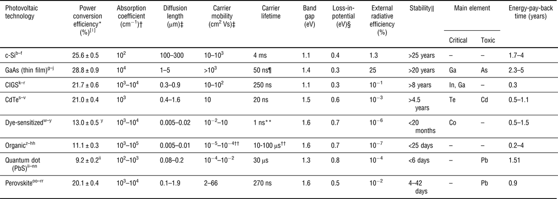

 Open access

