Introduction
For the past few decades, physical scaling of the device and gate dielectric have been the approach to enhance transistor performance.Reference Moore1 However, traditional silicon dioxide dielectrics have been pushed to the physical limit as the gate oxides are required to scale <1 nm (~3 atomic layers) for transistors having channel lengths below 45 nm. Hafnium-based high-κ dielectrics (HfO2 and HfSiOx), with a bandgap of ~5.7 eV, are the preferred material system due to their thermal stability with the Si substrate; they also have an appropriate κ value of ~16–25 (Reference 2) to achieve the relatively high capacitance with appropriate physical thickness.Reference Wilk, Wallace and Anthony3 The complementary metal oxide semiconductor (CMOS) device is based on the combination of nMOSFET (with electrons as the majority carrier) and pMOSFET (holes). Typical construction of the contact electrode for the two types of devices is differentiated by doping the polysilicon (poly-Si) electrode with n- and p-type dopants. This modulates the poly-Si effective work function (EWF) at ~4.0 eV and ~5.1 eV (for n- and p-type dopants, respectively), and enables a low threshold voltage (V t) for turning on a transistor.
V t is determined by the flatband voltage (V fb) across the device interface, and V fb is determined by the work function of the metal gate and the silicon substrate.

where φF is the surface potential in the silicon, and V ox is the potential in the gate dielectric. Furthermore,

where ΦMS is the work function difference between gate (ΦM) and substrate (ΦS); Q f is fixed oxide-silicon interface charge density; εox is dielectric constant of the insulator; and EOT is equivalent oxide thickness.
Integration of the high-κ dielectrics into the existing process flow with a poly-Si electrode has encountered key roadblocks involving interaction between the poly-Si and the high-κ material. The Fermi-level pinning phenomenonReference Hobbs, Fonseca, Dhandapani, Samavedam, Taylor, Grant, Dip and Triyoso4, Reference Yeo, Ranade, King and Hu5 suggests the Fermi level of the poly-Si is easily pinned to the energy level of the metal oxide surface states due to charge exchange between the electrode and the dielectric, therefore pinning the EWF of the electrode. The inability to modulate the EWF of the electrode by dopant changes results in an unfavorable increase in the threshold voltage (V t) for MOSFET devices to turn on (for nMOS, V tn increases ~0.4 eV; for pMOS, V tp increases ~0.7eV).Reference Yeo, Ranade, King and Hu5 The variables V tn and V tp refer to the threshold voltages for n- and p-type MOSFET devices, respectively. Another limitation to the use of poly-Si gates is the poly depletion effect while the MOSFET is turned on. This thin dopant depleted layer formed in the poly-Si adds to the EOT (~0.3 nm), which reduces the drain current and cannot be overlooked in technologies targeting <1 nm EOT.Reference Wong6 These scaling challenges have led to the choice of using metal gate electrodes to replace poly-Si gates.Reference Hu, Yang, Kraft, Rotondaro, Hattangady, Lee, Chapman, Chao, Chatterjee, Hanratty, Rodder and Chen7
An early paper from 1997 discussed the need for metal gates in future-generation scaled CMOS devices.Reference Hu, Yang, Kraft, Rotondaro, Hattangady, Lee, Chapman, Chao, Chatterjee, Hanratty, Rodder and Chen7 However, the choice of the appropriate electrode material has not been a trivial task, and the industry has only recently converged on the material and integration strategy.Reference Chudzik, Doris, Mo, Sleight and Cartier8–Reference Jan13 Details will be discussed more in the process integration section of this article. The primary reasons for this lack of consensus is that although EWF should be predominantly determined by the bulk/vacuum work function of the materials (materials in columns IIIB, IVB, and VB of the periodic table are suitable for n-type EWF; materials in column VIII have p-type EWFs),Reference Michaelson14 the determination of EWF of a metal gate on high-κ dielectrics exhibits a higher level of complexity, especially the understanding of factors controlling the EWF.
Standardized method for effective work function extraction
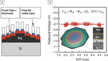
The terraced oxide method was proposed to enable the linear extraction of the EWF on high-κ materials from the V fb–EOT relationshipReference Wen15, Reference Brown16 and to avoid large errors in extracting the EWF from bulk charges in the high-κ material. Figure 1 shows the terraced oxide methodology, where on a single device wafer, the SiO2 dielectric is thermally grown (10 nm) and etched into ringed terraces of various thicknesses. Details of this process can be found in References 15 and 16. For EWF extraction on high-κ materials, a thin high-κ film (~2–3 nm) is deposited on the terraced oxide wafers, followed by metal electrode deposition. The terraced oxide method follows a three charge model (considering the fixed interface charge of the Si/SiO2 interface, the SiO2/high-κ interface, and minimized high-κ bulk charges) to enable linear V FB–EOT extraction, see reference 16 for more details of the extraction.Reference Brown16
Effective work function (EWF) extraction methodology used to evaluate hundreds of metal gates (see collective data in Figure 2 of the introductory article of this issue). (a) A schematic of the stack showing a fixed high-κ dielectric material on a varying interfacial SiO2 layer. (b) A flatband voltage versus equivalent oxide thickness curve used to extract the EWF from the y-intercept and fixed charges in the stack from the slope. The colored bands on the wafer are regions of different SiO2 thickness (oxide thicknesses in this image are extremely thick and for visual demonstration only; actual device SiO2 thicknesses can vary from 10 to 100 Å). The transmission electron microscopy inset shows a schematic cross-section of the typical device.

With the use of terraced oxide structures, a constant fixed interface charge density Q f is maintained across the varying oxide thicknesses. The extracted y-axis ordinate intercept value is used to extract the metal work function, and the slope is used to extract the fixed charges.
EWF control through metal gate material selection
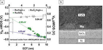
The effective work function of the metal electrodes can be modulated by changing the material composition (ΦM term). Pure metals and metal alloys have been demonstrated to exhibit a near linear relationship, with a work function range consistent with bulk work function values.Reference Wen17, Reference Wen18 However, interface stability of the pure metals with dielectrics is a concern due to additional thermal budgets arising from post gate stack processing. An extreme example of an interfacial reaction dominating the EWF is shown in Figure 2. Although Ru on SiO2 has a high EWF of 4.98 eV, the EWF of Ru on HfO2 is only 4.53 eV. Careful examination of the Ru/SiO2 interface shows an interfacial reaction of RuOx formation, while the interface stability of Ru on Hf-rich high-κ dielectric material is reasonable.Reference Wen, Lysaght, Alshareef, Huffman, Harris, Choi, Senzaki, Luan, Majhi, Lee, Campin, Foran, Lian and Kwong19 Intentional deposition of RuO2 on a high-κ material shows a high EWF—5.04 eV, confirming that the RuOx-like interface is the source of the high EWF on SiO2.
(a) Flatband voltage (V fb) versus equivalent oxide thickness (EOT) from terraced oxide wafers to extract the effective work function of Ru and RuO2 on SiO2 and on a high-κ material. (b) High-resolution transmission electron microscopy image of a Ru/SiO2 interface after a high temperature process showing an interfacial reaction region.

Therefore, the addition of constituents to stabilize the electrode material and provide improved thermal stability with the dielectric is needed. Certain additives to the metal, in particular nitrogen (metal nitrides)Reference Wen, Choi, Lysaght, Majhi, Alshareef, Huffman, Harris, Luan, Lee and Yamada20 and/or Si, Al (metal silicides,Reference Sim21 ternary metal-Si-N,Reference Wen22 metal-Al-NReference Wen23), have been evaluated and are proposed as possible improvements over pure metals as dual metal electrodes.
An extensive and systematic study of metal EWFs has been reported,Reference Wen24, Reference Alshareef25 where the range of EWF tunability for thermally stable metal electrodes is found to be limited to ~4.2–4.9 eV (see Figure 2 in the introductory article of this issue). The interface between the metal gate and high-κ dielectric is found to be critical in determining the EWF, and recent research focus has changed to utilizing interface control for EWF modulation.
EWF control through interface modulation
One such technique is via insertion of a dielectric capping layer between the metal/high-κ dielectric. For engineering toward p-type EWF, an Al-based top interface layer (TIL), such as Al2O3, or AlN of ~1 nm has been proposed.Reference Alshareef, Luan, Choi, Harris, Wen, Quevedo-Lopez, Majhi and Lee26 The EWF values of metal electrodes with Al-TIL increased by ~0.25 eV over their initial values, independent of the metal electrode system. Engineering the interface toward n-type EWF is also consistently demonstrated with the use of lanthanide-based dielectrics (La2O3, Y2O3). The effect is theorized to be due to the formation of a dipole layer at the high-κ/SiOx interface.Reference Kirsch27
Other techniques include interface modulation by diffusion of additional species (such as Al, La) to the metal/high-κ interface; this utilizes lessons learned from alloyed metals, but can only be implemented in the gate last flow, where the thermal stability requirement is less stringent. Details of this will be discussed in the process integration section of this article. EWF reduction and low V t NMOS transistors have been reported with the use of a low work function Al cladding layer.Reference Hinkle28
Reports of oxygen control at the metal/high-κ interface have been published, suggesting that an increased oxygen level at the interface can modulate the EWF toward PMOS needs.Reference Song29 One hypothesis proposed the cause to be a reduction of oxygen vacancies in the dielectric,Reference Song29 but recent reports suggest the increased oxygen level at the interface may be due to the displacement of N in nitride electrodes with O, thus forming an N-induced dipole at the TiN/HfO2 interface.Reference Hinkle, Galatage, Chapman, Vogel, Alshareef, Freeman, Wimmer, Niimi, Li-Fatou, Shaw and Chambers30
V fb or V t roll-off at low equivalent oxide thickness
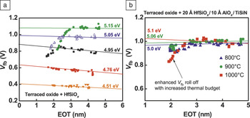
One of the most challenging issues in metal gate development is a gradual reduction (“roll-off”) in the V fb as the gate stacks are scaled to lower thicknesses for p-type electrodes. The onset of “roll-off” occurs at an EOT of ~2 nm (Figure 3a). The magnitude of roll-off (ΔV fb) is found to be enhanced with higher EWF (p-type) metals and with the increased thermal budget of the gate stacks. One theory of roll-off is its association with the generation of positively charged oxygen vacancies in the interfacial SiOx layer as oxygen diffuses out into the overlaying high-κ dielectric (Figure 3b).Reference Bersuker, Park, Wen, Choi, Sharia and Demkov31 The roll-off effect in transistors prevents V t scaling as EOT declines.
(a) Plot of V fb versus equivalent oxide thickness for high and low effective work function (EWF) metals showing gradual V fb reduction for high EWF metals. (b) V fb roll-off as a function of processing temperature.

Process integration of metal gate electrodes
The industry is divided between both gate-first Reference Chudzik, Doris, Mo, Sleight and Cartier8–Reference Arnaud10 and gate-lastReference Mistry11–Reference Jan13 high-κ/metal gate integration at the 45 nm and 32 nm device technology nodes. The gate-first integration scheme is characterized by deposition of the high-κ/metal gate stack at the start of the process. This deposition occurs at the same time as the standard polysilicon integration in the currently used process; the high-κ/metal gate stack simply replaces the SiO2/polysilicon. The high-κ/metal gate stack is then processed through the high temperature (> ~1000°C) of the source and drain activation anneal. On the other hand, the metal electrode in a gate-last integration scheme is deposited at a much later point in the process flow (typically following silicidation of the source and drain), and hence it is only exposed to the low thermal budget (< ~500°C) of the back-end process.
Gate-first flow
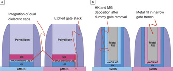
Figure 4a depicts cross-sections for typical gate-first integrated devices. The salient features are the dielectric capping layers specifically engineered to create favorable dipoles for setting the EWFs. The metal nitride electrode provides for high carrier densities to eliminate polysilicon depletion effects. The first challenge in a gate-first flow is integration of the dual dielectric capping layers. The first dielectric capping layer (typically Al2O3 for the PMOS device) is deposited across the entire wafer. Then the Al2O3 is selectively removed from the NMOS regions via a photolithography step and a wet etch step that is selective to the underlying HfO2 gate dielectric. Next, the NMOS capping layer (typically La2O3) is deposited and similarly patterned and wet-etched from the PMOS regions.Reference Tatsumura32 The metal nitride gate electrode and polysilicon top electrode are deposited, and the entire gate stack must be patterned to define the active gates. The next critical step occurs during the junction activation, which exceeds temperatures of 1000°C. This anneal not only diffuses and activates dopants in the junctions, but provides the thermal budget to trigger the EWF setting of the dielectric capping layers. However, this step also requires a balance between these beneficial mechanisms and the diffusion of metal from the capping layers to the dielectrics/semiconductor interface, which would cause deleterious V t shifts and mobility degradation.Reference Tatsumura32 The rest of the gate-first flow follows the conventional CMOS flow.
(a) Cartoon depicting a cross-section of typical gate-first integrated nMOS and pMOS devices. Only the gate stack and sidewall are shown for simplicity. The integration of dual dielectric caps and etch of the gate stack are key challenges of the gate-first approach. (b) Cartoon depicting a cross-section of typical gate-last integrated nMOS and pMOS devices. Removal of the dummy gate and metal fill in the narrow gate trench opening are key challenges of the gate-last approach. MG, metal gate; HK, high-κ dielectric.

Gate-last flow
The main feature of a gate-last flow is deposition of the high-κ/metal gate stack late in the flow benefiting from the low temperature thermal budget of the back-end processes. Some of the key challenges for gate-last integration are illustrated in Figure 4b. The salient feature of the gate-last process is the presence of high-κ dielectric and metal gate electrode films deposited alongside the interior walls of the spacer. This requires the removal of a dummy gate electrode (typically polysilicon) prior to the high-κ/metal gate stack deposition. The removal of the dummy polysilicon is challenging, requiring chemical-mechanical polishing to expose the dummy gatesReference Mistry11 and selective removal (a wet etch process utilizing NH4OH) of the silicon dioxide underneath the dummy gate. An atomic layer deposition process for high-κ dielectric and the nMOS and pMOS metal electrodes deposition is needed to ensure highly conformal deposition at the bottom of the gate stack. The critical step at this point in the flow is the selective patterning of the opposite electrode material from its complementary gate, which requires challenging photolithography and etching of the metal gate from the narrow gate trench. The gate stack formation is completed with the deposition of the metal fill material (typically Al). A final planarization of the surface using chemical-mechanical polishing completes the device formation.Reference Mistry11
When contrasting the advantages and challenges of gate-first versus gate-last processes, the control of the EWF is the deciding factor. Since the gate-last flow only exposes the gate stack to the low thermal budget of the back end, the EWF can be set and controlled to the desired band-edge target. This is especially important for the pMOS device, which has typically been susceptible to work function roll-off at high thermal budget.Reference Alshareef25 EOT control is another important aspect, since the use of dielectric capping layers in the gate-first flow results in a larger electrical thickness (~2 Å) on pMOS than nMOS.Reference Arnaud10 This is not the case for the gate-last flow, where the same EOT can be achieved on both nMOS and pMOS structures. The gate-last scheme is becoming a favorite among many device manufacturers.
Summary
The optimal metal gate material should achieve band-edge work function for low MOSFET threshold voltage control, while maintaining thermal stability on the high-κ dielectric. The key to this finding is that although material selection is important, the critical factor to attaining band-edge work function is in the structure and composition control at the high-κ/metal gate interface. Convergence in the industry in recent years has shown that interface engineering is the approach for “gate-first” process integration strategies, while a new low thermal budget “gate-last” integration process has made high-κ/metal gate technology possible.