Introduction
Over the last decade, the market for transparent conducting films has experienced exponential growth due to the proliferation of LCD displays, touch screens, and thin-film solar cells. Today, the transparent conducting film is ubiquitous. Popular devices such as LCD TVs, computer screens, solar cells, GPS units, cell phones, tablet computers, and e-book readers are all dependent on it. To make a smartphone, tablet computer, or GPS function requires five layers of transparent conducting films: one layer for the back-plane transistors, two layers for switching liquid crystal orientation, and two layers for the touch screen. For a single material, this represents more layers than any other material used for these devices.
To date, LCDs are the largest application for transparent conducting films, and they are forecast to continue to grow for the foreseeable future. In 2010, about 362 million touch screen panels were shipped. An annual growth rate of 20% is expected through 2013 for the touch screen market. With the popularity of e-readers such as the Kindle increasing, demand for transparent conducting films for electrophoretic displays (EPDs) is forecast to grow 30-fold from 2008 to 2014.Reference Hecht, Hu and Irvin1 Most significantly, the market demand for transparent conducting films in green energy applications, including electrochromatic windows, electroluminescent light (EL) panels, organic light-emitting devices (OLEDs), and thin-film solar cells, is growing at a rapid pace.
Tin-doped indium oxide (ITO) as a transparent conducting film dominates all market segments, except thin-film solar cells, wherein fluorine-doped tin oxide (SnO2:F) and aluminum-doped zinc oxide (AZO) have made great inroads. According to the Information Network, “ITO commanded a transparent conducting film market share of 97.6% in 2010, the revenue for the target alone was $6.99 billion.” With market demand increasing and new applications emerging, ITO increasingly becomes problematic in several aspects. An ITO film contains ∼90% indium oxide (In2O3). The indium is produced mainly as a by-product of zinc mining. Its supply is limited. The most viable method for ITO deposition is vacuum sputtering. The process is expensive and problematic for substrates, such as polycarbonate (PC), which has a tendency to de-gas under vacuum. ITO film is brittle—easy to crack when it is subject to deformation—a serious issue for both manufacturing yield and lifetime for flexible devices. Additionally, the ITO surface is active when in contact with a corrosive or organic material, resulting in interface instability. Therefore, there is a great need for alternatives to ITO (e.g., conducting polymers). Several new technologies are emerging, including silver nanoparticles and nanowires, graphene, and carbon nanotubes (CNTs). This article focuses on CNT technology. For a broad perspective of the field, readers can refer to several recent review articles.Reference Hecht, Hu and Irvin1–Reference Granqvist4
The first publication on CNT transparent conducting films can be traced back to a 1998 U.S. patentReference Shibuta5 issued to Hyperion Catalysis International, a corporation that pioneered multi-walled carbon nanotube (MWNT) commercial production and applications in the 1980s, and Mitsubishi Materials Corp. The targeted application was static charge dissipation for overhead projector transparent films (OPTFs). Unfortunately, the OPTF market disappeared (power point projection killed OPTF) before the application got off the ground. MWNTs, especially catalytically vapor grown MWNTs, tend to be defective, which lowers their conductivity and, consequently, their performance as transparent conducting films. For this reason, the development of CNT transparent conducting films has been primarily carried out using SWNTs and recently double-walled carbon nanotubes (DWNTs). This article reviews recent progress in CNT transparent conducting films and discusses fundamental properties of CNTs important for the formation of a transparent conducting film, methods for CNT dispersion, specially CNT ink formulation, CNT transparent conducting film coating, properties of the CNT transparent conducting films, and issues remaining to be solved in order to make the CNT transparent conducting film a commercial viable alternative to ITO.
Carbon nanotubes for transparent conducting films
CNTs have been proven to be a unique material for transparent conducting films. Several properties, including atomic arrangement of individual CNTs, microstructure of CNTs, and optical and electrical properties, are important for CNT transparent conducting films.
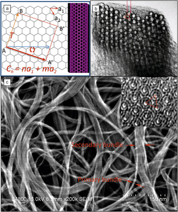
A single-walled carbon nanotube (SWNT) is a nano-cylinder comprised of a single layer of carbon atoms seamlessly bonded together by pyramidal sp 2 bonds. The atomic structure of a SWNT can be describedReference Dresselhaus, Dresselhaus and Eklund6, Reference Wilder, Venema, Rinzler, Smalley and Dekker7 (Figure 1a) by a chiral vector Ch:

(a) Schematic illustration of a single-walled carbon nanotube (SWNT) lattice: When a single layer of graphene defined by the area of ABA’, B’ is rolled up by connecting points A to A’ and B to B,’ a seamless SWNT (red) is formed. Its chiral vector and chiral angle are Ch = na 1 + ma 2 and  respectively. (b) High-resolution transmission electron microscopy (HRTEM) image of the end of a SWNT bundle; a triangular lattice (red) is evident. (c) Scanning electron microscopy image of a high purity and high conductivity double-walled carbon nanotube (DWNT) sample shows two levels of the structure—primary bundles with diameters from 3–10 nm and large secondary bundles. The primary bundle is crystallized with a triangular lattice (outlined in red in the inset). Inset: HRTEM image of the end of a DWNT bundle.

Here, n and m are a pair of integer indices, and a 1 and a 2 are the unit vectors. The two indices n and m define an angle from 0° to 30° between the chiral vector and the a 1 unit vector called the chiral angle. This structure affords SWNT unprecedented properties. Strong and seamless sp 2 carbon-carbon bonding determines the highest tensile modulus ever measured for a one-dimensional (1D) material, and the chiral angle and 1D confinement of electron and phonon states give rise to interesting optical and electronic properties. When n = m or (n – m)/3 = an integer, SWNTs are metallic. SWNTs with all other n and m combinations are semiconductors. Statistically, it has been estimated that about one-third of all SWNTs are metallic, and two-thirds are semiconducting. Of course, for transparent conducting film applications, one would like for all nanotubes to be metallic.
The micromorphology of CNTs is important for the preparation of CNT transparent conducting films. Highly crystallized SWNTs tend to form very tight bundles, called ropes. Thess et al.Reference Thess, Lee, Nikolaev, Dai, Petit, Robert, Xu, Lee, Kim, Rinzler, Colbert, Scuseria, Tomanek, Fischer and Smalley8 described these ropes to be comprised of 100–500 SWNTs all roughly parallel to each other arranged in a 2D triangular lattice (Figure 1b). The fundamental force inducing bundle formation is the van der Waals interaction. The strength of the force is dependent on the distance and relative orientation between tubes. Under extreme cases of aligned (i.e., crystalline bundle) and crossed, the attractive potentials have been deducedReference Coleman9, Reference Israelachvili10 as


where A is the Hamaker constant, D is the distance between CNTs, and R is the CNT radius. The attractive force is the strongest if CNTs are aligned to form crystalline bundles. Therefore, it is very difficult to separate CNTs from crystalline bundles, especially for long bundles, which is a critical step in the process of preparing CNT transparent conducting films. In addition to SWNTs, DWNTs have been proven that can be made into high purity and high conductivity.Reference Yoshida, Sugai and Shinohara11, Reference Niu12 Similar to high-quality SWNTs, DWNTs also form crystalline bundles (Figure 1c) with a 2D triangular lattice (inset in Figure 1c). Such crystalline bundles, with diameters from 3–10 nm (primary bundle), further agglomerate to form large secondary bundles. As can be seen in Figure 1c, the arrangement of the primary crystalline bundles in these large secondary structures is irregular, and loose points are evident; therefore, it is relatively easy to separate them.
Several methods have been developed for making CNTs, including dc arcReference Iijima and Ichihashi13, Reference Bethune, Kiang, Sde Vries, Gorman, Savoy, Vazquez and Bayers14 and laser vaporizationReference Guo, Nikolaev, Thess, Colbert and Smalley15 of graphite rod spiced with transition metals, and catalytic conversion of CO and hydrocarbons by an aerosol processReference Nikolaev, Bronikowski, Bradley, Rohmund, Colbert, Smith and Smalley16, Reference Howard, McKinnon, Makarovsky, LaFleur and Johnson17 and by a supported transition metal catalyst.Reference Hafner, Bronikowski, Azamian, Nikolaev, Rinzler, Colbert, Smith and Smalley18, Reference Qi, Qian and Liu19 The last, supported metal catalyst method is more suitable for commercial scale up. As produced, CNTs contain non-tube carbon impurities and catalyst residue. To use them for transparent conducting films, they need to go through a rigorous purification process, including a controlled oxidation step to remove unwanted carbon impurities and also defective CNTs, followed by an acid washing step to reduce catalyst residue to an acceptable level. Because the SWNT consists of only a single layer of carbon atoms, its oxidative stability is not much better than non-tube carbon impurities, therefore it is very difficult to control the oxidation condition to produce high purity SWNTs with high yield. With two layers of carbon atoms, the oxidative stability of DWNTs is ∼150°C higher than that of SWNTs.Reference Niu12 This makes the oxidation purification step of DWNTs relatively easy to control. Additionally, DWNTs are more metallic due to larger diameters and interaction between inner and outer tubes, which could turn certain tubes with a semiconducting-semiconducting combination into metallic tubes.Reference Zolyomi, Rusznyak, Kurti, Gali, Simon, Kuzmany, Szabados and Surjan20 Therefore, DWNT is a better candidate than SWNT for use to commercialize CNT transparent conducting films.
Carbon nanotube transparent film deposition
Most reports on CNT transparent film deposition have followed the solution route, except in a few casesReference Zhang, Fang, Zakhidov, Lee, Aliev, Williams, Atkinson and Baughman21–Reference Jiang, Li and Fan23 where transparent CNT films were prepared by directly drawing from super-aligned CNT arrays. In general, the solution approach uses a two-step strategy, first reportedReference Niu, Sichel, Hoch, Moy and Tennent24 in 1997, of disassembling CNTs in a liquid medium, and then assembling them into a network structure with random orientation.
To disperse and stabilize CNTs in a liquid involves overcoming and shielding the van der Waals interaction between CNTs by careful design and manipulation of a CNT-solution interface. Strategies employed include introduction of functional groups on the CNT surface,Reference Fu and Sun25 selection and design of organic solvents,Reference Ham, Choi and Chung26 and using surfactants and dispersants by leveraging the knowledge of colloid chemistry.Reference Niu, Sichel, Hoch, Moy and Tennent24, Reference Liu, Casavant, Cox, Walters, Boul, Lu, Rimberg, Smith, Colbert and Smalley27 A mechanical method, such as high shear rotor stator mixing or ultrasonication, is usually used to aid in disassembling the CNT agglomerates and aggregates in the preparation stage.
Surface functionalization has proven very effective for the solubilization of CNTs;Reference Fu and Sun25, Reference Ausman, Piner, Lourie, Ruoff and Korobov28 unfortunately, the formation of covalent bonding on the side walls of CNTs disrupts the conjugated sp 2 structure and reduces the conductivity. Therefore, the method is not suitable as a step for the preparation of high-performance CNT transparent conducting films. Direct solubilization of CNTs in an environmentally benign, low boiling point and low surface tension solvent without the addition of dispersion aids is ideal for CNT transparent film deposition. Many solvents have been investigated.Reference Ham, Choi and Chung26, Reference Bahr, Mickelson, Bronikowski, Smalley and Tour29, Reference Landi, Ruf, Worman and Raffaelle30 Based on data from previous studies, it is generally agreed that N-Methyl-2-pyrriolidone (NMP) and N,N-dimethylformamide (DMF) and their derivatives are the best. In a recent publication, Bergin et al.Reference Bergin, Sun, Streich, Hamilton and Colman31 claimed the preparation of high concentration SWNT dispersion up to 3.5 mg/cc using cyclohexyl-pyrrolidone as a solvent. But, to date, no report has shown that high-quality CNT transparent conducting films can be prepared from these solvent dispersions. Both NMP and DMF are toxic, especially DMF, which has been linked to cancer. So, the search for a CNT solvent continues.
The third approach—dispersing CNTs in water aided by a surfactant or dispersant—is very promising. All types of surfactants, including anionic, cationic, non-ionic, and zwitterionic,Reference Liu, Casavant, Cox, Walters, Boul, Lu, Rimberg, Smith, Colbert and Smalley27, Reference Moore, Strano, Haroz, Hauge, Smalley, Schmidt and Talmon32–Reference Tan and Resasco34 plus various dispersants, have been investigated. Ionic surfactants, such as sodium dodecyl benzene sulfonate (SDBS), sodium diisopropyl naphthalene sulfonate (SDNS), and hexadecyltrimethyl ammonium bromide (CTAB), have proven most effective. A common feature of these ionic surfactants is their amphiphilicity, with a hydrophobic tail and a hydrophilic head group that is highly ionizable in water. A dispersion process is a dynamic CNT surface area exposing (increasing) process. When CNTs and a surfactant are added to water, the surfactant molecules are quickly adsorbed onto the CNT surface, which is accessible via its hydrophobic tail. A mechanical force, often ultrasonication, is applied to aid CNT separation and expose more CNT surface. Freshly exposed CNT surfaces are quickly covered up by the surfactant, resulting in smaller CNT bundles and individualized CNTs, with their surface charged either negatively or positively induced from the ionization of the surfactant head groups. Coulomb repulsion between them prevents re-aggregation and stabilizes the dispersion. The pH is important to maximize this repulsion.Reference Tan and Resasco34 Typically, the pH for a stable dispersion using an anionic surfactant is on the basic side and is on the acidic side for the system using a cationic surfactant.
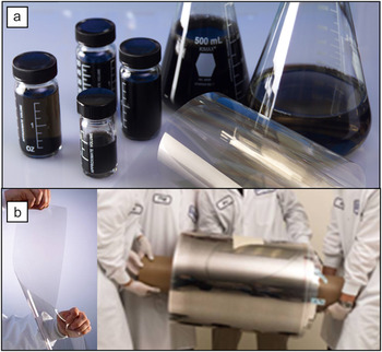
Most CNT-water dispersions reported in the literature are prepared using a single surfactant or dispersant, which is simple to study and sufficient for the preparation of small CNT transparent conducting film samples for investigation. Various methods, including vacuum filtration and transferring,Reference Wu, Chen, Du, Logan, Sippel, Nikolou, Kamaras, Renolds, Tanner, Hebard and Rinzler35, Reference Hu, Hecht and Grüner36 spin coating,Reference Meitl, Zhou, Gaur, Jeon, Usrey, Strano and Rogers37, Reference Jo, Jung, Lee and Jo38 electrophoretic deposition, followed by hot pressing transfer,Reference Pei, Du, Zheng, Liu and Cheng39 dip coating,Reference Spotnitz, Ryan and Stone40 casting,Reference Sreekumar, Liu, Kumar, Ericson, Hauge and Smalley41 spraying,Reference Haempgen, Duesberg and Roth42 and Mayer rod drawing,Reference Dan, Irvin and Pasquali43 have been used for the preparation of CNT films. Unfortunately, these simple CNT dispersions and most of these methods are not suitable for industrial scale up. A CNT ink product, robust enough for industrial film production, is more complex. In addition to CNTs, water, and surfactant, a proper CNT ink contains a list of ingredients in various levels, such as rheology modifiers for the control of viscosity, humectants for the regulation of drying characteristics, defoam or antifoam agents to minimize foaming, wetting agents to reduce surface tension and enhance the spreading on the substrate, adhesion promoters to enhance CNT adhesion to the substrate, and biocides to inhibit fungal and bacterial growth. To add to the complexity, most of these additives, including the primary surfactant, have to be removed after coating is formed in order to maximize the conductivity of the CNT layer. Figure 2 shows inks (Figure 2a) in glass containers formulated for roll-to-roll coating of CNT transparent conducting films on plastic substrates, and a roll of the CNT film (Figure 2b) produced by an industrial roll-to-roll coating method at high speed.
(a) Carbon nanotube (CNT) inks. (b) A piece of CNT transparent conducting film held in the air (left), and a roll of CNT transparent conducting film product (right).

Properties of CNT transparent conducting films
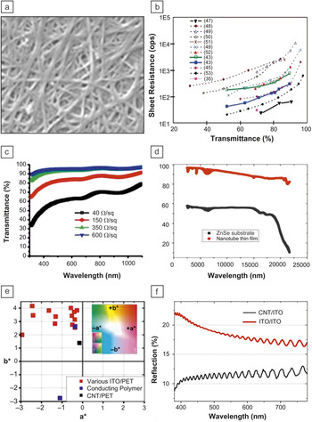
Figure 3a shows a typical scanning electron microscope (SEM) image of a CNT transparent conducting film, a porous network structure formed by randomly entangled CNT bundles. All bundles lay flat relative to the substrate surface. This structure determines the properties of CNT transparent conducting films. The two most important properties are the sheet resistance and optical transmittance to visible light. Both sheet resistance and transmittance are thickness dependent—decreasing as the thickness increases. For most applications, it is desirable to have high transmittance and low sheet resistance. For a specific application, a compromise between the two properties has to be made. The film thickness for a CNT transparent conducting film is typically less than 50 nm, which is significantly less than the wavelength of visible light. Hu et al.Reference Hu, Hecht and Gruner44 showed that in this range of the thickness, the model for thin metal films is applicable. The relation between transmittance (T) and sheet resistance (R s) can be described by the following equation:

Structural and optoelectronic properties of carbon nanotube (CNT) transparent conducting films: (a) scanning electron microscopy image of a CNT transparent conducting film—randomly entangled CNT bundle network. (b) Comparison of the electro-optical properties of CNT transparent conducting films reported in the literature.Reference Wu, Chen, Du, Logan, Sippel, Nikolou, Kamaras, Renolds, Tanner, Hebard and Rinzler35, Reference Dan, Irvin and Pasquali43, Reference Zhou, Hu and Gruner45, Reference Hecht, Heintz, Lee, Hu, Moore, Cucksey and Risser47–Reference Geng, Kim, So, Lee, Chang and Lee53 (c) Transmittance dependence on the wavelength from 300 nm to 1100 nm of four different single-walled carbon nanotube (SWNT) films. (d) Infrared transmittance of an SWNT film measured from a CNT film deposited on a ZnSe substrate. (e) Color coordinates of CNT, conducting polymer, and tin-doped indium oxide (ITO) films on poly(ethylene terephthalate) substrates. (f) Comparison of reflection spectra of CNT/ITO and ITO/ITO touch panels.

where, μ0 and ε0 are the free space permeability and permittivity, and σop and σdc are the optical conductivity and dc conductivity, respectively. It has been found that σop = ∼200 S/cm at 550 nm,Reference Zhou, Hu and Gruner45, Reference Buzicka, Degiorgi, Gaal, Thien-Nga, Bacsa, Salvetat and Forro46 which is related to the CNT network density, is not strongly related to variables such as CNT-CNT junction, CNT length, and doping. This provides an easy way to estimate the dc conductivity from measured R s and T without measurement of the film thickness.
Electrons transported through a CNT network (Figure 3a) have to jump from bundle to bundle. The resistance within the CNT bundle is significantly lower than the contact resistance between bundles, so the contact resistance is dominant. Figure 3b compares the sheet resistance and transmittance of CNT films reported by several groups.Reference Wu, Chen, Du, Logan, Sippel, Nikolou, Kamaras, Renolds, Tanner, Hebard and Rinzler35, Reference Dan, Irvin and Pasquali43, Reference Hecht, Heintz, Lee, Hu, Moore, Cucksey and Risser47–Reference Geng, Kim, So, Lee, Chang and Lee53 The performance of the films is strongly sample history and thickness dependent (Figure 3c). Acid treatment has been used as a means to improve performance, which reduces contact resistance by removing the surfactant used for CNT dispersion and also dopes the CNT by protonating it. Doping with a super acid or a strong electrophile is very effective for conductivity enhancementReference Jackson, Domercq, Jain, Kippelen and Graham54, Reference Kim, Jo, Kim, Duong, Shin, Han, Choi, Kong and Lee55 because about two-thirds of CNTs are semiconducting. Hecht et al.Reference Hecht, Heintz, Lee, Hu, Moore, Cucksey and Risser47 prepared CNT transparent conducting film using a chlorosulfonic acid dispersion of Unidym’s OE-grade CNTs and measured a sheet resistance of 60 Ω/sq at a transmittance of 90.9%, which corresponds to a dc conductivity of 12825 S/cm. This is the highest dc conductivity reported for a CNT film and matches the performance of ITO films on plastic substrates. Unfortunately, the stability of this dopant effect remains an issue, and furthermore, acidic dopants could be troublesome for applications requiring direct contact of the CNT film with active materials. Since the resistance of CNT films is dominated by contact resistance between CNT bundles, it is desirable to have longer tubes in the film. Hecht at al.Reference Hecht, Hu and Gruner56 showed that the conductivity of SWNT networks depends on the average SWNT length as a power law, σ ≈ Lav 1.46 and also on the CNT bundle diameter, σ ≈ Dav –β (β is between 0 and 2). Therefore, longer CNTs and better dispersions (smaller bundles) will lead to higher conductivity CNT films.
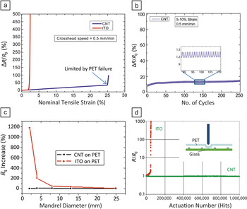
Several properties are unique to CNT transparent conducting films. Hu et al.Reference Hu, Hecht and Gruner57 showed that the CNT film is transparent in the infrared up to a wavelength of 20 μm (Figure 3d). The high plasma cut-off edge is due to the fact that CNT is a low charge carrier density but very high mobility conductor. Figure 3e compares color coordinates of CNT films (black) with those of a conducting polymer (blue) and several commercial ITO films (red). The transmittance of the CNT film is less wavelength dependent (Figure 3c), resulting in a near neutral color. ITO is yellowish, and the conducting polymer is bluish. The neutral color is highly desirable for most applications. The index of refraction of CNT is ∼1.5–1.6, which is closer to glass (1.5) and poly(ethylene terephthalate) (PET) (1.57), a widely used commercial substrate for transparent conducting films, than ITO (∼2.0); therefore, the reflection from CNT films is significantly less than ITO films (Figure 3f). Due to the unique network structure formed by random entanglement of CNT bundles, CNT films have unprecedented mechanical properties.Reference Sierros, Hecht, Banerjee, Morris, Hu, Irvin, Lee and Cairns58 Figure 4a compares relative sheet resistance change of a CNT film to an ITO film under uniaxial tensile strain. The ITO film fails at ∼2.5%, while the sheet resistance of the CNT film slightly increased as the strain increased up to ∼25%, at which point the PET substrate failed. Under repeated strain cycles from 5% to 10%, the sheet resistance of the CNT film remained relatively flat after an initial 10% increase (Figure 4b). A standard mandrel bending test (Figure 4c) showed that the sheet resistance of a CNT film remained unchanged after being wrapped around a 2 mm diameter mandrel, while the ITO film started to crack at 8 mm. Figure 4d compares standard pen hitting durability results of two touch panels, one with CNT/PET and ITO/glass electrodes, and the other with ITO/PET and ITO/glass. The all ITO panel failed after ∼60,000 hits, and the CNT panel had no change up to 1,000,000 hits. Furthermore, because the CNT surface is chemically inert and stable under corrosive conditions, CNT transparent conducting films are corrosive resistant.
Mechanical properties of carbon nanotube (CNT) transparent conducting films: (a) comparison of relative sheet resistance of CNT/poly(ethylene terephthalate) (PET) film with tin-doped indium oxide (ITO)/PET film under uniaxial tensile strain. (b) Strain cycle results from 5% to 10%. (c) Mandrel bending stability comparison of CNT/PET and ITO/PET. (d) Hitting pen durability comparison of CNT/ITO and ITO/ITO touch panels. Inset: Schematic view of testing apparatus, pen tip radius: 0.8 mm, load: 250 g.

Applications
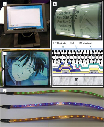
The straightforward application for CNT transparent conducting films is direct replacement of ITO, which has been the focus of most of the studies.Reference Hecht, Thomas, Ladous, Lam, Park, Irvin and Drzaic59–Reference Contreras, Barnes, van de Lagemaat, Rumbles, Coutts, Weeks, Glatkowski and Peltola61 The performance of CNT films is becoming increasingly competitive with ITO for applications, such as resistive touch screen sensors,Reference Hecht, Thomas, Ladous, Lam, Park, Irvin and Drzaic59 flexible LCDs,Reference Schindler, Schau and Fruehauf60 EPDs, and flexible LED strips. The CNT film is at the market entry stage for these applications. Figure 5 shows a fully functional 10.1” resistive touch screen (5a), a 14.3” flexible color EPD device (5b), and three flexible color LED strips (5d) fabricated using a CNT film as the top electrode. For EPD devices, high sheet resistance up to 10 kΩ/sq can be tolerated. The feasibility of using CNT films as pixel switch electrodes, which change the orientation of liquid crystals (Figure 5c), for LCD displays,Reference Schindler, Schau and Fruehauf60 window electrodes for inorganic thin-film solar cells,Reference Contreras, Barnes, van de Lagemaat, Rumbles, Coutts, Weeks, Glatkowski and Peltola61 and electrodes for projected capacitive touch screen sensors have also been demonstrated. But in order to be competitive in these markets, significant improvement in the performance of the CNT films is still needed.
(a) Resistive touch screen (10.1”) fabricated using a carbon nanotube (CNT)/poly(ethylene naphthalate) (PEN) film as the window electrode. (b) Flexible color electrophoretic display (14.3”) fabricated using a CNT/PEN film as the top transparent electrode. Bottom: Cross section view of the pixel, (c) 5.5” VGA full color LCD display fabricated using a CNT film as both common (on color filter) and pixel switch (on thin-film transistors) electrodes. (d) Flexible LED strips (10”) using a CNT/PET film as the transparent top lead.

As discussed in the previous section, there are several properties unique to CNT films, which make CNT films more suitable for organic semiconductor devicesReference Aquirre, Auvray, Pigeon, Izquierdo, Desjardins and Martel62–Reference Barnes, Bergeson, Tenent, Larson, Teeter, Jones, Blackburn and van de Lagemaat64 in spite of higher sheet resistance compared to ITO, especially when the device durability is included in the consideration. The surface of CNT films is porous and much more chemically compatible with organic semiconductors, which could lead to high contact area and a high-quality interface, which is important for performance enhancement; contrary to most oxide transparent conducting materials, a CNT film is a natural p-type conductor with a relatively high work function of 4.5–5.1 eV, eliminating the reverse voltage barrier when used as the anode to replace n-type ITO; additionally, a CNT film is stable when in contact with corrosive poly(3,4-ethylenedioxythiophene) poly(styrenesulfonate) (PEDOT/PSS). Note that PEDOT/PSS would corrode ITO and cause indium to diffuse into the active layers, resulting in device degradation. Several groups reported excellent device performance using CNT films as the anode for OLEDs and organic photovoltaics (OPV). Most significantly, Barnes et al.Reference Barnes, Bergeson, Tenent, Larson, Teeter, Jones, Blackburn and van de Lagemaat64 demonstrated that a CNT film promotes hole transport when used as an anode in organic solar cells and has the potential to replace both ITO electrode and the hole transport layer. Despite the relatively high sheet resistance and low transmittance of the CNT film, they were able to fabricate an organic solar cell without the hole transport layer exhibiting an NREL-certified efficiency of 2.65% and a short circuit current density of 11.2 mA/cm2, comparable to the performance of an ITO device with a hole transport layer.
Future perspectives
In the past several years, great progress has been made in (CNT) transparent conducting films. The performance of CNT films is now comparable to that of tin-doped indium oxide (ITO) films supplied for the resistive touch screen market. CNT film has been produced successfully using high-speed industrial roll-to-roll processes with water-borne CNT inks, and the cost of CNT film is projected to be competitive with ITO even at current high CNT prices because of the low-cost solution coating method and the minute amounts of CNT required to make a large area conducting. CNT film is poised for entry into the resistive touch screen, flexible electrophoresis display (EPD) and flexible LED markets. Due to its unique surface chemistry, p-type conductivity, and robust network structure, CNT film has great potential for use as the anode for OLED and OPV, electrodes for emerging devices such as curved or 3D touch sensors, and electrodes for roll-to-roll flexible electronics manufacturing. Furthermore, a CNT film is also infrared (IR) transparent, opening doors for exploring highly efficient solar cells by converting more solar spectra into electricity, IR radiation cooling, and new applications requiring both conducting and IR transmission.
Although performance remains the major barrier for CNT films to replace ITO in the broad market, the prospect for improvement is great in every step of CNT film preparation, from CNT growth, CNT dispersion, and to CNT coating. The most important area to explore is chiral selective growth of metallic CNTs. Increasing the percentage of metallic CNT concentration in CNT film could lead to transparent conducting films with a performance better than that of ITO. Significant improvement also could be achieved by developing new dopants that are stable, new surfactants and better dispersion processes for stable CNT inks with a high level of CNT dispersion, and methods for CNT-CNT junction resistance reduction. With further performance improvement, CNT transparent conducting films could become the second successful CNT commercial product after multi-wall carbon nanotube conducting plastic composites. More importantly, unlike ITO, the supply will be endless, because CNTs can be manufactured using renewable resources, such as CO and alcohol.