Introduction
Flexible electronics enable the development of displays, photovoltaics, radio-frequency identification (RFID) tags, and sensors that can be applied in challenging and novel environments or created at low-cost.[ Reference Crone, Dodabalapur, Lin, Filas, Bao, LaDuca, Sarpeshkar, Katz and Li 1 – Reference Jeong and Moon 5 ] High-throughput, cost-effective large-area processing is critical in expanding the application of these technologies, with solution processing being viewed as particularly facile. Oxide electronic materials, including both crystalline oxide and amorphous ternary and quaternary complex oxides, can provide useful electrical properties, high chemical and thermal stability, and high transparency while employing relatively common and nontoxic elements.[ Reference Hosono 6 , Reference Exarhos and Zhou 7 ] In addition, oxide materials with high dielectric constant and wide band gap are widely used as gate dielectrics in low-voltage field-effect transistors (FETs), though many of these are formed at high temperatures.[ Reference Robertson 8 , Reference Robertson 9 ]
In flexible electronics applications employing a polymer substrate, low processing temperatures (<300 °C) are required to avoid thermal degradation or distortion of the substrate, as electron-rich functional groups oxidize and most polymers are well above their glass transition temperatures at 300 °C. It is a challenge to fabricate a dense impurity-free oxide semiconductor film below that temperature.[ Reference Fortunato, Barquinha and Martins 10 , Reference Thomas, Pattanasattayavong and Anthopoulos 11 ] To reduce precursor decomposition temperature, water-based zinc oxide (ZnO) precursors have been synthesized.[ Reference Meyers, Anderson, Hung, Thompson, Wager and Keszler 12 – Reference Lin, Faber, Zhao, Wang, Amassian, McLachlan and Anthopoulos 15 ]
A second approach to low-temperature solidification of oxide thin films harnesses the rapid release of energy during a localized exothermic redox reaction ignited by a low annealing temperature.[ Reference Kim, Kanatzidis, Facchetti and Marks 16 , Reference Hennek, Smith, Yan, Kim, Zhao, Dravid, Facchetti and Marks 17 ] The reaction is generated by incorporating components acting as oxidizer and fuel into the precursors. Acetylacetone or urea is used as a “fuel” and metal nitrates serve as oxidizers. Recently, a polymer-dominated self-combustion aluminum oxide precursor [(3-glycidoxypropyl)trimethoxysilane (GPTMS) to aluminum molar ratio ≥8:1] was introduced to improve the combustion efficiency.[ Reference Bae, Kang, Han, Lee and Cho 18 ] With this precursor, a silane-AlO x composite gate dielectric film exhibited low leakage current after annealing at 250 °C, though tens of volts were required to turn on transistors made therewith.
It has remained challenging, however, to fabricate robust high-k oxide-based dielectric materials at low temperature with simple experimental settings without vacuum and/or external energy to assist film solidification.[ Reference Lin, Faber, Zhao, Wang, Amassian, McLachlan and Anthopoulos 15 , Reference Bae, Kang, Han, Lee and Cho 18 ] In our previous research, sol–gel solution-processed alkali metal ion-incorporated aluminas demonstrated very high capacitance with low leakage current and thus became a good candidate for low-voltage FETs.[ Reference Pal, Dhar, See and Katz 19 – Reference Liu, Guan, Zhang, Falk and Katz 21 ] In other previous work, to achieve high transistor performance in low-temperature-processed FETs, vacuum, and/or ultraviolet light irradiation has generally been required for the alumina dielectric annealing process.[ Reference Lin, Faber, Zhao, Wang, Amassian, McLachlan and Anthopoulos 15 , Reference Jo, Kim, Kim, Kang, Kim, Kim, Ko, Kim and Park 22 ] Here we demonstrate low-temperature-processed high-capacitance sodium-incorporated-alumina dielectrics based on two types of combustion precursors and compared their compatibility with aqueous solution-processed ZnO in FET applications.
In the first precursor, aluminum nitrate was used as the oxidizer and urea was used as fuel. A second self-combustion sodium-incorporated alumina (SA) precursor was also prepared using aluminum nitrate and aluminum acetylacetonate as oxidizer and fuel, respectively. GPTMS was added to the self-combustion precursor as a binding agent to cross-link the aluminum oxide matrix. In contrast to other types of silanes, blending GPTMS in SA precursor did not change the hydrophilic nature of the SA thin-film surface, and this could be related to the formation of polar functional groups as the epoxy groups open during curing. In some cases, the silane stabilized the SA film against etching during subsequent deposition steps, and the high dielectric constant of GPTMS was beneficial in maintaining the high capacitance of the SA dielectric. In the self-combustion precursor solution used in this study, the GPTMS to Al3+ molar ratios are 10:1 (10 at% GPTMS) and 2:1 (50 at% GPTMS). The high-concentration aqueous ZnO precursor deposited on the SA was prepared with a simplified method without precipitate formation and thus avoids time-consuming centrifugation, decantation, and evaporation steps required in previous reports.
Results and discussion
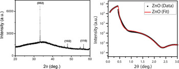
The crystallinity of low-temperature-processed ZnO thin film was probed using x-ray diffraction (XRD) following the creation of ZnO layers by spin-coating the aqueous ZnO precursor on a silicon dioxide SiO2/Si substrate and annealing at 200 °C. As shown in Fig. 1(a), the sharp (002) peak in the XRD pattern shows that the ZnO has the wurtzite crystal structure with preferred growth along the c-axis. A ZnO film made under identical conditions on a bare silicon wafer had a thickness of 6 ± 1 nm as characterized by x-ray reflectivity (XRR), as shown in Fig. 1(b).
(a) XRD pattern of ZnO thin film annealed at 200 °C for 1 h, acquired using Cu K α radiation with a wavelength of 1.5406 Å. (b) XRR of a ZnO film deposited on an Si wafer using identical conditions, also acquired with Cu K α radiation. The fit of an XRR model gives a ZnO layer thickness of 6 ± 1 nm.

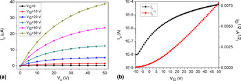
ZnO FETs were fabricated on Si substrates to evaluate the electrical properties of the ZnO layer. The aqueous ZnO precursor was spin-coated on a heavily n-type-doped Si substrate, with a 300 nm SiO2 layer to serve as a gate dielectric, and annealed at 200 °C in air. Figure 2 shows representative output and transfer characteristics of ZnO FETs fabricated using this process. The drain current demonstrates a good modulation behavior (on/off >10,000) induced by gate voltage. Based on an analysis of more than 30 FETs, the maximum saturation field-effect mobility was 0.7 cm2/V/s. A representative transfer curve is shown in Fig. 2(b), for which the on/off current ratio was 6.2 × 10⁴, the threshold voltage was 5 V, and the subthreshold slope was 5.7 V/decade.
(a) Output and (b) transfer characteristics of ZnO-based FETs with 300 nm SiO2 gate dielectric annealed at 200 °C for 1 h.

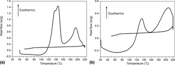
To realize low operation voltage in low-temperature-processed ZnO FETs, two types of SA combustion precursors were prepared and analyzed. Thermal analysis was carried out to analyze the redox exothermic reaction in the combustion SA precursors. Two exothermic reaction peaks at about 140 and 190 °C were observed in the urea-based SA precursor as shown in Fig. 3(a). This result corresponds to a two-step precursor conversion below 200 °C. The high-intensity exothermic peak at 140 °C could be caused by the reaction between aluminum nitrate nonahydrate and a more reduced compound, urea. The low-intensity exothermic peak at 190 °C could be attributed to a separate redox reaction between aluminum nitrate nonahydrate and aluminum acetylacetonate.
Differential scanning calorimetry (DSC) scan of (a) combustion SA precursor with urea; (b) self-combustion SA precursor with 50 at% GPTMS.

Similar to the urea-based combustion SA precursor, two exothermic reaction peaks at 135 and 200 °C were observed in the self-combustion precursor SA sample, shown in Fig. 3(b). The low-intensity exothermic peak at 135 °C could be related to the energy released from the ring opening reaction of GPTMS. The high-intensity exothermic peak observed at 200 °C would correspond to self-combustion reaction between aluminum nitrate nonahydrate and aluminum acetylacetonate.
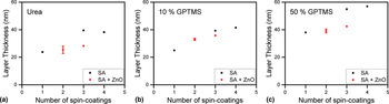
Thin films fabricated using SA compositions with urea, 10 at% GPTMS, and 50 at% GPTMS precursors were characterized using XRR to determine the thickness of the oxide layer deposited in each step. A final anneal at 500 °C was performed prior to the XRR analysis to eliminate any possibility of solvent contributions to the thicknesses. The initial spin-coating of the urea-based, 10 at% GPTMS, and 50 at% GPTMS materials gave layers that were 24, 25, and 38 nm thick, respectively. Figures 4(a)–4(c) show the dependence of the final layer thickness as a function of the number of spin coatings. Subsequent coatings yielded additional thickness, but not the same increments as from the first layer.
SA layer thickness measured using XRR as a function of the number of repetitions of the spin-coating process for (a) urea; (b) 10 at% GPTMS; and (c) 50 at% GPTMS precursors. The black dots are measurements from thin films consisting of the SA layer only. The thickness of the SA layer does not increase proportional to the number of spin coating steps. Red dots are the total thickness of samples in which the SA layer is capped by a ZnO layer. The application of the ZnO layer etches the underlying SA layer, while still forming the ZnO top layer. “Spins” refers to consecutive spincoating depositions of alumina precursor.

Figure 4 also includes the thicknesses of structures in which ZnO thin films were grown on top of the SA layers, as would be done for FETs. The ZnO layers were deposited using the process described above. The fabrication of the ZnO layer reduces the thickness of the SA film by approximately 10 nm, even as a ZnO layer is also formed. This etching effect will also be apparent in the discussion of the FET characteristics of the SA/ZnO layers discussed below. Compared with the urea combustion precursor-prepared SA film, the self-combustion precursor-prepared SA film with 10 at% GPTMS exhibited a smaller decrease in SA thickness after ZnO coating, suggesting a higher resistance to ZnO etching. A conspicuous increase in SA film thickness was obtained by increasing the amount of GPTMS from 10 to 50 at%, but this came with an apparent susceptibility of the GPTMS itself to being etched. The film roughnesses determined by XRR are consistent with those observed in the atomic force microscopy (AFM) studies shown in the supporting information.
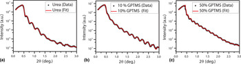
The XRR pattern of SA layers using two coating/annealing cycles and ZnO-coated on SA layers prepared in this way are shown in Fig. 5. Two independent oscillation frequencies are apparent in the reflectivity curves of the SA layers in Fig. 5 indicating that the SA layer has an inhomogeneous electron density along the surface normal direction. Annealing of SA films at 500 °C for 1 h thus creates a sublayer of different electron density. The average thickness of the sublayer within the SA layer is 5.3 ± 1.7 nm in all of the layers, approximately 10% of the total thickness.
XRR patterns of (a) ZnO on SA film prepared by the urea precursor; (b) ZnO on SA film prepared by precursor with 10 at% GPTMS; and (c) ZnO on SA film prepared by precursor with 50 at% GPTMS. In all samples, SA films were spin-coated twice. ZnO thin films grown on the SA layer were fabricated in a single round of deposition and annealing.

The interface roughnesses between ZnO and SA prepared by urea precursor, 10 at% GPTMS precursor, and 50 at% GPTMS precursor were measured using the XRR curves in Figs. 5(a)–5(c). The data are fit using the GenX software package, using the interdiff model.[ Reference Björck and Andersson 23 ] This model uses the fitting process to determine the thicknesses and electron density of the thin film's component layers as well as the root-mean-square (rms) roughness of the interface between the layers. The interfacial roughness can be interpreted as a graded region going from the electron density of one layer to the other. The SA/ZnO interface roughness of SA prepared by the urea precursor, 10 at% GPTMS precursor, and 50 at% GPTMS precursor are 1.35, 1.25, and 0.50 nm, respectively. SA layers prepared by precursors with GPTMS thus exhibited a smoother SA/ZnO interface than SA prepared with the urea precursor. The abruptness of the SA/ZnO interfaces increases with increasing GPTMS concentration.
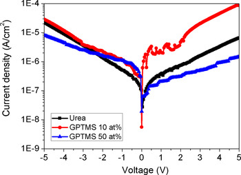
It is generally challenging to obtain low leakage current in solution-processed dielectrics annealed at low temperature.[ Reference Socratous, Banger, Vaynzof, Sadhanala, Brown, Sepe, Steiner and Sirringhaus 24 – Reference Huang, Duan, Dong, Zhang and Qiu 26 ] Incomplete decomposition of precursor solution and/or formation of pores during low-temperature annealing provide charge transport channels and/or breakdown sites, and lead to high leakage current. Leakage current could also be caused by pinholes, defects, and impurities in gate dielectric films, charge carrier tunneling due to the overlap of gate to source/drain electrodes, cross-talk between adjacent transistors, and unfavorable expansion of source/drain electrodes within the semiconductor layer.[ Reference Dickey, Subramanian, Anthony, Han, Chen and Loo 27 – Reference Ireland, Liu, Spalenka, Jaiswal, Fukumitsu, Oishi, Saito, Ryosuke, Evans and Katz 30 ] In this study, low leakage current was achieved in all SA metal–insulator–metal (MIM) capacitors between −5 and 5 V, shown in Fig. 6. The dielectric films were formed by spin-coating SA precursors twice, pre-baking on a hot plate at 75 °C for 15 min. The thickness of the SA dielectrics varies from 30 to 50 nm.
Leakage current of SA thin film prepared by urea-based combustion precursor and self-combustion precursor with 10 and 50 at% GPTMS.

The leakage currents of all SA samples were of the same order of magnitude as the leakage current of 500 °C-annealed SA MIM capacitors reported previously.[ Reference Keum, Bae, Kim, Choi and Lee 29 ] Self-combustion SA (50 at% GPTMS) MIM capacitors exhibited a lower leakage current than urea-based combustion precursor-processed SA capacitors. Supported by surface morphology data shown in the supporting information, this could be related to denser film structure in the self-combustion SA film with the incorporation of GPTMS. As expected, leakage current decreased significantly by increasing the GPTMS amount from 10 to 50 at%, especially in the positive voltage region. In thin-film capacitors, catastrophic dielectric breakdown was rarely observed. In our samples, the highest leakage current density of low-temperature-processed SA dielectric films is of the order of 1×10⁻³ A/cm2 with applied voltage between −10 and 10 V. Additional data are shown in Fig. S7. Based on the optimized current leakage and smoothness, SA films prepared with self-combustion precursor were chosen for the gate dielectric in ZnO-based FETs fabricated with a final annealing temperature of 250 °C.
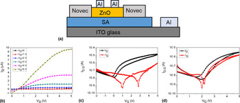
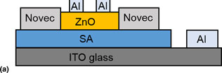
To further lower gate leakage current, the ZnO layer was patterned by a commercially available hydrophobic fluorinated polymer (Novec™) The schematic of FETs with ZnO semiconductor patterned using the fluorinated polymer is shown in Fig. 7(a). With a patterned ZnO layer, a small I D offset was obtained in transistor output characteristics. At a gate–source potential of 5 V, FET performance was achieved with a saturation field-effect mobility of 0.5 cm2/V/s, on/off current ratio of 1.0 × 10³, and subthreshold slope of 0.54 V/decade [Figs. 7(b)–7(d)]. Parameters including statistics for these and related devices are shown in Table 1 of the Supporting Information.
(a) Schematics of patterned ZnO-based FET configuration. (b) Output characteristics and (c) transfer characteristics of ZnO FETs with self-combustion precursor (50 at% GPTMS)-based SA gate dielectric. On/off ratio was 1000. The much higher leakage current in an unpatterned control is shown in (d).

Experimental
Low-temperature aqueous ZnO precursor was prepared by dissolving zinc nitrate hexahydrate (Sigma Aldrich) in ammonium hydroxide (Fisher) with a zinc concentration of 0.6 M. The concentration of ammonium hydroxide used for ZnO is 28.0–30.0 wt.% (14.8% N).
Acetylacetone (0.2 M) (Sigma Aldrich) was added as stabilizer. After stirring at room temperature for 30 h, the precursor solution was filtered through a 0.45-μm polyvinylidene difluoride filter and then diluted with ultrapure water (UPW) with a UPW to precursor volume ratio 4:1, ready for spin-coating ZnO thin films. This dilution was used to minimize etching of an underlying oxide dielectric by the Zn-containing solution.
For urea-based combustion SA precursor preparation, aluminum nitrate nonahydrate (Sigma Aldrich) and sodium bisulfate (Mallinckrodt Chemicals) were dissolved in 2-methoxyethanol (Sigma Aldrich) with Al3+ to Na+ molar ratio of 11:1. The total concentration of the precursor is 0.3 M. The 0.15 M urea (Sigma Aldrich) was added as fuel for combustion reaction. Acetylacetone (0.3 M, Sigma Aldrich) was added as a stabilizer. The mixed solution was then stirred at room temperature for 6 h and kept for 24 h to promote hydrolysis and filtered through a 0.45-μm PTFE filter before spin-coating.
To prepare self-combustion SA precursor, aluminum nitrate nonahydrate (Sigma Aldrich), and aluminum acetylacetonate (Sigma Aldrich) with equivalent molar amounts were dissolved in 2-methoxyethanol (Sigma Aldrich) to make solution with a concentration of 0.3 M. Sodium bisulfate (Mallinckrodt Chemicals) was added in the precursor with Al3+ to Na+ molar ratio of 11:1. GPTMS (Sigma Aldrich) was added to the precursor solution with an Al3+ to GPTMS molar ratio of 10:1 (10 at% GPTMS) and 2:1 (50 at% GPTMS). After stirring at room temperature for 6 h, the precursor was kept for 24 h and filtered through a 0.45-μm PTFE filter before spin-coating.
For XRR analysis, both urea-based combustion precursor and self-combustion precursors were used to deposit SA films on HF-etched silicon substrates. After initial spin-coating, SA films were pre-baked on a hot plate at 75 °C for 15 min. This process was then repeated 1–3 times and SA films were annealed in a furnace at 500 °C for 1 h. In some samples, aqueous ZnO precursor was spin-coated on annealed SA films for 1 time and finally annealed in a furnace at 500 °C for 1 h.
SA MIM capacitors were fabricated by spin-coating combustion SA precursors twice on the indium tin oxide (ITO) glass substrate (Delta technologies Ltd., CB-90IN-1105, Display grade Corning 1737 aluminosilicate glass with about 30 nm ITO coating, RMS roughness of the ITO is about 1 nm) at 3000 rpm for 30 s. After spin-coating for the first time, as-coated films were pre-baked on a hot plate at 75 °C for 15 min. For urea-based precursor-processed SA the final annealing was carried out on hot plate at 200 °C for 6 h. For self-annealing precursor-processed SA, the films were finally annealed at 250 °C for 6 h. 100 nm aluminum was thermally evaporated on the SA film as the top electrode of the MIM capacitor.
For low-temperature-processed ZnO FETs, precursors were spin-coated once on heavily n-type-doped Si substrates with 300 nm SiO2 at 3000 rpm, 30 s. As-deposited films were annealed on a hot plate at 200 °C for 1 h. After that, aluminum (100 nm) was deposited by thermal evaporation as source and drain electrodes. A slim-bar transmission electron microscope (TEM) grid (SPI Supplies, 200 mesh) was used as a shadow mask, with typical channel width (W) of 100 µm and channel length (L) of 10 μm.
To fabricate low-temperature low-voltage FETs, combustion SA precursors were spin-coated twice (3000 rpm, 30 s) on ITO glass substrates and annealed at 200 °C (for urea-based precursor) or 250 °C (for self-combustion precursor) for 6 h. To pattern ZnO layer, a 1 × 1 cm2 square was drawn with Novec (3 M) on an SA film before ZnO deposition. Aqueous ZnO precursor was then dropped into the Novec boundary and spin-coated once on the SA film at 3000 rpm, 30 s and annealed on hotplate at 200 °C for 12 h, with the increased annealing time in consideration of multiple layers needing to be cured and dried. Aluminum (100 nm) was evaporated as source and drain electrodes with slim-bar TEM grid (SPI Supplies, 200 mesh) as shadow mask.
XRD analysis was carried out with Philips X'Pert Pro x-ray diffraction system. XRR data were collected using a Panalytical X'Pert MRD using Cu K α x-ray radiation. XRR data were fit using the interdiff model of the GenX software.[ Reference Björck and Andersson 23 ] The fits were obtained by fitting the layer thicknesses, electron densities, and interfacial roughnesses and minimizing the differences between the data and the model reflectivity curve. Geometric factors such as sample and beam size were taken into account, but not fit. A series of layers consisting of a silicon substrate, a sublayer between silicon and SA layer, an SA layer, and a ZnO top layer was used to model the sample structure.
Thermal properties of thin film were measured by DSC (TA Instruments Q20).
Transistor performance and leakage currents of MIM capacitors were analyzed with an Agilent 4155C semiconductor parameter analyzer. Capacitance of MIM capacitors was measured with an Agilent 4284A LCR meter.
X-ray photoelectron spectroscopy spectra and thin-film surface atomic concentrations were measured using a PHI 5600 x-ray photoelectron spectrometer. Thin film surface roughness was measured by AFM (VeecoMultiMode with NanoScope IIIa controller) with a tapping-mode at a scanning frequency of 0.25 Hz. rms values were obtained by scanning a 2 × 2 µm2 surface area.
Conclusions
A new aqueous ZnO sol–gel precursor for 200 °C-processing enables a simplified preparation procedure. With this precursor, ZnO FETs were fabricated on Si substrates with SiO2 as gate dielectric. A maximum saturation field-effect mobility of 0.7 cm2/V/s, threshold voltage of 5 V, and on/off current ratio of 6.2 × 10⁴ were obtained from these transistors. To reduce the operation voltage of low-temperature-processed ZnO FETs, sodium ion-incorporated alumina combustion precursors were synthesized for the first time. Two exothermic reaction peaks below 200 °C were apparent in both urea-based combustion SA precursor and self-combustion SA precursor DSC traces, reflecting low-temperature precursor decomposition and film formation and providing a comparison of the thermal reactivities. XRR showed that 10% GPTMS conferred etch resistance to the SA layer during ZnO precursor deposition, while 50% GPTMS maximized interfacial smoothness. This is the first time such analyses have been done on solution-processed alumina–ZnO combinations. With uniform and dense thin film structure, SA MIM capacitors exhibited high capacitance and low leakage current density. Self-combustion-processed SA film with 50 at% GPTMS was used as the gate dielectric in low-temperature-processed ZnO FETs, a unique solution-processed dielectric-semiconductor architecture and process combination. Transparent oxide FETs operating at 5 V were fabricated with 250 °C-annealing based on patterned aqueous-precursor-processed ZnO semiconductor and self-combustion-deposited SA gate dielectric, showing a saturation field-effect mobility of 0.5 cm2/V/s, on/off current ratio of 1.0 × 10³, and subthreshold slope of 0.54 V/decade, demonstrating a new type of low-temperature-processed, low-voltage-operated all-oxide FETs with potential applicability to flexible electronics application. The patterning was also shown to decrease the gate leakage current substantially.
Supplementary materials
For supplementary material for this article, please visit http://dx.doi.org/10.1557/mrc.2015.79
Acknowledgments
This project was founded by NSF Division of Materials Research Grant 1005398 (Electronic Properties Study) and University of Wisconsin Materials Research Science and Engineering Center, NSF Grant DMR-1121288 (Multilayer Structure Study). The authors thank Mantong Zhao and Professor Todd Hufnagel for helping with SEM analysis and thank Professor Nina Markovic for providing AFM. The authors also acknowledge use of instrumentation supported by the UW MRSEC (DMR-1121288).