I. INTRODUCTION
Thermoelectric materials, which can be used as solid-state Peltier cooler or power generator from waste heat, have attracted more interests in recent years because of their increasingly important role in solving global fossil energy crisis and minimizing environmental pollution. Reference Bell1 The thermoelectric coefficient is evaluated by a dimensionless figure of merit (ZT),
 $$ZT = {{{\alpha ^2}\sigma } \over {{\kappa _{\rm{e}}} + {\kappa _{\rm{p}}}}}T\quad ,$$
where α is the Seebeck coefficient, σ is the electrical conductivity, κe and κp are the thermal conductivity contributed from electrons and phonons respectively, and T is absolute temperature. A thermoelectric material with an excellent performance needs a high electrical conductivity, a large Seebeck coefficient, and meanwhile a low thermal conductivity. However, these thermoelectric parameters cannot be optimized at the same time due to the existed and hardly solved conflicts among the thermoelectric variations, which restrict the further improvement in ZT. Reference Snyder and Toberer2 A high electrical conductivity should have a large concentration of carriers; however, it also leads to a decreased Seebeck coefficient and an increased electron thermal conductivity. A large effective mass of carriers is helpful to a large Seebeck coefficient but also harmful to a high electrical conductivity for its lowered mobility of carriers. A large Seebeck coefficient is often related a broad band gap; however, it also results in a lowered mobility of carriers and thereby a decreased electrical conductivity. Strong grain-boundary scattering is beneficial to a suppressed phonon thermal conductivity but also disadvantageous to electrical conductivity due to its strengthened electron scattering effect. Therefore, a profound and comprehensive understanding on the electron and phonon transport in thermoelectric materials is essentially necessary in realizing a synergetic optimization of ZT value.
Nanostructuring, as an effective approach to obtain a high ZT value, has widely been used in thermoelectric materials. The electrical conductivity, the Seebeck coefficient, and the thermal conductivity of a nanostructured material could be improved obviously by tuning the density of states, the mobility of carriers, and the scattering effect. Reference Yang, Shen and Zhang3,Reference Li, Tang, Cao and Zhang4 Nanowires, which exhibit potential to obtain a large increase in ZT value, have been paid much attention in several decades. Reference Hicks and Dresselhaus5 It is now known that the main reason for the increase in figure of merit in nanowires is attributed to the reduction in thermal conductivity resulted from phonon scattering effect or quantum confinement effect. Reference Kim, Zide, Gossard, Klenov, Stemmer, Shakouri and Majumdar6 It is reported that anisotropy and surface roughness scattering of nanowires are two main factors influencing the thermal conductivity. Reference Roh, Hippalgaonkar, Ham, Chen, Li, Ercius, Majumdar, Kim and Lee7,Reference Kim8 More importantly, the size of nanowires has profound influences on their electronic structure, lattice dynamics, and thermoelectric properties. Bi nanowires with a different diameter size exhibits a completely different temperature dependence on electrical conductivity. Moreover, the mobility of electrons and holes of Bi nanowires changes remarkably with the diameter size. Reference Murata, Tsunemi, Saito, Shirota, Fujiwara, Hasegawa and Komine9 As the diameter size decreases, the thermoelectric properties of nanowires are enhanced, especially for nanowires with diameter below 3 nm as the strong quantum confinement effect results in the different numbers of nanowire subbands. The electron thermal conductivity, which can be ignored in a large-sized nanowire, plays an important role in ZT in small-sized nanowires. Reference Liang, Huang, Koong, Wang and Lan10 With the diameter size decreasing, the electrical conductivity of Si nanowires decreases slowly, while the Seebeck coefficient increases significantly, which leads to a large enhancement in power factor. Consequently the figure of merit of nanowires also increases by decreasing the diameter size. Reference Shi, Yao, Zhang and Li11 Besides, the thermal conductivity of nanowires is reduced significantly by phonon boundary scattering when the diameter size is decreased below the phonon mean free path. Reference Kim, Kim, Choi and Kim12 Since the decrease in the electrical conductivity is detrimental in ZT value, it is better to choose a material with a large phonon mean free path and a small electron mean free path. In this way, there is a room to increase the figure of merit by reducing the thermal conductivity via scattering phonons while not affecting the electron transport. Reference Li, Wu, Kim, Shi, Yang and Majumdar13 Except for a phonon scattering effect, the thermoelectric figure of merit of nanowires is also largely enhanced if a quantum confinement effect is observed at the same time. Reference Dresselhaus, Lin, Rabin and Dresselhaus14
Bismuth (Bi) has been viewed as a potential candidate for a high ZT for its high mobility of carriers and low thermal conductivity. To obtain a high ZT, however, the transition from semimetal to semiconductor must be realized firstly, which can be accomplished through nanostructuring. This provides the motivation for the study of Bi nanowires. Moreover, Bi nanowires have a long de Broglie wavelength of 15 nm, which is helpful to observe the quantum confinement effect. Reference Dresselhaus, Lin, Rabin and Dresselhaus14,Reference Cronin, Lin, Rabin, Black, Dresselhaus, Dresselhaus and Gai15 It was proved that Bi nanowires had large concentration and effective mass of carriers, which resulted in a high electrical conductivity and a large Seebeck coefficient. Reference Gallo, Chandrasekhar and Sutter16 A figure of merit value of 3 was predicted for a 10 nm Bi quantum well. Reference Hicks, Harman and Dresselhaus17 It was also theoretically shown by Lin et al. Reference Lin, Sun and Dresselhaus18 that 5 nm bismuth nanowire (BiNW) had a predicted figure of merit value of about 6 at 77 K. Compared to bismuth bulk (BiB), the thermal conductivity of BiNW was found to be three to six times smaller than BiB. Reference Moore, Pettes, Zhou and Shi19 It should also be noted that the temperature dependence of the electrical conductivity in Bi nanowires was completely different from BiB due to the mean free path limitation. Reference Murata, Tsunemi, Saito, Shirota, Fujiwara, Hasegawa and Komine9
To the best of our knowledge, however, it is still unclear whether the electronic structure and the lattice dynamics of BiNW can function as its promising thermoelectric materials. Therefore, our work aims to provide a profound and complete understanding on the electron and phonon transport in BiNW by comparing its electronic structure, lattice dynamics, and thermoelectric properties with those of BiB based on the first-principles calculation.
II. CALCULATION METHODS
BiB has a trigonal symmetry (
 $R\bar 3mH$
, Group No. 166) with lattice constants of 0.4546 and 1.1862 nm, in which Bi atoms occupy (0.000, 0.000, 0.23389) site.
Reference Cucka and Barrett20
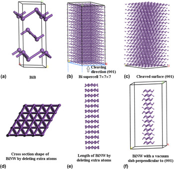
BiNW model was fabricated by following the steps. First, a 7 × 7 × 7 supercell of Bi crystal was built. Second, a surface along (001) plane was cleaved. Third, the atoms outside the cleaved surface were all deleted to obtain a nanowire with a cross section square of 1.13 nm2 and a length of 4.91 nm. Lastly, a vacuum slab of 10 Å was added perpendicular to the growth direction of BiNW. The modeling procedure is shown in Fig. 1.
Modeling procedure: (a) Bi bulk; (b) Bi supercell 7 × 7 × 7, cleaving direction along (001); (c) cleaved surface (001); (d) cross section shape of BiNW by deleting extra atoms; (e) length of BiNW by deleting extra atoms; (f) BiNW with a vacuum slab perpendicular to (001).

The electronic structure and the lattice dynamics were calculated by using CASTEP (Cambridge Serial Total Energy Package) of Materials Studio 8.0. Reference Segall, Lindan, Probert, Pickard, Hasnip, Clark and Payne21,Reference Kohn and Sham22 Norm-conserving pseudopotential was selected as pseudo-potential. Perdew–Burke–Ernzerhof parameters were adopted as the generalized gradient approximation (GGA) of Perdew. Reference Marlo and Milman23 Cutoff energy was adopted as 550 eV. The regular Monkhorst–Pack grid was sampled as 30 × 15 × 15 and 3 × 3 × 1 for BiB and BiNW, respectively. The high symmetry points of wave vector were selected as G (0.000, 0.000, 0.000) → F (0.000, 0.500, 0.000) → Q (0.000, 0.500, 0.500) → Z (0.000, 0.000, 0.500) → G (0.000, 0.000, 0.000). The influences of electron spin on the calculation of electronic structure were included. Reference Hammer, Hansen and Norkov24,Reference Franscis and Payne25 Before the calculation, a strict geometry optimization had been conducted according to the total energy, displacement, and stress. The partial density of states (PDOS) of electrons was achieved through broadening the discrete energy levels with a smearing value of 0.05 eV. Reference Monkhorst and Pack26
The electron transport was mainly determined by the bands ranging from −2 eV to +2 eV, in which the bands from −2 eV to Fermi level 0 eV were called valence band (VB) top where the carriers corresponded to electrons while the bands from 0 eV to +2 eV were called conduction band (CB) bottom where holes were the major carriers. As for a p-type semiconductor (the Fermi level was located in the VB top), the four nearest bands at the Fermi level in VB top were selected to calculate the band parameters. For an n-type semiconductor (the Fermi level was located in the CB bottom) the four nearest bands at the Fermi level in CB bottom were selected to calculate the band parameters. As for a semimetal, however, total four nearest bands across the Fermi level in CB bottom and VB top were selected to calculate the band parameters. The Fermi level of BiNW can be adjusted by tuning the cross section shape and length of BiNW or introducing quantum dots (defects or vacancies). The temperature dependence of the electron and phonon transport for BiB and BiNW was obtained by calculating the derivative of the Fermi-Dirac distribution function. The effective mass of carriers
 ${m^*}$
was achieved by differentiating the energy value E at Fermi level twice with respect to the wave vector as follows:
 $${m^*} = {{{\hbar ^2}} \mathord{\left/ {\vphantom {{{\hbar ^2}} {\left( {{{{\partial ^2}E} \over {\partial {k^2}}}} \right)}}} \right. \kern-\nulldelimiterspace} {\left( {{{{\partial ^2}E} \over {\partial {k^2}}}} \right)}}\quad ,$$
where ħ is Plank’s constant, E is the energy value, and k is the wave vector. The temperature dependency of phonon heat capacity was derived from phonon dispersion according to Eq. (3),
 $${C_\nu } = k\int {{{{{\left( {{{\hbar \omega } \over {kT}}} \right)}^2}\exp \left( {{{\hbar \omega } \over {kT}}} \right)} \over {{{\left[ {\exp \left( {{{\hbar \omega } \over {kT}}} \right) - 1} \right]}^2}}}} F(\omega )\,{\rm{d}}\omega \quad ,$$
where C ν is the phonon heat capacity, ω and F(ω) are the phonon vibration frequency and phonon density of states, T is the absolute temperature, k and ħ are Boltzmann’s constant and reduced Planck’s constant, respectively. Heat capacity in the Debye model was described as Eq. (4),
 $$C_\nu ^{\rm{D}}(T) = 9Nk{\left( {{T \over {{\Theta _{\rm{D}}}}}} \right)^3}\int_0^{\Theta {\rm{D}}T} {{{{x^4}{e^x}} \over {{{({e^x} - 1)}^2}}}\,{\rm{d}}x} \quad ,$$
where N was the number of atoms per cell. Consequently, the Debye temperature ΘD was achieved by calculating the actual heat capacity and then inverting into Eq. (3). The phonon mean free path λ was calculated in terms of Eq. (5),
 $$\lambda = {10^{ - 8}}\exp \left( {{{{\Theta _{\rm{D}}}} \over {\eta T}}} \right)\quad ,$$
where ΘD is the Debye temperature and η is a constant equal to 1.62 depending on the phonon scattering limitation. Reference Li, Wang, Wang, Peng, Zhang, Zhao, Liu, Zhang and Mei27,Reference Murata, Nakamura, Hasegawa, Komine, Taguchi, Nakamura, Jaworski, Jovovic and Heremans28 The Fermi level at 0 K was obtained according to Eq. (6),
 $$E_{\rm{F}}^0 = {{{\hbar ^2}k_0^2} \over {2{m^*}}} = {{k_0^2} \over 2}{{{\partial ^2}E} \over {\partial {k^2}}}\quad ,$$
where ħ and k
0 are reduced Plank’s constant and the sphere surface radius in k space,
 ${m^*}$
is the carrier effective mass, E is the energy value, k is the wave vector. The temperature dependency of the Fermi level E
F was obtained according to Eq. (7),
 $${E_{\rm{F}}} = E_{\rm{F}}^0\left[ {1 - {{{\pi ^2}} \over {12}}{{\left( {{{{k_{\rm{B}}}T} \over {E_{\rm{F}}^0}}} \right)}^2}} \right]\quad ,$$
where
 $E_{\rm{F}}^0$
is the Fermi level at 0 K, and T and k
B are the absolute temperature and Boltzmann’s constant respectively.
Reference Huang29
The derivative of the Fermi–Dirac distribution function
 $\left( { - {{\partial f} \over {\partial E}}} \right)$
was given as Eq. (8),
 $$\left( { - {{\partial f} \over {\partial E}}} \right) = {1 \over {{k_{\rm{B}}}T}}{1 \over {\left( {{e^{{{\left( {E - {E_{\rm{F}}}} \right)} \mathord{\left/ {\vphantom {{\left( {E - {E_{\rm{F}}}} \right)} {{k_{\rm{B}}}T}}} \right. \kern-\nulldelimiterspace} {{k_{\rm{B}}}T}}}} + 1} \right)}} \cdot {1 \over {\left( {{e^{ - {{\left( {E - {E_{\rm{F}}}} \right)} \mathord{\left/ {\vphantom {{\left( {E - {E_{\rm{F}}}} \right)} {{k_{\rm{B}}}T}}} \right. \kern-\nulldelimiterspace} {{k_{\rm{B}}}T}}}} + 1} \right)}}\quad ,$$
where k B and T are Boltzmann’s constant and the absolute temperature, E is the energy value, and E F is the Fermi level at a given temperature. The average velocity of carriers υe(E) was calculated through differentiating the energy value with respect to the wave vector, Reference Stiewe, Bertini, Toprak, Christensen, Platzek, Williams, Gatti, Müller, Iversen, Muhammed and Rowe30
 $${\upsilon _{\rm{e}}}\left( E \right) = {1 \over \hbar }{{\partial E} \over {\partial k}}\quad ,$$
where E is the energy value and k is the wave vector. Consequently, the electrical conductivity and the Seebeck coefficient were calculated in terms of Eqs. (10) and (11), Reference Wang, Tang, Long and Shuai31–Reference Peng, Wang, Li, Zhang, Wang and Sun33
 $$\sigma = {{{e^2}} \over 3}\int {{\rm{d}}E\left( { - {{\partial f} \over {\partial E}}} \right)} g\left( E \right)\tau \left( E \right){\upsilon ^2}\left( E \right)\quad ,$$
 $$\alpha = {e \over {3T\sigma }}\int {{\rm{d}}E\left( { - {{\partial f} \over {\partial E}}} \right)} g\left( E \right)\tau \left( E \right){\upsilon ^2}\left( E \right)\left( {E - {E_{\rm{F}}}} \right)\quad ,$$
where e is the electron charge,
 $\left( { - {{\partial f} \over {\partial E}}} \right)$
is the derivative of Fermi distribution function, g(E) is the density of states, υe(E) is the average velocity of carriers, E is the energy value, and E
F is the Fermi level at a given temperature. τ(E) is the relaxation time which could be regarded as an energy-independent constant.
Reference Nakamura, Murata, Hasegawa, Komine, Uematsu, Nakamura and Taguchi34
The electron thermal conductivity κe was obtained according to the Wiedemann–Franz law as follows
Reference Ashcroft and Mermin35,Reference Lv, Liu, Shi, Tang and Uher36
:
 $${\kappa _{\rm{e}}} = L\sigma T\quad ,$$
where L is the Lorentz constant equal to 2.45 × 10⁻⁸ V2/K2 and 1.5 × 10⁻⁸ V2/K2 for BiB and BiNW, respectively, σ is the electrical conductivity, and T is absolute temperature. The Lorenz number L depends on the scattering parameter and will decrease as the Fermi energy decreases with increasing temperature. To calculate the Lorenz number precisely, the carriers concentration and Seebeck coefficient should be measured firstly, and then the reduced Fermi energy is derived from the Seebeck coefficient by using Fermi integral. However, the Lorenz number L can also be estimated roughly. As for heavily doped strong degenerate semiconductor (with a high carriers concentration), the Lorenz number is selected as 2.45 × 10⁻⁸ V2/K2, for weak degenerate semiconductor as 2.0 × 10⁻⁸ V2/K2, and for non-degenerate semiconductor as 1.5 × 10⁻⁸ V2/K2. The phonon thermal conductivity κp was calculated according to Eq. (13), Reference Caillat, Kulleck, Borshchevsky and Fleurial37
 $${\kappa _{\rm{p}}} = {1 \over 3}\rho {\upsilon _{\rm{p}}}C\lambda \quad ,$$
where ρ is the theoretical density equal to 11,830 kg/m3 and 9325 kg/m3 for BiB and BiNW, respectively (BiB has a cell volume of 213 Å3 and total 12 atoms, and BiNW has a cell volume of 4796 Å3 and total 214 atoms). C is the heat capacity, and υp is the average velocity of phonons equal to 1883 m/s and 1065 m/s for BiB and BiNW, respectively. The average velocity of phonons was derived from the phonon dispersion by differentiating the phonon frequency with respect to the wave factor. Thus the ZT value was achieved according to Eq. (1).
III. RESULTS AND DISCUSSION
A. Electronic structure
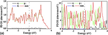
The partial density of states (PDOS) of BiB and BiNW is presented in Figs. 2(a) and 2(b), respectively. A typical semimetal characteristic for BiB is observed clearly due to the existed energy bands along the Fermi energy level. However, BiNW exhibits a typical semiconductor characteristic with a narrow band gap of about 0.4 eV. Such transition from semimetal (SM) to semiconductor (SC) is also observed in Bi quantum well. Reference Pichanusakorn and Bandaru38 In general, electric conductivity is mainly determined by the density of states (DOS) near Fermi energy level Reference Ziman39 according to the following formula:
 $$\sigma = {{n{e^2}\tau } \over m} = {{e\mu } \over {2{\pi ^2}}}{\left( {{{2{k_{\rm{B}}}T} \over {{\hbar ^2}}}} \right)^{{3 \mathord{\left/ {\vphantom {3 2}} \right. \kern-\nulldelimiterspace} 2}}}{\left( {{m^*}} \right)^{{3 \mathord{\left/ {\vphantom {3 2}} \right. \kern-\nulldelimiterspace} 2}}}{F_{{1 \mathord{\left/ {\vphantom {1 2}} \right. \kern-\nulldelimiterspace} 2}}}\quad ,$$
where n is the carrier concentration, e is the electron charge, m is carrier mass, τ is the scattering time of carriers, μ is the mobility of carriers,
 ${m^*}$
is the effective mass of carriers, k
B is Boltzmann’s constant, T is the absolute temperature, and ħ and F
1/2 are the reduced Plank’s constant and the Fermi–Dirac function of order one-half. Small DOS of 1.1 electrons/eV for BiB is a main reason for its small electrical conductivity. However, DOS of BiNW at Fermi energy level is increased significantly to 8.0 electrons/eV, which results in a high electrical conductivity. As for Seebeck coefficient, the effective mass of carriers is a main influencing factor according to the following formula
Reference Cutler, Leavy and Fitzpatrick40
:
 $$\alpha = {{8{\pi ^2}{k_{\rm{B}}}^2} \over {3e{h^2}}}{m^*}T{\left( {{\pi \over {3n}}} \right)^{{2 \mathord{\left/ {\vphantom {2 3}} \right. \kern-\nulldelimiterspace} 3}}}\quad ,$$
where n and
 ${m^*}$
are the concentration and effective mass of carriers, respectively. The calculated effective mass of carriers for BiB and BiNW is 0.012 m
e and 0.05 m
e at the top of valence band (VB), respectively, which is beneficial to an increased Seebeck coefficient for BiNW. In addition, it is also observed clearly that the electrons at the top of VB (from −2 eV to 0 eV) in BiB and BiNW mainly come from p-orbital and small from s-orbital. So, there exists only one s–p hybridization bonding behavior in BiB and BiNW, which will induce a continuous spectrum in their phonon density of states curve. Pseudogap energy, an energy difference between the nearest two peaks at the Fermi level in DOS curve, reflects the overlap of the electron clouds of the parent atoms. So the covalent bonding strength during bonding behavior can be evaluated by the obtained pseudogap energy qualitatively. It is clear that the pseudogap energy of 0.40 eV for BiNW is much smaller than BiB, which indicates a relatively weakened covalent bonding, a lowered phonon vibration frequency, and thus a suppressed phonon thermal conductivity according to the following formula:
 $$\omega = \sqrt {{k \over m}} \quad ,$$
where k is the bonding strength and m is the effective mass.
Density of states: (a) BiB; (b) BiNW.

B. Lattice dynamics
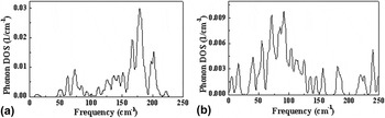
The phonon density of states for BiB and BiNW is shown in Figs. 3(a) and 3(b), respectively. A continuous spectrum can be observed in the phonon density of states curve for BiB and BiNW. Such a phenomenon is caused by the bond length distribution in the unit cell. Reference Menon, Richter and Subbaswamy41 The existed single s–p hybridization bonding between Bi atoms implies only one force constant, which leads to the observed continuous spectrum. Importantly, the maximum phonon density of states for BiNW is only 0.009 (1/cm−1), which will cause an obvious reduction in its phonon thermal conductivity.
Phonon density of states: (a) BiB; (b) BiNW.

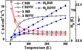
The temperature dependence of the heat capacity, the Debye temperature, and the mean free path for BiB and BiNW are shown in Fig. 4. The calculated heat capacity at room temperature is 10 cal/cell K and 36 cal/cell K for BiB and BiNW, respectively. The total heat capacity is divided into the phonon heat capacity (C p) and the electron heat capacity (C e). In a low temperature (below 100 K), the temperature dependency of heat capacity coincides with the formula C = AT 3, which belongs the C p. In a high temperature (above 100 K), however, the temperature dependency of heat capacity is positively proportional to AT, which is the C e. Heat capacity is a constant which is independent of the nature of materials according to the Dulong–Petit law. So the thermal transport in BiNW should follow the Debye theory. At a low temperature limit, the heat capacity is determined by the lowest phonon vibrational frequency and is written as follows:
 $${C_v}\left( {{T \mathord{\left/ {\vphantom {T {{\Theta _{\rm{D}}}}}} \right. \kern-\nulldelimiterspace} {{\Theta _{\rm{D}}}}}} \right) \to 9R{\left( {{T \over {{\Theta _{\rm{D}}}}}} \right)^3}\int_0^\infty {{{\xi {e^\xi }} \over {{{\left( {{e^4} - 1} \right)}^2}}}} {\rm{d}}\xi = {{12{\pi ^4}} \over {15}}R{\left( {{T \over {{\Theta _{\rm{D}}}}}} \right)^3},\;\left( {T \to 0\;{\rm{K}}} \right)\quad .$$
Heat capacity, Debye temperature, and mean free path as a function of temperature for BiB and BiNW.

Therefore heat capacity is positively proportional to T 3, which is also called as the T 3 law. Actually, the T 3 law is valid only at a very low temperature (T < ΘD/30). As for BiB and BiNW, their high Debye temperature results a high phonon vibrational frequency. In this case, the calculated heat capacity is smaller than the classical value. Debye temperature ΘD is described as the following formula:
 $${\Theta _{\rm{D}}} = {{\hbar {\omega _{\rm{m}}}} \over {{k_{\rm{B}}}}}\quad ,$$
where ħ is the Plank constant, ωm is the maximum vibrational frequency of phonons, and k B is Boltzmann’s constant. So, Debye temperature is determined only by the maximum vibrational frequency of phonons, which increases with temperature. It is seen that the Debye temperature for BiB and BiNW increases continuously with temperature. The calculated Debye temperature at room temperature is 890 K and 567 K, respectively. The decreased Debye temperature of BiNW means a lower vibrational frequency of phonons as compared to BiB, which is well consistent with the results of Figs. 3(a) and 3(b). Such decrease in Debye temperature for BiNW will result in a short mean free path. Mean free path of phonons, which is determined by the collision chance between phonons, is closely related to temperature T. At a high temperature (T ≫ ΘD) the amount of phonons is proportional to temperature T, which results in a negative temperature dependency of mean free path. However, at a lower temperature (T ≪ ΘD), the mean free path is defined as follows:
 $$\lambda \propto {e^{{{{\Theta _{\rm{D}}}} \mathord{\left/ {\vphantom {{{\Theta _{\rm{D}}}} {aT}}} \right. \kern-\nulldelimiterspace} {aT}}}}\quad ,$$
where ΘD is the Debye temperature, a is a constant ranging from 2 to 3, and T is absolute temperature. It is seen that the mean free path of phonons decreases sharply with increasing temperature, which is explained by the decreased phonons with a short wave length during the collision process. The mean free path at 300 K for BiB and BiNW is 5.9 × 10⁻⁸ m and 3.2 × 10⁻⁸ m, respectively. So an obvious reduction in phonon thermal conduction is expected for BiNW.
C. Thermoelectric properties
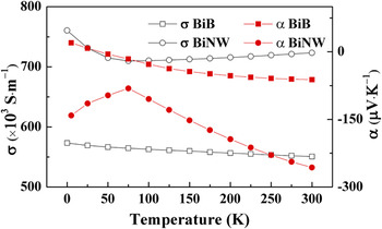
The electrical conductivity and Seebeck coefficient as a function of temperature for BiB and BiNW are presented in Fig. 5. It is found that the electrical conductivity of BiB decreases continuously with increasing temperature, indicating a typical semimetal characteristic. However, BiNW exhibits a typical semiconductor behavior due to its positive temperature dependence of the electrical conductivity above a high temperature (100 K), which coincides with the experimental results of Bi nanowire with a diameter of 7 nm. Reference Heremans, Thrush, Lin, Cronin, Zhang, Dresselhaus and Mansfield42 In fact, such transition between semimetal and semiconductor had been observed in Bi nanotubes. Reference Zhou, Li and Li43 In fact, the temperature dependence of the electrical conductivity of Bi nanowires changes significantly with the different diameter size. Reference Murata, Tsunemi, Saito, Shirota, Fujiwara, Hasegawa and Komine9 The obtained electrical conductivity of 723,000 Ω−1/m at 300 K for BiNW is slightly smaller than the experimental 800,000 Ω−1/m at 300 K of BiNW, Reference Nakamura, Murata, Hasegawa, Komine, Uematsu, Nakamura and Taguchi34 but is close to the value of BiNW with a diameter of 7 nm. Reference Heremans, Thrush, Lin, Cronin, Zhang, Dresselhaus and Mansfield42 In comparison with BiB, such enhancement in electrical conductivity for BiNW is originated from its largely enhanced density of states near the Fermi energy level. On the other hand, the negative sign of Seebeck coefficients for BiB and BiNW indicates that the major carriers are electrons, and the obtained temperature dependence above 75 K of the Seebeck coefficient for BiNW is close to the experimental value of Bi nanowire. Reference Nakamura, Murata, Hasegawa, Komine, Uematsu, Nakamura and Taguchi34 Moreover, the Seebeck coefficient for BiNW at 300 K is largely improved to 253 μV/K as compared to BiB, which is close to the data of Bi nanomaterials. Reference Lin, Sun and Dresselhaus18 Such improvement in Seebeck coefficient for BiNW is attributed to its increased effective mass of carriers, the reduced Fermi level, and the scattering parameters. In further, the Seebeck coefficient of BiNW could be improved obviously by decreasing the diameter size.
Electrical conductivity and Seebeck coefficient as a function of temperature for BiB and BiNW.

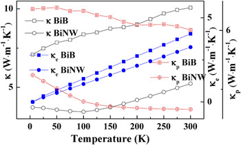
Figure 6 plots the total, electron, and phonon thermal conductivity of BiB and BiNW as a function of temperature. It is clear that BiNW exhibits a typical positive temperature dependence of the thermal conductivity, which has been observed in Bi nanowire with a diameter of 10 nm. Reference Hasegawa, Murata, Tsunemi, Saito, Shirota, Komine, Dames and Garay44 It is also found that the total thermal conductivity κ of BiNW at 300 K is reduced to 5.3 W/(m K), which is larger than the experimental 2.5 W/(m K) of BiNW with a diameter of 10 nm but is close to that of the BiNW with a diameter of 320 nm. Reference Roh, Hippalgaonkar, Ham, Chen, Li, Ercius, Majumdar, Kim and Lee7 It should be noted that the thermal conductivity of BiNW could be further reduced significantly as the diameter size is smaller than the phonon mean free path. Reference Kim, Kim, Choi and Kim12 Generally κ is divided into two parts: the electron thermal conductivity κe and the phonon thermal conductivity κp. The κe of BiNW and BiB increases steadily with increasing temperature and the obtained value at 300 K is 3.3 W/(m K) and 5.3 W/(m K), respectively. The observed positive temperature dependence of κe is resulted from the increased concentration of carriers with increasing temperature while the enhanced κe in BiNW is attributed to its large electrical conductivity as compared to BiB. It should also be noted that the κp for BiNW and BiB exhibits a negative temperature dependence over the whole temperature. Moreover, the κp of BiNW [2.0 W/(m K)] is largely reduced by a factor of 2 as compared to BiB [6.0 W/(m K)]. It is well known that the κp is closely related to the mean free path of phonons. At a temperature above Debye temperature, the amount of phonons is positively proportional to temperature T according to the following formula:
 $$n = {1 \over {{e^{{{\hbar \omega } \mathord{\left/ {\vphantom {{\hbar \omega } {{k_{\rm{B}}}T}}} \right. \kern-\nulldelimiterspace} {{k_{\rm{B}}}T}}}} - 1}} \approx {{{k_{\rm{B}}}T} \over {\hbar \omega }}\quad ,$$
where n is average phonon amount, k B and T are Boltzmann’s constant and absolute temperature, ħ is reduced Plank’s constant, and ω is the vibrational frequency of phonons. As a result, the average phonon amount increases with increasing temperature, which results in a more frequent collision of phonons and thereby a decreased mean free path of phonons. Thus, the observed negative temperature dependence of the κp is caused by an increased average phonon amount in a higher temperature. Reference Huang45 Generally when the diameter of a nanowire is smaller than its phonon mean free path, the phonon thermal conductivity of the nanowire is lower than its bulk counterpart because of phonon boundary scattering. Reference Li, Wu, Kim, Shi, Yang and Majumdar13 The dominant mechanisms which profoundly influence on the phonon thermal conductivity are phonon–phonon scattering, charge-carrier-phonon scattering, and point-defect–phonon scattering. At a low temperature, the phonon–phonon scattering and the point defect scattering are the most important factors in reducing the phonon thermal conductivity for short wavelength phonons of BiB, while the electron–phonon scattering is more effective for long wavelength phonons at a higher temperature. Reference Bux, Blair, Gogna, Lee, Chen, Dresselhaus, Kaner and Fleurial46 As for BiNW, however, the phonon scattering plays an important role at both long and short wavelengths, which leads to a large reduction in phonon thermal conductivity due to the decreased phonon DOS, the lowered phonon vibration frequency, and the shortened mean free path of phonons. Reference Moore, Pettes, Zhou and Shi19,Reference Henry and Chen47
Total, electron, and phonon thermal conductivity as a function of temperature for BiB and BiNW.

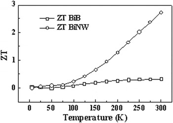
Figure 7 shows the figure of merit ZT as a function of temperature for BiB and BiNW. The ZT at 300 K of BiNW can be enhanced to 2.73 by a factor of 8 as compared to BiB, which is smaller than the predicted value of BiNW by Lin et al. Reference Hicks, Harman and Dresselhaus17,Reference Lin, Sun and Dresselhaus18 Such large enhancement in ZT for BiNW is attributed to its largely increased electrical conductivity, Seebeck coefficient, and meanwhile significantly suppressed phonon thermal conductivity. In addition, with the diameter size decreasing, the Seebeck coefficient of BiNW will be increased further while the thermal conductivity will be suppressed largely, and consequently the figure of merit could be optimized to the most extreme. Reference Shi, Yao, Zhang and Li11
Figure of merit as a function of temperature for BiB and BiNW.

IV. CONCLUSIONS
Summing up, the electronic structure, the lattice dynamics, and the thermoelectric properties of BiB and BiNW have been calculated successfully through first-principles and Boltzmann’s transport theory. A typical transition from semimetal (BiB) to semiconductor (BiNW) is observed. In comparison with BiB, the density of states at Fermi energy level for BiNW is increased while its pseudogap and the phonon density of states are all decreased. Moreover, BiNW possesses an increased heat capacity, a lowered Debye temperature, and a reduced mean free path of phonons. The electrical conductivity and Seebeck coefficient at 300 K for BiNW are increased while its total and phonon thermal conductivity is suppressed significantly. As a result, a largely enhanced ZT value of 2.73 at 300 K is achieved for BiNW. The enhancement in electrical conductivity and Seebeck coefficient of BiNW is originated from its large density of states and effective mass of carriers, but its significant reduction in thermal conductivity is ascribed to the lowered vibration frequency, the reduced phonon amount, and the decreased mean free path of phonons. Therefore BiNW should be viewed as an excellent candidate for a thermoelectric material with a high figure of merit.
ACKNOWLEDGMENT
This work was financially supported by Science Foundation of Henan University of Technology under Grant No. 2015XTCX10.