Introduction
The rapid progress in electronics and wireless communications over the past decades has led to a growing demand for wireless devices with the ability to operate at visible and infrared (IR) regimes. This enables miniaturization of devices and circuits usually operating at much lower frequencies.
The optical wireless nanolinks offer a better performance in sending optical signals from one point to the other as they do not suffer from the losses associated with the waveguide interconnect counterparts, especially when the propagation distance is of the order of several wavelengths.[Reference Alù and Engheta1, Reference Yang, Li and Qiu2] They can also provide simpler and ultracompact network architectures. The high directionality of antennas is a key parameter in the performance of such wireless links and networks.
In nanophotonics, highly directional antennas have been realized using arrays of plasmonic and dielectric nanoantennas as well as impedance sheets arranged based on the phased array,[Reference Ahmadi, Ghadarghadr and Mosallaei3] Yagi-Uda,[Reference Maksymov, Staude, Miroshnichenko and Kivshar4] and holographic design[Reference Patel and Grbic5] approaches. In these cases, while individual elements of the arrays are subwavelength, the overall size of the antenna system becomes greater than the radiation wavelength.
As such, downscaling of the whole radiative system to subwavelength footprints is a challenge that needs to be tackled. Semiconductor quantum dots as point-like dipole sources of spontaneous emission are promising candidates to surmount this challenge, but achieving a high radiation efficiency and directionality require nanoantennas in order to effectively match the impedance of a quantum source to that of free space. Plasmonic and high-index semiconductor nanoantennas can be used for this purpose as they are able to manipulate light at the nanoscale while controlling the far-field emission.
A large number of works have utilized resonant plasmonic structures such as bowties, dimers, and film-coupled nanoparticles due to their ability to capture and concentrate the light at subwavelength dimensions.[Reference Kinkhabwala, Yu, Fan, Avlasevich, Müllen and Moerner6, Reference Ureña, Kreuzer, Itzhakov, Rigneault, Quidant, Oron and Wenger7] Accurate placement of nanoemitters in the high-field regions of these structures provides a flexible means of controlling the emission. Typical drawbacks of plasmonics include the large ohmic losses associated with metals at optical frequencies as well as limited control over the directionality of emission.[Reference Vercruysse, Sonnefraud, Verellen, Fuchs, Martino, Lagae, Moshchalkov, Maier and Dorpe8]
More recently, particles of high refractive index dielectric materials have been investigated for nanophotonics applications as alternative platforms to plasmonic materials. These materials offer practical benefits because of their cheap cost and the capability of using mature semiconductor fabrication techniques while possessing lower energy loss compared with plasmonics due to the absence of free-electron absorption.[Reference Evlyukhin, Reinhardt, Seidel, Luk'yanchuk and Chichkov9] Moreover, rotation of the displacement current can give rise to magnetic resonances in simple structures of dielectric materials,[Reference Garcia-Etxarri, Gómez-Medina, Froufe-Pérez, López, Chantada, Scheffold, Aizpurua, Nieto-Vesperinas and Sáenz10] whereas plasmonic particles require complicated structures such as split-ring resonators to excite magnetic resonances. Interference of magnetic and electric dipole resonances inside all-dielectric nanoantenna systems is shown to lead to directional and wavelength-dependent scattering patterns. This can be achieved, for example, in an asymmetric dimer.[Reference Albella, Shibanuma and Maier11] For a single dielectric nanoparticle, a balanced excitation of electric and magnetic dipoles, as well as higher order modes excitation can lead to highly directional patterns.[Reference Fu, Kuznetsov, Miroshnichenko, Yu and Luk'yanchuk12–Reference Krasnok, Simovski, Belov and Kivshar14] Excitation by a near-by quantum emitter was found to provide the necessary asymmetry for the excitation of higher order modes in subwavelength dielectric nanoparticles, which enhances the directivity in these configurations without a significant increase of the antenna size.[Reference Krasnok, Simovski, Belov and Kivshar14]
In addition to the interference between the illumination dipole and the multipolar modes of the nanoantenna, the presence of a layered substrate can also induce symmetry breaking in the far-field pattern.[Reference Novotný and Hecht15, Reference Coenen, Bernal Arango, Femius Koenderink and Polman16] Multilayer substrates allow the development of multi-lobed patterns due to the interference effects that can effectively reshape the radiation pattern of a dipole emitter.[Reference Novotný and Hecht15] The radiation pattern can be further influenced by the addition of a nanoantenna. By adding a subwavelength nanoantenna as a passive element at a well-chosen position with respect to a dipole emitter above a layered substrate, it is possible to achieve directional radiation patterns.[Reference Coenen, Bernal Arango, Femius Koenderink and Polman16]
While the majority of previous theoretical studies considered isolated nanoparticles in free space, for all practical applications particles are placed on a substrate. Moreover, coupling to the substrate can be favorably exploited. Engineering the substrate provides an additional degree of freedom in tailoring scattering through interference, retardation and screening effects.[Reference van de Groep and Polman17–Reference Markovich, Ginzburg, Samusev, Belov and Zayats19] Layered platforms and heterostructures can also enable the realization of active nanoantenna systems whose steering angle can be controlled electromechanically, or electro-optically in real time through the employment of nanoactuators or electro-optical materials, such as transparent conductive oxides and graphene. Such tunability mechanisms have been exploited recently in reflect-array[Reference Huang, Lee, Sokhoyan, Pala, Thyagarajan, Han, Tsai and Atwater20–Reference Momeni Hasan Abadi, Booske and Behdad23] and leaky-wave antennas[Reference Cheng, Jafar-Zanjani and Mosallaei24, Reference Esquius-Morote, Gomez-Diaz and Perruisseau-Carrier25] to achieve beam steering based on the phased array and holography concepts.
The present work is inspired by the paramount importance to actively steer the beaming angle in the radiation pattern of quantum emitters coupled to nanoantennas. Such tunability is of great interest in the optical wireless networks as it provides more flexibility in the position of the receiver and switching between different communication channels. To this end, we use nanowire antennas that have played a crucial role in the development of a new generation of optical platforms. Recent advances in drawing and lithography techniques have allowed for the fabrication of laterally oriented nanowires on various substrates incorporating different material compositions.[Reference Burke, Carrad, Gluschke, Storm, Fahlvik Svensson, Linke, Samuelson and Micolich26, Reference Duan, Huang, Cui, Wang and Lieber27] Moreover, fabrication of layered structures of two-dimensional (2D) and bulk materials have been widely accomplished providing an endless opportunity for combining different materials that can enable new functionalities and tune the optical properties of the substrate. Here, we consider a silicon nanowire antenna on a layered substrate, excited by a near-by point source. We incorporate nanoactuators, transparent conductive oxides, and graphene into the substrate, respectively, to realize tunable platforms in visible, near-IR (NIR), and far-IR (FIR) frequency regimes. To this purpose, we leverage substrate-induced interference effects and tunability mechanisms. Each configuration is optimized to achieve maximal steering range while attaining a proper gain which is the enhancement ratio of radiation intensity in the beaming direction with respect to isotropic radiation intensity. The interference effects allow to obtain a high gain in subwavelength antenna systems, exceeding the limit of dipolar modes in subwavelength particles.[Reference Coenen, Bernal Arango, Femius Koenderink and Polman16] To avoid the use of computationally expensive numerical methods, we develop an efficient and accurate semi-analytical framework based on transition matrix (T-matrix) formulation, which facilitates detailed quantification and optimization of the far-field radiation patterns through closed-form solutions. Moreover, the method can give more insight into the physical phenomena by separating different field contributions to the radiation pattern. It should be noted that the antenna systems devised in this work are subwavelength and very different from phased arrays and Yagi–Uda antennas whose sizes are large compared with the wavelength. The proposed platforms are ideal candidates for nanoantenna synthesis in optical wireless networks due to their subwavelength footprint, enhanced directionality, real-time tunability, and fairly simple geometry.
Methods
The drawing and lithography techniques provide a good control over the length and diameter of nanowires. While the radius of a nanowire is usually in nanometer scale, the ratio of length to diameter can be as large as 100–1000 making the length significantly larger than the operating wavelengths. This enables us to study the scattering of light from nanowires using 2D cylindrical models. The problem of scattering from cylindrical structures has been studied for many years and several different methods have been employed for this purpose. Adopting brute-force numerical methods inevitably leads to numerical models with an enormous number of unknowns, considering small geometrical features that necessitate ultra-fine meshing. Therefore, semi-analytical methods that exploit some available geometrical features of the structure can be of great advantage. These methods rely on the multipole expansions, among which the T-matrix method is the most powerful. Recently, there have been several attempts to extend the T-matrix formulation.[Reference Mishchenko, Zakharova, Khlebtsov, Videen and Wriedt28] In Ref. Reference Salary, Nazari and Mosallaei29, the T-matrix formulation was extended to the case of nanowire arrays above a layered substrate. However, the analysis was limited to ideal 2D problems where the incidence is a plane wave invariant in the wire axis direction. A generalized matrix formulation based on multipole expansion was proposed in Ref. Reference Salary, Jafar-Zanjani and Mosallaei30 to account for conical scattering from fibers and wire structures.
Despite the dramatic evolving of the T-matrix method, the problem of dipolar scattering from cylindrical structures has remained unaddressed as-yet and all the previous works have been concerned with scattering of plane waves. For a nanowire placed on a layered substrate excited by a near-by point source, the problem turns out to be much more difficult to deal with since it involves a cylindrical scatterer, a planar interface, and a spherical source; so all three coordinates in one problem, which leaves an interesting challenge for the semi-analytical solution. This requires multiple translations between these coordinate systems and handling slowly convergent highly oscillating integrals of Weyl and Sommerfeld types.
Here, building on the developments in Refs Reference Salary, Nazari and Mosallaei29 and Reference Salary, Jafar-Zanjani and Mosallaei30, we develop a general method that enables us to treat all types of wire structures excited by dipole emitters above layered substrates. To this purpose, we use Sommerfeld and Weyl identities to express different field contributions to the scattering, which are essentially spherical waves as a spectrum of cylindrical multipole expansions. All the cylindrical multipoles are then translated into the center of a nanowire using Graf's addition theorem and the boundary conditions are enforced subsequently to obtain unknown coefficients in the multipole expansion of the scattered field. Once the unknown coefficients are obtained, the stationary phase method is used to obtain asymptotic approximations of the field contributions in the far field, which facilitates detailed quantification and optimization of the far-field radiation patterns through closed-form solution. The detailed derivation of the field contributions to the scattering and their closed-form expressions is rather technical and is brought into the Supplemental Material. The validity of the proposed semi-analytical framework is also comprehensively studied and verified through comparison with finite-difference time-domain full-wave simulations for different configurations, which can be found in Supplemental Material. The proposed semi-analytical framework can also be readily extended to the interaction of dipolar sources with periodic and aperiodic gratings of nanowires above layered substrates. Despite the sophisticated treatment required by the method, it offers a significant advantage over brute-force methods in terms of computational complexity and efficiency. Moreover, it can provide insight into the physical phenomena by separating different field contributions.
In the following, we employ the developed semi-analytical framework to design and propose substrate-supported wire antenna platforms with the capability of real-time tunability and beam steering in the visible, NIR and FIR regimes through the application of nanoactuators and electro-optical materials, namely indium tin oxide (ITO) and graphene. The maximum number of cylindrical harmonics used for the truncation of the multipole expansions is chosen as M = 7, which ensures the convergence of the results for the subwavelength wire antennas. We consider a silicon nanowire antenna on a grounded layered substrate, excited by a near-by point source. The back mirror underneath the substrate ensures that all the light is emitted into the upper hemisphere. In this way, we minimize the large radiation loss associated with directive emission into the substrate upon increasing of the local density of states.
The interference effects of the substrate and the symmetry breaking of the nanowire scattering are engineered to obtain directional patterns in radiation. The electromechanical and electro-optical mechanisms are then exploited to steer the beam via changing the length of optical path between multipoles and their induced images into the ground plane. Thanks to the efficiency of the proposed method, each configuration is optimized in such a way that the maximal steering range is obtained while attaining a proper gain. The antenna gain is defined as the radiation intensity in the main beam direction, to the radiation intensity that would be obtained if the dipole emitter was radiating without the presence of the nanowire and the substrate (i.e., isotopically).
It has been previously established that in order to excite resonances in electrically small cylindrical configurations, the polarization of the exciting field has to be transverse electric (TE).[Reference Thorsen and Arslanagić13] Moreover, due to the 2D geometry of a nanowire antenna, a unidirectional directive emission can only be achieved in the plane perpendicular to the nanowire axis. As such, manipulation of radiation from a TE-polarized dipole, which has the widest beam pattern in this plane (a uniform circular pattern), is more critical for increasing the efficiency. Therefore, the polarization of the dipole source in the present work is chosen parallel to the wire axis. In all our designs, the quantum dot emitter radius is assumed to be λ/20 (with λ being the peak emission wavelength of the emitter), which is modeled by a point source located λ/20 above the substrate with a polarization along the nanowire axis (s-polarized dipole moment).
In principle, the spontaneous emission from a quantum dot is unpolarized and spans over a range of wavelengths while exhibiting a relatively narrow bandwidth. The unpolarized emission can be regarded as the average of radiation by two orthogonally polarized dipole moments. The proposed antenna systems here can only manipulate and enhance the directionality of s-polarized dipole radiation along azimuthal angle (φ) in the H-plane cut (i.e., the plane perpendicular to the nanowire axis θ = π/2) due to the subwavelength size and the 2D geometry of the nanowire antennas. Control over both polarizations and beam manipulation along both φ and θ angles can be achieved by using a 3D nanoantenna such as a nanosphere; however, nanowires are more favorable in terms of fabrication and integrability with optoelectronic devices.
Electromechanical tunability in visible regime
Although there is not yet a promising electro-optical material with a tunable refractive index in the visible light range, nanoactuators open up the possibility of voltage-controlled electromechanical tuning of the antenna platforms[Reference Momeni Hasan Abadi, Booske and Behdad23, Reference Holsteen, Raza, Fan, Kik and Brongersma31] and metamaterials[Reference Unlu and Jarrahi32, Reference Zhao, Fan, Zhang, Keiser, Duan, Averitt and Zhang33] in this regime. Nanoactuators can be realized by using different actuation mechanisms including electrostatic, piezoelectric, thermal, and magnetic.
Here, we provide evidence for an electromechanical tuning mechanism that can steer the beaming angle of a nanowire antenna operating in the visible spectral range. The tuning mechanism relies on electromechanically displacing a movable frame and changing an out-of-plane gap using an electrostatic comb drive.
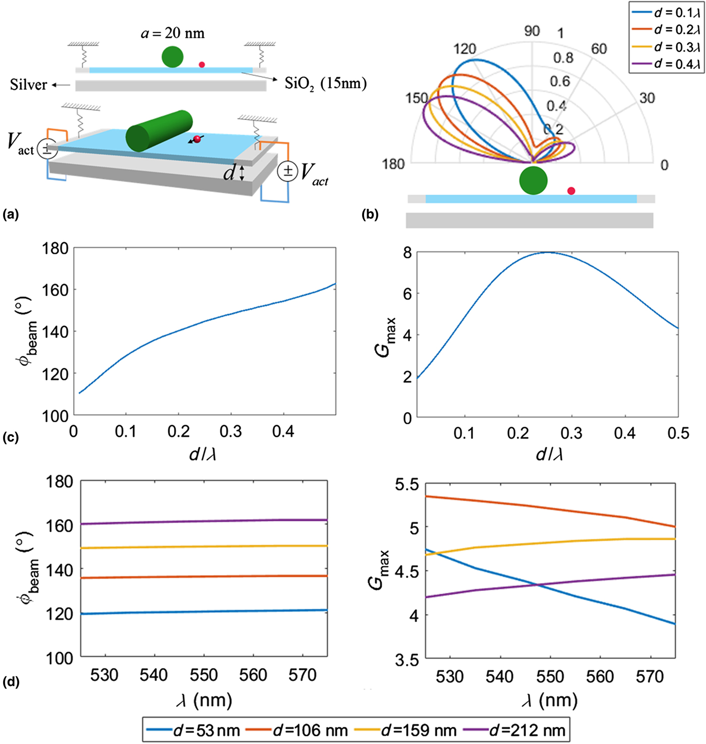
The schematic of the proposed structure is shown in Fig. 1(a). The silicon nanowire antenna and the quantum emitter are deposited on a movable silica frame separated from a silver back mirror. The movable frame can be actuated using a nanoactuator. A pair of side electrodes fixed to an elastic compensator can be used as contact pads for the actuator. The gap between the movable frame and the fixed ground plane can then be controlled with an applied voltage. The displacement can be estimated as a function actuation voltage as [Reference Yakovlevich Prinz, Alexandrovich Seleznev, Victorovich Prinz and Vladimirovich Kopylov34]:
 $$V_{{\rm act}} = \sqrt {\displaystyle{{8k} \over {27\varepsilon _0 A}}d_{}^3}, $$
where A is the actuation pad area, d is the gap between the actuation pad and the frame, and k is the spring constant of the actuator.
(a) The schematic of the proposed design for electromechanical tuning of the radiation of a dipole emitter coupled to a nanowire antenna in the visible light range. (b) Radiation pattern of the nanoantenna for different gap distances. (c) Beam angle and the gain of the nanoantenna as a function of gap distance. (d) Angular dispersion and gain variations of the antenna system in a bandwidth of 50 nm.
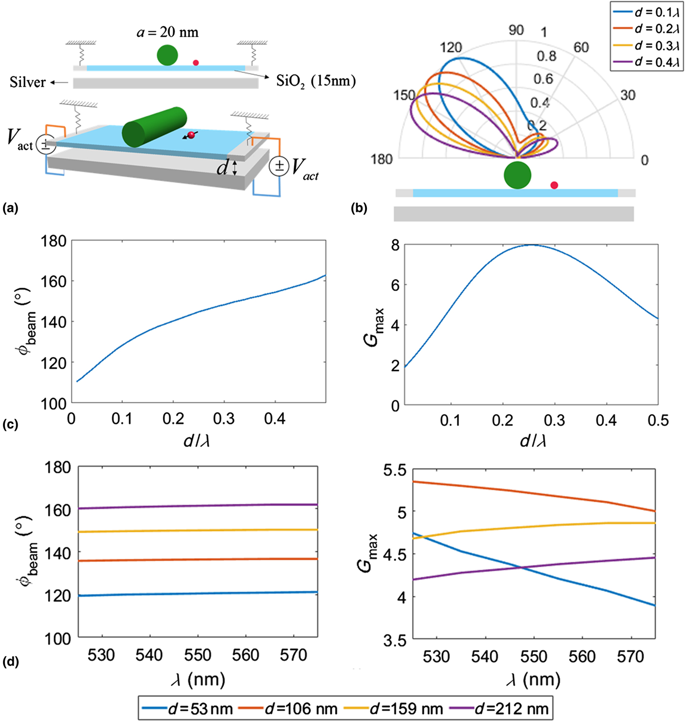
The peak emission wavelength is assumed to be λ = 532 nm corresponding to the green light. The optical constants of silicon and silica are taken from Ref. Reference Palik35 and those of the silver are taken from Ref. Reference Johnson and Christy36. The rest of the geometrical parameters are optimized and chosen in order to achieve a directive beam with maximal steering range by changing the out-of-plane gap while attaining a proper gain. The radius of the nanowire antenna is chosen as a = 20 nm, the thickness of the silica frame is set as 15 nm and the lateral distance between the nanowire antenna and quantum dot centers is considered 220 nm. The results of the radiation pattern in the H-plane for different values of the separation gap are depicted in Fig. 1(b). As it can be seen, directive radiation is achieved using an ultra-subwavelength nanowire antenna while the beaming direction is tunable by changing the out-of-plane gap between the silica frame and the silver back mirror and consequently changing the optical distance between the multipoles and their induced images into the ground plane.
The beaming angle and the gain of the antenna are shown in Fig. 1(c). According to the results, the beaming angle can be continuously tuned within a wide angular range of 50° while attaining a reasonably good gain. Further increasing the gap distance results into larger side lobes and undesirable secondary beams, which limit the steering range of the directional beam. The gap distance also changes the antenna gain by changing the strength of the electric field driving the antenna. The variations of the gain follow the Fabry–Pérot oscillations and the maximum is observed around the Fabry–Pérot resonance d/λ ≈ 0.25.
The spontaneous emission from a quantum dot emitter spans over a range of wavelengths while exhibiting a narrow bandwidth. As the beam steering mechanism depends on the optical length of the gap, the beaming angle is expected to change with the wavelength giving rise to angular dispersion. Considering that the emission bandwidth of quantum dots in the visible light spectrum is in the range of 20–50 nm, we study the angular dispersion and gain variations of the antenna system in such a narrow bandwidth. The results are plotted in Fig. 1(d) for different gap distances corresponding to the values chosen in Fig. 1(b). The required voltages to achieve these distances depend on the actuation pad area and spring constant of the actuator according to Eq. (1). As it can be seen, the change in the beaming angle is negligible in this bandwidth (~2°) as the optical length of the gap does not change significantly. Moreover, the trend in the gain variations shows that by increasing the gap distance, the gain peak is shifted to longer wavelengths.
Electrical tunability in NIR regime
Carrier-induced changes via gate biasing offer a route for refractive index modification in the doped semiconductors; however, the change is not significant in conventional semiconductors. Transparent conducting oxides such as ITO and indium zinc oxide are degenerately doped semiconductors that are commonly used as transparent electrodes in optoelectronic devices. They have carrier densities in the 1021–1023 cm−3 range where changes in carrier density yield strong changes in the refractive index in the NIR.[Reference Huang, Lee, Sokhoyan, Pala, Thyagarajan, Han, Tsai and Atwater20] This feature has made these materials ideal candidates for creating active building blocks for optical devices.[Reference Huang, Lee, Sokhoyan, Pala, Thyagarajan, Han, Tsai and Atwater20, Reference Forouzmand and Mosallaei21]
Here, we present a nanowire antenna operating in NIR on a layered substrate to which an ITO layer is added to achieve the electrical tunability in real time. The peak emission wavelength is chosen as λ = 1.55 μm corresponding to the telecommunication wavelength.
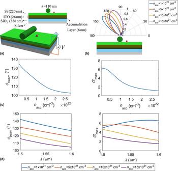
The schematic of the structure is shown in Fig. 2(a). The silicon nanowire antenna and the quantum dot emitter are placed on top of a layered structure backed by a silver mirror. An ITO layer is sandwiched between a doped silicon layer and an insulator namely SiO2. Using the silicon and the back mirror as contact pads for applying the electrical voltage across the ITO layer, a charge accumulation layer is formed at the ITO–SiO2 interface, increasing the ITO's carrier density, which changes the refractive index of this layer. Despite the significant changes in the refractive index of the accumulation layer with the applied voltage, the low dimensionality and small thickness of the accumulation layer requires enhanced light–matter interactions to make any appreciable changes in the optical response. As such, ITO-integrated devices are designed with high modal confinement. Here, we set the parameters of the layered heterostructure to couple into a Fabry–Pérot resonance having a high spatial overlap with ITO accumulation layer. This is achieved by choosing the thicknesses of the silicon and silica layers as 220 and 388 nm, respectively. In this case, the optical response is sensitive to even the slightest changes in the carrier density of the accumulation layer. The ITO layer thickness is considered to be 26 nm. The background and accumulation ITO layers are modeled with a Drude model  $\varepsilon = \varepsilon _0 [ {\varepsilon _\infty - \omega _{\rm p}^2 ( {\omega ( {\omega + i\Gamma} )} )^{ - 1}} ]$ with ε∞ = 2.17 and Γ = 190 THz.[Reference Forouzmand and Mosallaei21] The plasma frequency is related to the carrier density N and the electron effective mass m* = 0.35 × m 0 as
 $\omega _{\rm p}^2 = Ne^2 /\left( {\varepsilon _0 m^ * } \right)$, where e is the electron charge and m 0 is the electron rest mass. In accordance with the experimental data provided in Ref. Reference Feigenbaum, Diest and Atwater37, the background carrier concentration of ITO is chosen as n = 1021 cm−3 while assuming that the carrier concentration can be increased up to n acc = 2.83 × 1022 cm−3 in an accumulation layer with a thickness of 6 nm by applying a voltage.
(a) The schematic of the ITO-integrated design for electrical tuning of the radiation of a dipole emitter coupled to a nanowire antenna in the NIR regime. (b) Radiation pattern of the nanoantenna for different carrier concentrations in the experimentally accessible range. (c) Beam angle and the maximum gain of the nanoantenna as a function of carrier concentrations. (d) Angular dispersion and gain variations of the antenna system in a bandwidth of 100 nm.
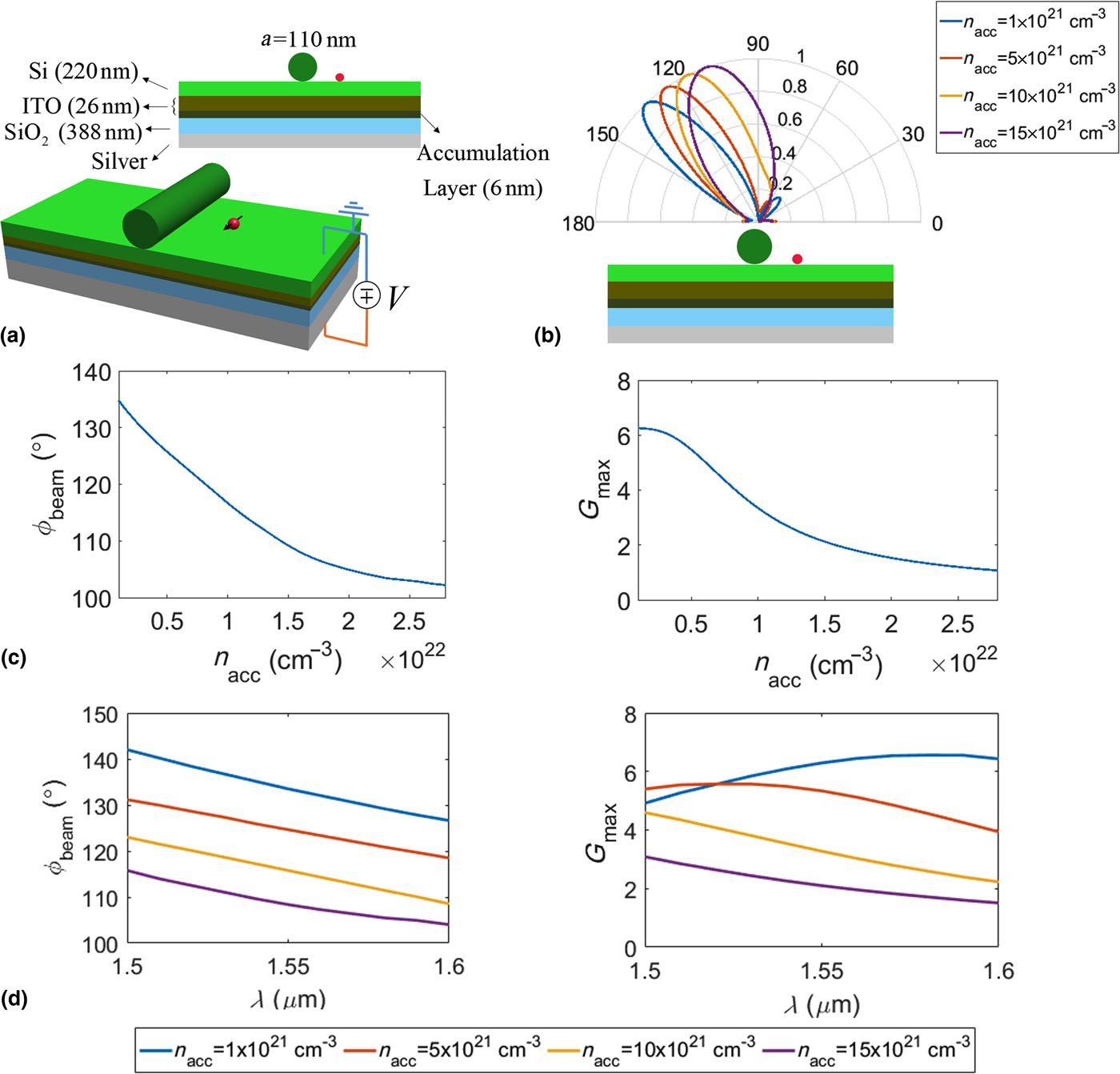
The rest of the structural parameters in the design are chosen to achieve a directive pattern with maximal tunability and proper gain. The radius of the silicon nanowire antenna is chosen as a = 110 nm, and the lateral distance between the nanowire antenna and quantum dot centers is set as 600 nm. Figure 2(b) shows the results for the radiation pattern of the nanoantenna in the H-plane for different carrier concentrations in the experimentally accessible range provided in Ref. Reference Feigenbaum, Diest and Atwater37. Directive beams are obtained while being tunable by changing the carrier concentration of the accumulation layer. Similar to the previous case, the underlying principle for tuning the radiation pattern can be attributed to the change in the optical distance of the multipoles and their induced images into the ground plane. As the carrier concentration in the accumulation layer increases, the relative permittivity decreases toward more negative values and it becomes closer to a metal thus shrinking the effective thickness of dielectric spacers and consequently the optical path between the multipoles and their induced images. Comparing Figs. 2(b) and 1(b), it can be verified that the effect of increasing the carrier concentration in the accumulation layer is similar to decreasing the gap distance.
The beaming angle and the maximum gain of the antenna are shown in Fig. 2(c) in terms of carrier concentration in the accumulation layer. According to the results, the beaming angle can be continuously tuned within an angular range of 30° while attaining a reasonably good gain. The radiation pattern reaches a steady state after some point such that further increasing the carrier concentration would not affect the response in the account of accumulation layer becoming a near-perfect metal layer. It should be mentioned that the charge distribution within the accumulation layer has an exponential decay profile where the decay length (effective thickness) is dependent on the physical properties of ITO. The accurate consideration of this fact may impact the beam steering range proportional to the effective thickness of accumulation layer.
The dispersion of the ITO material leads to angular dispersion in beam steering. The angular dispersion and the gain variations of the antenna system are plotted in Fig. 2(d) for different carrier concentrations in the accumulation layer in a bandwidth of 100 nm. The emission angle divergence is around 12° in this bandwidth, while the gain peak is shifted to shorter wavelengths by increasing the carrier concentration in the accumulation layer.
Electrical tunability in the FIR (low-THz) regime
Graphene as a 2D material provides a unique platform for actively tuning the optical devices operating over a wide spectral range from NIR to FIR regimes.[Reference Sherrott, Hon, Fountaine, Garcia, Ponti, Brar, Sweatlock and Atwater22–Reference Esquius-Morote, Gomez-Diaz and Perruisseau-Carrier25] The optical conductivity of graphene depends on the chemical potential that can be changed via chemical doping, magnetic field, and electrostatic gating.
The graphene sheet is characterized with a complex surface conductivity modeled with Kubo formula using closed-form expression for intraband (σ intra) and interband (σ inter) contributions[Reference Hanson38]:
 $$\sigma _{{\rm intra}} = i\displaystyle{{k_{\rm B} e^2 T} \over {\pi \hbar ^2 \left( {\omega + i\tau ^{ - 1}} \right)}}\left( {\displaystyle{{\mu _{\rm c}} \over {Tk_{\rm B}}} + 2\ln \left( {e^{ - \displaystyle{{\mu _{\rm c}} \over {Tk_{\rm B}}}} + 1} \right)} \right),$$
 $$\sigma _{{\rm inter}} = i\displaystyle{{e^2} \over {4\pi \hbar}} \ln \left( {\displaystyle{{2\left \vert {\mu _{\rm c}} \right \vert - \omega \hbar} \over {2\left \vert {\mu _{\rm c}} \right \vert + \omega \hbar}}} \right).$$
In the above relations, k BT indicates the thermal energy which is considered as 26 meV corresponding to room temperature, and τ is the electron scattering time which is considered as 0.5 ps.
Here, we aim at using graphene as a voltage-tunable platform for steering the directive beam radiated from a wire antenna in the FIR (low-THz) regime. The peak emission wavelength is chosen as λ = 60 μm. It should be noted that, at this wavelength, subwavelength wire antennas required for achieving are micron-sized and, as such, the antenna is referred to as a microwire antenna (instead of nanowire antenna) in this section. It should be noted that graphene can be also applied in the mid-IR and NIR regimes in which it is possible to scale the wire antenna down into the nanoscale; however, the tunability of graphene-integrated devices becomes limited in these shorter wavelengths.
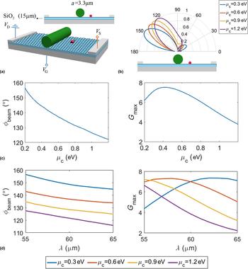
The schematic of the design is depicted in Fig. 3(a). The microwire antenna and the quantum emitter are deposited on a graphene sheet separated from a silver back mirror by silica spacer layer. The spacer layer thickness is chosen as 15 µm in order to achieve enhanced light interaction with the graphene layer. The microwire antenna radius is chosen as a = 3.3 μm and the lateral distance between microwire antenna and quantum dot centers is set as 22 µm. The H-plane radiation pattern corresponding to this design is shown in Fig. 3(b) for different chemical potentials chosen in experimentally accessible range.[Reference Efetov and Kim39] As it can be seen, the subwavelength microwire antenna leads to a directive beam that can be tuned by changing the chemical potential of the graphene via electrostatic gating. Increasing the chemical potential of graphene makes it closer to behave as a metal, as such the trend of beaming angle in radiation pattern is similar to that in the ITO-integrated antenna system. The beaming angle and the maximum gain of the antenna are shown in Fig. 3(c) as a function of graphene chemical potential. According to the results, the beaming angle can be tuned within an angular range of 30° while attaining a reasonably large gain. In this case, the steering range is limited by the achievable range for chemical potential of the graphene.
(a) The schematic of the graphene-integrated design for electrical tuning of the radiation of a wire antenna in the FIR regime. (b) Radiation pattern of the antenna for different chemical potentials of graphene. (c) Beam angle and the maximum gain of the antenna as a function of graphene chemical potential. (d) Angular dispersion and gain variations of the antenna system in a bandwidth of 10 µm.
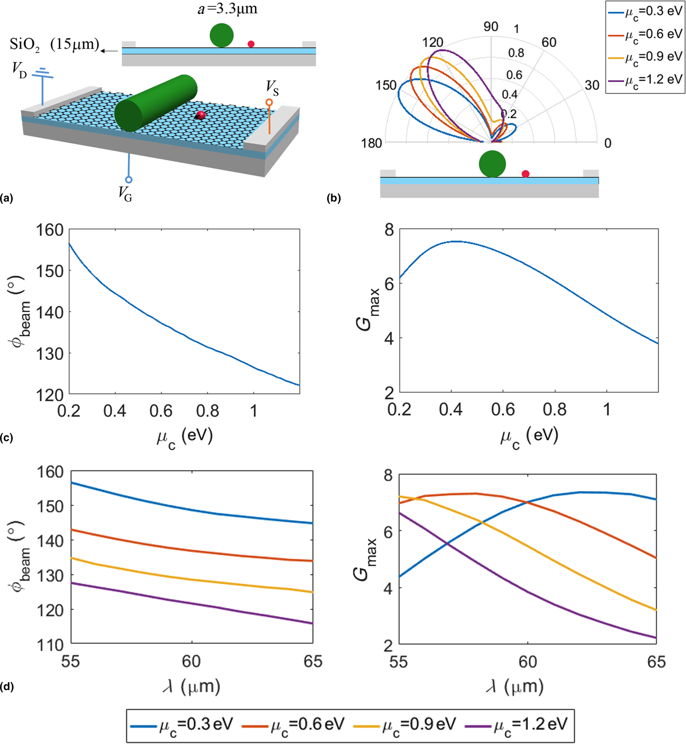
Similar to the ITO-based antenna platform, the angular dispersion is caused here due to the variation of graphene conductivity with the wavelength. The angular dispersion and gain variations of this antenna system are shown in Fig. 3(d) for different chemical potentials of graphene in a bandwidth of 10 µm. As it can be seen, the angular divergence is around 12° in this bandwidth and the gain peak is shifted to shorter wavelengths by increasing the chemical potential.
Conclusions
Substrate-supported nanowire antenna platforms consisted of a nanowire coupled to a dipole emitter were investigated. A robust semi-analytical framework was developed by employing multipole expansion, which offers a great advantage in terms of computational efficiency. This requires complex treatment of different coordinate systems belonging to a cylindrical scatterer, a planar interface, and a spherical source. The method was subsequently used to design and optimize antenna systems with subwavelength footprints capable of directional radiation and real-time tunability in different frequency bands of visible, NIR, and FIR. It was shown that integration of nanoactuators, transparent conducting oxides, and graphene into the substrate platform can be used to achieve this purpose. Unlike the majority of the previous studies, which rely on the excitation of higher order multipoles in the nanowires, the key behind the directive radiation here is the interference effects due to the substrate as well as the asymmetry introduced by the nanowire and induced multipoles. The tunability is achieved by changing the optical path between multipoles and their images into the ground plane. The angular dispersion and gain variations of each antenna system were studied in relatively narrow bandwidths associated with the emission of quantum dots. The correctness of the results and the validity of the developed semi-analytical framework were comprehensively verified by comparison with full-wave simulations.
Supplementary material
The supplementary material for this article can be found at https://doi.org/10.1557/mrc.2018.46
Acknowledgments
The authors would like to acknowledge the supports from US Air Force Office of Scientific Research (AFOSR) FA9550-14-1-0349, US Army Research Office W911NF-15-1-0138, and Defense Advanced Research Projects Agency (DARPA) N00014-14-1-0850.