Individual piezotronic devices
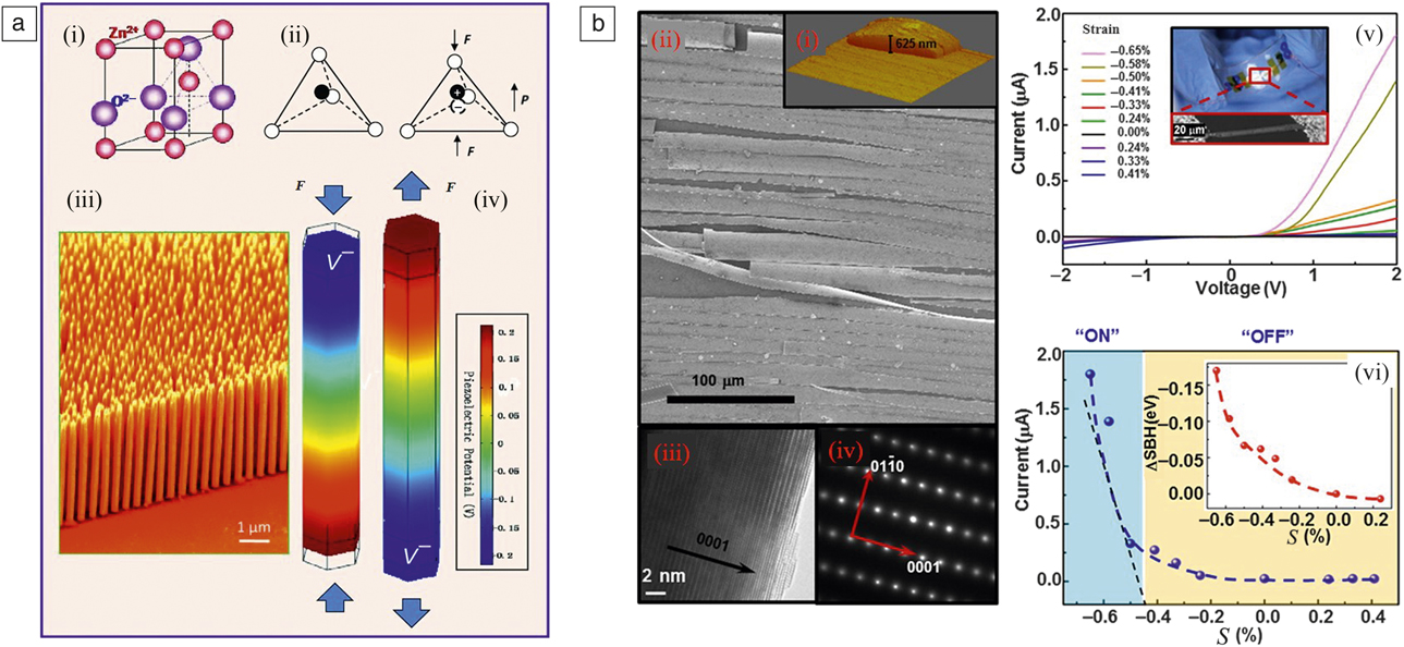
The concept of piezotronics was first introduced more than a decade ago.Reference Wang, Zhou, Song, Liu, Xu and Wang1–Reference Zhou, Gu, Fei, Mai, Gao, Yang, Bao and Wang5 The field was established based on the use of semiconductor crystals that lack inversion symmetry. ZnO is a good example of such a material. It has a wurtzite crystal structure that is noncentrosymmetric, where Zn2+ cations and O2– anions are tetrahedrally coordinated within the lattice. Figure 1a shows an array of ZnO nanowires (NWs) and a piezoelectric potential induced by a mechanical stimulus. By applying stress along the c-axis of the NW, the centers of positive and negative charges can be efficiently displaced relative to each other to form dipole moments, exhibiting a strong piezoelectric potential.Reference Wang6–Reference Wang8 This piezoelectric potential can act as a virtual gate to control carrier transport.
(a) The fundamental principle of piezotronics. (i) Crystal structure of wurtzite ZnO. (ii) The centers of positive and negative charges displaced under the stress. (iii) Scanning electron microscope (SEM) image of aligned ZnO nanowire arrays. (iv) Calculated piezoelectric potential distribution under an axial strain. (b) GaN nanobelt-based strain-gated piezotronic logic devices. (i) GaN nanobelts with thickness of ∼625 nm. (ii) SEM image of GaN nanobelts. (iii) High-resolution transmission electron microscope image and (iv) selected-area electron diffraction pattern. These images show that the GaN nanobelt has single crystallinity with the c-axis parallel to the longitudinal direction. (v) Current–voltage characteristics under different strains. The tensile/compressive strain induced by bending the substrate changes the Schottky barrier height (SBH) to tune the current through the metal–semiconductor–metal structure. The inset is (upper) an optical image and (lower) a digital image of a GaN nanobelt-based piezotronic transistor. (vi) Current–strain characteristics at 2 V bias. The threshold gate strain is determined to be –0.43% by the intersection of the tangent of current–strain curve with the x-axis. The relationship between the SBH change and strain is plotted in the inset. (a) Reprinted with permission from References Reference Wang6 and Reference Gao, Zhou, Gu, Fei, Hao, Bao and Wang7. © 2012 Wiley and 2009 AIP Publishing, respectively. (b) Reprinted with permission from Reference Reference Yu, Wu, Ding and Wang9. © 2013 American Chemical Society. Note: F, applied force; V, potential; P, polarization; S, strain.

In addition to ZnO, a number of II–VI and III–V wurtzite-structured piezoelectric semiconductor materials such as GaN,Reference Yu, Wu, Ding and Wang9,Reference Zhou, Hinchet, Yang, Ardila, Songmuang, Zhang, Zhang, Han, Pradel, Montes, Mouis and Wang10 InN,Reference Ku, Huang, Wang, Fang and Liu11 CdS,Reference Lin, Song, Ding, Liu and Wang12 and CdSeReference Zhou, Han, Rai, Zhang, Ding, Pan, Zhang, Zhou and Wang13 NWs have also demonstrated potential in the field of piezotronics. In the III–V family, GaN is a more extensively studied third-generation semiconductor with wide applications in solid-state lighting and displays, data storage, and power devices. Discussions regarding distinctions between piezoresistive and piezotronic effects and their contributions have been a matter of debate for some time.
However, we have evidence regarding the validity of a piezotronic concept. For example, in a ∼1-μm-long c-plane GaN NW, µN-range normal compressive forces induced piezoelectric charges to change the Schottky barrier height (SBH) and thus modulate the current injected by the tip of conductive atomic force microscope.Reference Zhao, Pu, Han, Du, Li, Jiang, Hu and Wang14 However, a similar modulation could not be observed in a nonpolar m-plane ( $1\bar 100$) GaN NW under a normal compressive force.Reference Zhao, Pu, Han, Du, Li, Jiang, Hu and Wang14 Such a comparison reveals that the piezotronic effect, rather than the piezoresistive effect, dominates the carrier-transport modulations.
Liu et al. systematically investigated the effect of carrier concentration on piezoelectric nanogenerators (PENGs) that used GaN NWs.Reference Wang, Liao, Ku, Li, Chen, Tu and Liu15 With increasing carrier concentration from 1.10 × 1017 cm–3 (undoped) to 5.63 × 1018 cm–3 (doped), the output current of PENGs gradually reached a maximum value of 50 nA, which was attributed to the reduction in the interior resistance. With a further increase in the carrier concentration to 1.53 × 1019 cm–3, the carrier screening effect on the piezoelectric potential became dominant and resulted in a significant reduction of the output current.Reference Wang, Liao, Ku, Li, Chen, Tu and Liu15
Piezotronics provides a direct interface between micro-/nanoelectronic devices and mechanical stimuli. Wang et al. fabricated strain-gated transistors (SGTs) based on GaN nanobelts (Figure 1b).Reference Yu, Wu, Ding and Wang9 In this configuration, the source-drain current decreases as the gate strain increases for which a threshold gate strain >0.4% and a large ON-OFF ratio of nearly 100 were observed. Thus far, piezotronic logic operations such as NOT, AND, OR, NAND, NOR, and XOR have been achieved using these GaN SGTs.Reference Yu, Wu, Ding and Wang9
Carrier mobility degradation due to scattering by dopant centers is a significant problem for one-dimensional (1D) piezotronic devices. One of the possible solutions for reducing such scattering is to resort to heterojunctioning. For example, lateral AlGaN/AlN/GaN microwires (MWs), which were synthesized by metal–organic chemical vapor deposition, are presented in Figure 2.Reference Wang, Yu, Jiang, Hu, Wu, Ding, Peng, Li and Wang16 In this case, the spontaneous piezoelectric polarization bends the energy bands at the heterojunction interface to form a high-density heterojunction electron gas (HEG), which is localized at the interface and spatially separated from the bulk ionized impurities. Thus, AlGaN/AlN/GaN MWs have a higher electron mobility and lower resistance than GaN MWs. Consequently, when a compressive stress is applied to the AlGaN/AlN/GaN MW, the output current is remarkably increased. At temperatures below room temperature, the piezotronic modulation became more significant. The self-consistent calculations reveal that under compressive/tensile stress, the piezoelectric charges deepen/lift the triangular potential well at the interface to increase/decrease the HEG density. This piezotronic modulation provides an extra degree of freedom to design high mobility electronic transistors (HEMTs) or micro-/nanoelectromechanical systems, allowing for strain-modulated AlGaN/GaN HEMTs and metal oxide semiconductor HEMTs.Reference Liu, Jiang, Huang, Du, Zhao, Jing, Li, Han, Sun, Pu, Zhai and Hu17,Reference Jiang, Liu, Du, Huang, Liu, Zhao, Li, Pu, Zhai, Hu and Lin Wang18
Piezotronic effect modulated heterojunction electron gas (HEG) in an AlGaN/AlN/GaN heterostructure microwire.Reference Wang, Yu, Jiang, Hu, Wu, Ding, Peng, Li and Wang16 (a) High-angle annular dark-field scanning transmission electron microscope image of AlGaN/AlN/ GaN heterostructure, which reveals atomically uniform and sharp interfaces. (b) Schematic diagram of the atomic structure. (c) Schematic diagram of the energy band structure. The spontaneous/piezoelectric polarizations bend the energy bands at the AlN/GaN interface to form a HEG. (d) Current–voltage characteristics under different strains, which reveals the conductance decreases/increases with the applied tensile compressive strain. The tensile/compressive strain induces the piezoelectric charges to lift/deepen the triangular potential well to decrease/increase the HEG density. Note: P lm, piezoelectric polarizations induced by the lattice mismatch;  $P_{{\rm{sp}}}^{{\rm{AlGaN}}}$, spontaneous polarization of AlGaN;
 $P_{{\rm{sp}}}^{{\rm{GaN}}}$, the spontaneous polarization of GaN;
 $E_{\rm{C}}^{}$, conduction band;
 $E_{\rm{F}}^{}$, Fermi level;
 $S_{\rm{C}}^{}$, compressive strain;
 $S_{\rm{T}}^{}$, tensile strain; T, temperature.

Other materials have also been used for developing piezotronic devices. Metalloids, such as Te, have been successfully used in this regard. Kou et al.Reference Kou, Zhang, Liu, Zhang, Liu and Zhai19 fabricated a nanoforce sensor based on a single Te NW that demonstrated a response to forces as small as ∼5 nN. Wu et al. reported the piezotronic effect in a 1D van der Waals solid of Te nanobelts.Reference Gao, Wang, Wang and Wu20 Another material that has been reported for developing piezotronic strain sensors is ZnSnO3, which has a rhombohedral structure (R3c) that exhibits relatively large polarization along the c-axis as compared to ZnO. Advantageously, a fabricated piezotronic strain sensor based on the ZnSnO3 NW demonstrated high ON/OFF ratios of 587 and gauge factor of 3740. The value of the gauge factor is three times higher than that for ZnO NWs.Reference Wu, Chen, Zhang, Chen, Yang, Hu, He and Wang21
These studies on 1D piezotronic materials have expanded our understanding of carrier transport under the piezoelectric field, provided the needed vision for piezotronic materials, and exhibited great potential for future electronic devices beyond Moore’s Law, which refers to the density of devices doubling every 18 months. However, at the end of Moore’s Law, diversity and multifunctionality add more developing dimensions for electronic devices to extend beyond Moore’s Law.Reference Wang6
Large-scale piezotronic arrays
Integrating nanodevices into a functional system is a milestone for electronic devices. The rapid advancement in nanotechnology makes it possible to fabricate integrated piezotronic circuits. The first large-array circuit integration of piezotronic transistors was reported in 2013.Reference Wu, Wen and Wang22 Wang et al. fabricated a 92 × 92 strain-gated vertical piezotronic transistor (SGVPT) array and realized active and adaptive tactile imaging by combining the patterned in-place growth of vertically aligned ZnO NWs and state-of-the-art microfabrication techniques. This large-scale SGVPT array was sandwiched between the top and bottom transparent indium tin oxide (ITO) electrodes (Figure 3a).Reference Wu, Wen and Wang22 Au thin films were inserted between ZnO surfaces and ITO electrodes, and an Au/ZnO Schottky contact was used as the piezotronic gate. These electrodes took the orthogonal configuration and were individually, or in clusters, addressable.
Integrated piezotronic circuit. (a) Schematic illustration of a strain-gated vertical piezotronic transistor (SGVPT) array. (i) The device structure consists of a ZnO nanowire (NW) array and addressable top/down electrodes. The red/blue color represents the positive/negative piezopotential under downward pressure. (ii) Equivalent circuit diagram. (b) Current response under different applied pressures. Bottom left inset illustrates that when the piezopotential is under a downward pressure, the Schottky barrier height increases, which results in a decreasing current. The dependence of current variations on the pressure are plotted in top right inset, which indicates the current variations saturating at a pressure above ∼30 kPa. (c) Pressure visualization. Six normal stresses, indexed from 1 to 6, were applied on a SGVPT array, and their spatial distribution follows the letter A. The contour of the response current exhibits the shape of the “written” letter A. Reprinted with permission from Reference Reference Wu, Wen and Wang22. © 2013 AAAS. Note:  $E_{{\rm{F}},{\rm{top}}}^{}$,Fermi level at the interface between ZnO NWs and top electrode;
 $E_{{\rm{F}},{\rm{ZnO}}}^{}$, Fermi level in ZnO; E C, conduction band;
 $E_{\rm{V}}^{}$, valance band;
 $E_{{\rm{piezo}}}^{}$, piezoelectrical polarization; I, current; S, strain.

Figure 3b shows the output current of an individual tactile pixel (taxel) under 1 V bias and different pressures for this circuit. According to the schematic band diagram (lower left inset in Figure 3b), the normal pressure induced negative piezoelectric charge at the top Au/ZnO contact to raise the SBH and decreased the output current. The sensitivity for pressure sensing was estimated to be approximately 2 µS kPa–1 and the sensing ranged from a few kPa to ∼30 kPa. The response time in the subsecond range can be obtained for such circuits. These systems can be practically used in current electronic devices.
As a demonstration, a group of six normal pressure stimuli was applied to the SGVPT array and the spatial distribution followed the letter “A” (outlined by the white dashed lines in Figure 3c). The contour plot of the output current exhibits a clear spatial distribution matched to the six applied stresses that are indexed from 1 to 6 in the figure. The spatial resolution of pressure sensing can indeed exceed high dot-per-inch (dpi) resolutions. It has been shown that by assembling hexagonal ZnO nanoplatelets into an ordered array, the spatial resolution of the pressure sensors was increased to 12,700 dpi.Reference Liu, Wang, Feng, Wang, Xu, Bai, Qin and Wang23 Spatial pressure visualization and recording can also be simultaneously realized. Han et al. successfully integrated WO3 electrochromic device films and a ZnO-NW-matrix pressure sensor for this purpose.Reference Han, Du, Chen, Wang, Zhang, Li, Li, Peng, Pan and Wang24
Such examples are obvious evidence that large-scale piezotronics arrays offer great potential for implementation in applications such as human–machine interfacing, robotics, and biomedical devices.
Future perspectives
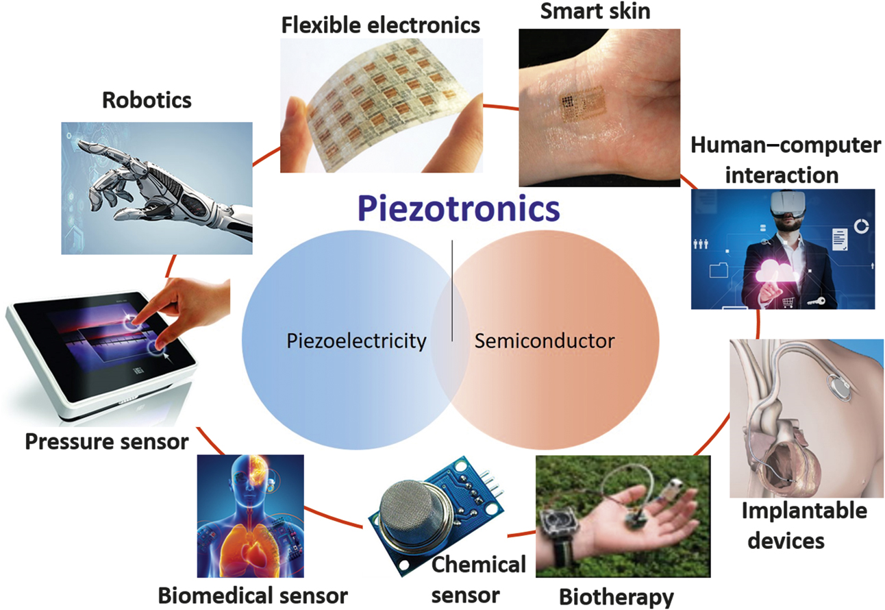
Since the discovery of piezotronics, 1D ZnO nanostructures with polar c-axis orientation have been extensively investigated for a wide range of piezotronic applications, including SGTs,Reference Wang, Zhou, Song, Liu, Xu and Wang1,Reference Zhou, Gu, Fei, Mai, Gao, Yang, Bao and Wang5,Reference Wu, Wei and Wang25 programmable resistive memories,Reference Wu and Wang26 and piezoelectric chemical sensors (Figure 4).Reference Niu, Hu, Wen, Zhou, Zhang, Lin, Wang and Wang27,Reference Lao, Kuang, Wang, Park and Deng28 Piezotronic effects, and their applications for novel devices, have been reported in biomedical sensors (Figure 4)Reference Cao, Cao, Guo, Li, Jie, Wang and Wang29 and logic circuits.Reference Yu, Wu, Ding and Wang9 Other than ZnO, III–V piezoelectric semiconductor materials also offer great promise for piezotronics. Axial orientation dependence of piezotronics (i.e., c-axial, m-axial, and a-axial 1D nanostructures) has also been explored.Reference Wang, Peng, Pan and Wang30 Recently, new material candidates, including metalloids, have been reported for developing piezotronic devices.Reference Kou, Zhang, Liu, Zhang, Liu and Zhai19–Reference Wu, Chen, Zhang, Chen, Yang, Hu, He and Wang21
Schematic diagram showing future prospects of piezotronics, which is coupling between piezoelectric and semiconducting properties of piezoelectric semiconductors. This is anticipated to lead to many significant novel applications of multifunctional sensing systems, human–electronics interfacing, microelectromechanical systems, and many other areas.

Based on high sensitivity SGTs, piezotronic logic devices can convert a mechanical stimulus to a digital signal for logical computation.Reference Yu, Wu, Ding and Wang9,Reference Wu, Wei and Wang25 Since piezotronic transistors can be applied to strain sensors, signal comparators, and amplifiers, flexible and low-power piezotronic analog-to-digital converters based on SGTs have been reported, which can be used for converting external applied strains to logic bits by using circuit architectures formed by various networks composed of SGTs and resistors.Reference Nie, Hu, Li and Zhang31 Another application of the piezotronic effect has been reported in the modulation of the low-dimensional heterojunction electron gas in high-electron-mobility transistors.Reference Wang, Yu, Jiang, Hu, Wu, Ding, Peng, Li and Wang16 The piezotronic effect can be employed to modulate the physical properties of the electron gas near heterojunctions and tune/control the electric transport process of carriers across the heterojunctions. Moreover, taxel-addressable pressure/force-sensor matrices for active and adaptive tactile sensing have recently been reported.Reference Wu, Wen and Wang22–Reference Han, Du, Chen, Wang, Zhang, Li, Li, Peng, Pan and Wang24 There are also many other unexplored areas in which piezotronic devices can be efficiently employed.
Reliability is a significant issue for future piezotronic devices. In situ transmission electron microscope measurements reveal that single-crystal ZnO NWs can endure mechanical deformation of no more than 1.81% for 1010 cycles without exhibiting mechanical failure or defects.Reference Gao, Ding, Lin, Hao and Wang32 While designing piezotronic devices, the appropriate strain range should be chosen to avoid wearing or tearing of piezoelectric semiconductors. The mechanical degradation of metal electrodes is also expected to be a significant hindrance for the dynamic stability of the piezotronic devices. New electrode materials (e.g., carbon nanotubes,Reference Sekitani, Noguchi, Hata, Fukushima, Aida and Someya33 conducting polymer,Reference Vosgueritchian, Lipomi and Bao34 or grapheneReference Kim, Zhao, Jang, Lee, Kim, Kim, Ahn, Kim, Choi and Hong35) or flexible electrode structures (e.g., buckled, arc-shaped interconnecting structuresReference Rogers, Someya and Huang36) are expected to improve the mechanical stability. In addition, moisture absorption or heat failure should be considered for some special piezotronic devices that are operated under extreme conditions.
The piezotronic field is advancing quickly with the emergence of novel materials, multifunctional micro-/nanoelectronic devices, and high integration of piezotronic circuits with promising applications in diverse areas such as human–machine interfacing, robotics, implantable sensors, flexible electronics, and smart skin (Figure 4).

Weiguo Hu is a principal investigator at the Beijing Institute of Nanoenergy and Nanosystems, Chinese Academy of Sciences (CAS), China. He received his PhD degree from the Institute of Semiconductors, CAS, in 2007. His research focuses on gallium nitride-based piezotronic/piezo-phototronic devices and wearable self-powered nanosystems. He has authored more than 60 peer-reviewed journal articles in these fields. Hu can be reached by email at huweiguo@binn.cas.cn.

Kourosh Kalantar-Zadeh is a professor in the School of Chemical Engineering at the University of New South Wales, Australia. Prior to this, he was a professor of electronic engineering at the RMIT University, Australia. He has co-authored nearly 400 research articles and reviews. He is a member of the editorial boards of various journals, including Applied Materials Today, ACS Applied Nano Materials, ACS Sensors, Advanced Materials Technologies, and Nano-Micro Letters. His awards include the 2017 IEEE Sensor Council Achievement and 2018 ACS Advances in Measurement Science Lectureship Awards. Kalantar-Zadeh can be reached by email at k.kalantar-zadeh@unsw.edu.au.

Kapil Gupta is a postdoctoral fellow in the Department of Materials Science and Engineering at National Cheng Kung University, Taiwan. He received his PhD degree in physics from the Indian Institute of Technology Madras, India, in 2015. His current research focuses on nonstoichiometric perovskite oxides, nanomaterials, transmission electron microscopy, piezotronics, piezo-phototronics, and nanogenerators. Gupta can be reached by email at kapilmsrc@gmail.com.

Chuan-Pu Liu is a distinguished professor in the Department of Materials Science and Engineering at National Cheng Kung University, Taiwan. He received his PhD degree from the Department of Materials Science and Metallurgy at the University of Cambridge, UK, in 1998. He conducted postdoctoral research in the Materials Research Laboratory at the University of Illinois at Urbana-Champaign. He has published approximately 200 journal papers. His current research interests include semiconductor nanomaterials, transmission electron microscope atomic-scale imaging, nanodevices, and piezotronic and thermoelectric devices, lithium-ion batteries, and gas and chemical sensors. Liu can be reached by email at cpliu@mail.ncku.edu.tw.