I. INTRODUCTION
The internet of things (IoT), ubiquitous electronics and related technology developments will require an enormous growth in wireless devices [Reference Evans1–Reference Nathan3]. This is because of the tremendous spread of electronic circuits and components in the everyday objects for applications like monitoring, labeling, logistics, and so forth. IoT implies having interconnected objects able to collect data by interacting with the environment and to transfer them to internet. In this scenario, the development and the design of miniaturized, low-cost, high efficient, autonomous, and highly integrated technologies and solutions play a fundamental role.
For stand-alone and wirelessly connected devices, like the tags of radio frequency identification (RFID) systems and the nodes of wireless sensor networks (WSNs), autonomy is a crucial aspect [Reference Kim, Mariotti, Alimenti, Mezzanotte, Georgiadis, Collado, Roselli and Tentzeris4–Reference Vyas, Cook, Kawahara and Tentzeris6]. In this scenario, we think that wireless power transfer (WPT) [Reference Roselli, Alimenti, Orecchini, Mariotti, Mezzanotte and Virili7–Reference Popovic12] and energy harvesting (EH) [Reference Roselli, Alimenti, Orecchini, Mariotti, Mezzanotte and Virili7, Reference Beeby and White13–Reference Guenda, Santana, Collado, Niotaki, Carvalho and Georgiadis16] are the most promising technologies to cope with autonomy: WPT allows electronic devices to be wirelessly supplied by electromagnetic (EM) energy generated by ad-hoc sources; EH, in turn, allows energy from the environment to be recovered to power supply electronics. Recent studies testify also systems able to exploit mixed energy sources, like solar-EM [Reference Collado and Georgiadis17], and thermal-EM [Reference Virili, Georgiadis, Niotaki, Collado, Alimenti, Mezzanotte, Roselli and Carvalho18], and their integration for several applications [Reference Collado and Georgiadis17–Reference Lemey, Declercq and Rogier20] such as space and wearable structures.
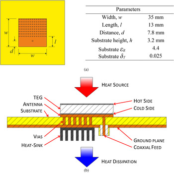
According to this evolution, after a brief description of the WPT and EH techniques, this paper resumes the design of a quarter-wavelength patch antenna integrated with a thermo-electric generator (TEG) [Reference Virili, Georgiadis, Niotaki, Collado, Alimenti, Mezzanotte, Roselli and Carvalho18] (see Fig. 1(b)) working as a transducer able to convert thermal energy to dc. The antenna operates in the industrial, scientific, and medical (ISM) 2.4–2.5 GHz frequency band. Then, the design of a rectifier with improved performance and working at the same frequency of the antenna is described. In particular, the antenna combined with the rectifier can be used to perform EM EH, while the TEG is used to perform the thermal EH and to increase the rectifier performance by biasing it. This ends up in a single system with improved energy conversion efficiency, and thus in increasing the autonomy and performance of wireless systems such as passive RFID nodes, wireless sensors, and so on. The double positive effect of increasing the overall amount of energy harvested, thermal, and EM, and of improving the conversion efficiency in the operating low radio frequency (RF) power conditions is evaluated.
Top view of the antenna layout and its dimensions (a) (© 2014 IEEE. Reprinted, with permission, from [Reference Virili, Georgiadis, Niotaki, Collado, Alimenti, Mezzanotte, Roselli and Carvalho18]) and section of the antenna-TEG structure with thermal flux (b).

II. WPT AND EH
EH consists of collecting energy from several environmental sources (EM, thermal, solar, wind, etc.) [Reference Vullers, Schaijk, Visser, Penders and Hoof14] and converting it to electric energy. This energy can be used to power appliances, making them independent from the power grid and batteries.
A) EM WPT and EH
The EM EH is often combined with WPT and the interest for them is increasing, thanks to the proliferation of RFIDs and WSNs [Reference Roselli, Alimenti, Orecchini, Mariotti, Mezzanotte and Virili7–Reference Guenda, Santana, Collado, Niotaki, Carvalho and Georgiadis16]. In principle, the main difference between the pure EM EH and the harvesting supported by radiative WPT is the energy source. Pure EH exploits energy already present, and usually wasted, in the environment (think, for instance to the so called “electro-smog” [Reference Pinuela, Mitcheson and Lucyszyn21]). WPT supported harvesting, instead, implies that an ad-hoc source (recently called also “energy shower” [Reference Costanzo22]) is set up to power supply wirelessly a device or a group of them. WPT, in turn, can be developed to exploit near-fields or far-fields [Reference Garnica, Chinga and Jenshan10, Reference Valenta and Durgin11]; in both cases, the circuitry used to collect the energy is conceptually the same and makes use of rectennas [Reference Brown, George and Heeman23–Reference Hagerty, Helmbrecht, McCalpin, Zane and Popovic25]: a combination of an antenna and a rectifier optimized to improve the RF-to-dc conversion efficiency.
The rectifiers, the state-of-the-art of which is documented in [Reference Valenta and Durgin11, Reference Boaventura, Collado, Carvalho and Georgiadis26], are key elements of EM EH systems. They convert the RF input power to dc power. It is done by using a non-linearity. For low RF input power, low-threshold devices, such as Schottky diodes, are usually a good choice. Several circuit topologies can be adopted, ranging from the single diode rectifier to the multi-stage ones (the so called charge pumps). The latter ones allow for greater output voltage with the trade-off of reducing the efficiency because of the presence of more non-linear devices. The use of resistance compression networks (RCN) [Reference Han, Leitermann, Jackson, Rivas and Perreault27] has been recently introduced to reduce the rectifier impedance variation, and therefore the mismatching, as a function of the RF input power. Dual-band rectifiers with RCNs have been proposed to exploit the energy of multiple frequency bands [Reference Niotaki, Georgiadis and Collado28].
B) Thermal EH
The thermal energy is available in almost any environment. The thermo-electric energy conversion is based on the use of transducers usually called TEGs, able to generate electricity from a temperature gradient applied to their sides. TEGs can be integrated into autonomous systems, like in the present case, to enhance lifetime and capability of self-powering.
The TEGs rely on the Seebeck effect [Reference Beeby and White13, Reference Vullers, Schaijk, Visser, Penders and Hoof14] that consists of the generation of a voltage by applying a temperature difference across two junctions of two conductive materials with different working functions [Reference Beeby and White13]. The modern TEGs are fabricated exploiting semiconductors, because the Seebeck coefficient of doped semiconductors is larger than the metal ones. Their basic structure, the thermocouples, consists of a n-type and a p-type semiconductor connected electrically in series. A TEG is generally made of several basic structures connected electrically in series but thermally in parallel between two ceramic plates. These plates, at which the temperature gradient is applied, allow the device to be electrically isolated.
III. SYSTEM DESIGN
A) Antenna-TEG
The design of the antenna with the TEG, extensively described in [Reference Virili, Georgiadis, Niotaki, Collado, Alimenti, Mezzanotte, Roselli and Carvalho18], was carried out to obtain an integrated solution providing mixed EH (improved RF and thermal) at the same time. The already proposed solution allows the integration level of the structure to be improved, while fitting the thermal and dimensional constraints introduced by TEG, as reported in [Reference Virili, Georgiadis, Niotaki, Collado, Alimenti, Mezzanotte, Roselli and Carvalho18].
The antenna topology consists of the quarter-wave square patch antenna. The antenna layout and its dimensions, optimized to match the antenna to 50 Ω in the IMS frequency band 2.4–2.5 GHz, are reported in Fig. 1(a) (such as in [Reference Virili, Georgiadis, Niotaki, Collado, Alimenti, Mezzanotte, Roselli and Carvalho18]).
The section of the stacked solution proposed in [Reference Virili, Georgiadis, Niotaki, Collado, Alimenti, Mezzanotte, Roselli and Carvalho18] is shown in Fig 1(b). The TEG is positioned on top of the antenna that provides a mechanical support. The heat source is assumed over the structure and it is directed to the hot side of the TEG. The cold side of the TEG is buried and in direct contact with the copper patch antenna. The through-vias allow the top metal layer of the antenna to be electrically and thermally connected to the ground plane, and therefore also the cold side of the TEG results thermally connected to the ground plane. In this way the ground plane behaves as a heat-sink. A heat-sink can be mounted (as in the present case) in contact with the ground plane to improve the thermal efficiency of the whole structure.
B) Rectifier
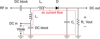
In this work a single-diode rectifier topology has been chosen because it exhibits a better efficiency at low RF input power than multi-stage solutions. However, its efficiency at low power levels is still compromised by the threshold voltage of the diode, even if a low-barrier Schottky diode is chosen as in this case [29]. When a RF signal is applied to the diode, it generates a dc component that provides as a self-biasing voltage, but it is usually not enough to reach the optimum bias-point. An external voltage should be used to bias the diode and thus to improve the RF-to-dc conversion efficiency. Unfortunately this is not available in passive nodes, but in our combined harvester the TEG is just used to provide it.
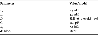
In the proposed configuration shown in Fig. 2, dc blocks have been added to the basic single-diode rectifier schematic to properly bias the diode with the voltage harvested by the TEG. The dc block at the RF input allows the shorting of dc voltage at the antenna to be avoided: the quarter-wave patch antenna, in fact, is a short circuit at dc. The other dc block, between the dc input pin and the ground, allows the diode anode not to be shorted at dc. The inductors, L 1 and L 2, play two roles: the first one is to provide a matching network between the 50 Ω antenna and the rectifier; the second one is to provide a dc path from the dc input to the diode. The complete dc path goes from the TEG (that provides the V BIAS between the dc input and the ground), through L 1, L 2, the diode, and R L (see Fig. 2). The values of C L and R L have been optimized to obtain the best RF-to-dc conversion efficiency. The values of the rectifier components and the diode model are listed in Table 1.
Rectifier schematic with external dc bias voltage adopted to coexist with the TEG.

Components values of the rectifier.

IV. MEASUREMENTS
Two different measurement setups were used to characterize the electromagnetic and the thermal EH performance. Then, the performance of the rectifier, opportunely designed to exploit the harvested energy generated by the TEG, has been measured.
A) EM performance of antenna and TEG
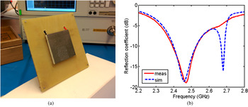
In this section, the results obtained in [Reference Virili, Georgiadis, Niotaki, Collado, Alimenti, Mezzanotte, Roselli and Carvalho18] are summarized. The reflection coefficient and the radiation patterns of the antenna with TEG prototype shown in Fig. 3(a) have been measured exploiting a Vector Network Analyzer (VNA). Figure 3(b) shows the comparison between the measured reflection coefficient and the simulated one: the two curves are below −10 dB and present a maximum relative error of about 0.2 in the operating ISM frequency band. The simulated reflection coefficient exhibits a dip close to 2.7 GHz, introduced by the TEG that is modeled with a lossless high permittivity block as described in [Reference Virili, Georgiadis, Niotaki, Collado, Alimenti, Mezzanotte, Roselli and Carvalho18]. This block introduces a resonance between the two plates of the TEG that, in the real case, is attenuated by the conductive elements inside the TEG, not accounted by the model. For this reason, the measurement exhibits only a slightly hinted dip in correspondence of the simulated one. The simulated radiation efficiency is about 70 % and the measured gain in the direction orthogonal to the antenna plane, is equal to 2.3 dBi. The heat-sink connected to the ground does not significantly affect the antenna EM performance.
Prototype of the antenna with TEG (a) and reflection coefficients (b). Prototype of the antenna with TEG (a) (© 2014 IEEE. Reprinted, with permission, from [Reference Virili, Georgiadis, Niotaki, Collado, Alimenti, Mezzanotte, Roselli and Carvalho18]) and reflection coefficients (b).

B) Thermal performance of antenna and TEG
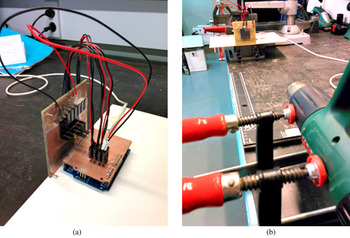
The measurements of the thermal performance have required the use of temperature sensors and a microcontroller with Analog-to-Digital Converters (ADCs) to perform the acquisition and the data processing. The thermal sensors adopted are the LM35 [30]. These sensors present an analog output proportional to their package temperature with an accuracy of ±1 °C. Highly thermally conductive copper packages, (thermal conductivity of the copper being (401 W/m/K), have been realized and mounted on the LM35 sensor to measure the temperature of the structure by putting them in direct contact with the surfaces of interest (the hot and the cold sides of the TEG and the antenna ground). A 100 kΩ load resistor has been soldered at the TEG terminals just for the purpose of its characterization as a Thévenin's source. An Arduino UNO board [31], mounting the microcontroller ATmega328, has been used to acquire and process the temperature sensors signals and the voltage generated by the TEG. The ADCs have a resolution of 10 bits, which corresponds to 1024 values, and to a less significant bit of 1.075 mV, considering an ADCs reference voltage of 1.1 V. The Arduino UNO board with the shield board mountable on it (developed to connect the sensors and the TEG output), and the assembled prototype connected to the acquisition system are shown in Fig. 4(a). Between the board of the acquisition system and the one of the antenna there is an air gap of about 5 mm that ends up in a strong thermal isolation.
Assembled antenna-TEG prototype with acquisitions system (a) and measurement setup (b).

The thermal to dc conversion performance of the stand-alone TEG and the system antenna-TEG has been analyzed for different temperatures. The measurement setup of the system antenna-TEG is shown in Fig. 4(b). A heat-gun, able to generate an air flow with a tunable temperature, was positioned 25 cm far from the devices under test (DUTs): the stand-alone TEG and the system antenna-TEG. The measurements have been performed by varying the temperature of the heat-gun: this means that the nominal temperature in the plots is referred to the heat-gun one, not to that of the air flow at the DUT interface. To improve the performance of the TEG an additional heat-sink was adopted in both cases: it was attached directly to the cold side of the TEG in the case of the stand-alone TEG; while it was attached to the ground plane of the antenna in the case of the system antenna-TEG.
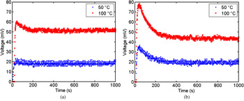
The voltages generated by the TEG in the two cases are plotted in Fig. 5. The measurements have been performed setting the heat-gun temperature to 50 and 100 °C. They show a transient and a steady-state behavior; this happens because, at the starting instant, the DUT is at ambient temperature. The maximum voltage is obtained during the transient because the hot side temperature increases faster than the cold side one, due to the prominent capacitive behavior of the whole structure from a thermal point of view. After the transient, up to about 250 s, the structure reaches a thermal equilibrium and the generated voltage exhibits, in both cases, a constant behavior. It is worth noticing that the stand alone system reaches a regime output voltage slightly higher and a peak voltage lower than the whole TEG-antenna structure, this is much likely due to the variations of thermal resistance introduced by the antenna layers. The same measurements have been performed also without the heat-sink: their comparison highlights an improvement of the generated voltage in the steady-state of about 1.5 times for both 50 and 100 °C in presence of the heat-sink.
Voltage generated by the TEG versus time at two different heat-gun temperatures: (a) stand-alone TEG; (b) antenna-TEG system.

C) Rectifier performance
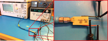
A measurement campaign has been carried out to estimate the conversion performance of the rectifier as a function of the RF input power and the dc voltage used to polarize the diode. A VNA has been used to measure the reflection coefficients. The measurement setup adopted to measure the RF-to-dc conversion performance (consisting of a signal generator, a power supply, and a multi-meter) and the DUT are shown in Fig. 6. To improve the quality of the measurements, the cable losses have been compensated.
Measurement setup with zoom on the DUT.

The rectified dc output voltage at the load resistance (see Fig. 2) has been measured by varying the RF input power, P RF_IN , and the dc voltage, V BIAS, used to polarize the diode at dc input pin (see Fig. 2). The output power, P DC_OUT , and, therefore, the efficiency, η, have been computed measuring the dc voltage at the load resistance, R L , equal to 2.2 kΩ. V BIAS has been varied in agreement with the voltage generated by the TEG (see Fig. 5).
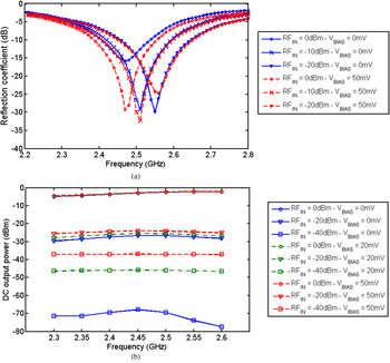
The frequency behavior of the rectifier is shown in Figs 7(a) and 7(b). Figure 7(a) shows the reflection coefficient measured with the VNA by varying the RF input power and the polarization voltage, V BIAS . The dip of the reflection coefficient, and thus the optimum matching point, shifts to higher frequencies varying the RF input power. Nevertheless, the use of a polarization voltage allows the matching to be generally increased: the reflection coefficients curves obtained for a polarization voltage of 50 mV reach lower values for an RF input power of 0 and −10 dBm in comparison with those ones obtained for a polarization voltage of 0 mV. The output power versus frequency assuming RF input power and diode polarization voltage as variable parameters is shown Fig. 8(b). The maximum output power value slightly shifts to higher frequency when the RF input power increases, in particular from 2.45 GHz for P RF_IN equal to −40 dBm to 2.55 GHz for P RF_IN equal to 0 dBm. This frequency behavior is related to the variation of the diode impedance, and therefore the overall rectifier impedance, as a function of the input power. Increasing the RF input power, the measured output power curves, obtained for different values of V BIAS , trends to converge while a difference of more than 30 dB between the 0 and 50 mV bias cases is clearly detected, confirming the potential of the proposed approach at RF low power regimes.
Measured reflection coefficient (a) and output power (b) versus frequency and assuming the input RF power and the polarization voltage as variable parameters.

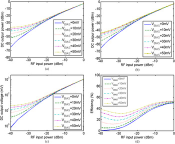
Rectifier measurements: (a) overall dc output power, P DC _ OUT (see equation (1)); (b) output power related to the RF-to-dc conversion only, P DC _ OUT _ R2D (see equation (2)); (c) dc output voltage; (d) efficiency (see equation (3)). The measurements are functions of the RF input power at 2.45 GHz.

The output power, P DC_OUT , in small-signal conditions can be approximated as the sum of two contributions as follows:
 $$P_{DC\_OUT} = P_{DC\_OUT\_BIAS} + P_{DC\_OUT\_R2D},$$
where P DC _ OUT_BIAS is the power related to the polarization voltage applied to the diode measured in absence of RF input power; and P DC _ OUT _ R2D is the power obtained from the RF-to-dc (R2D) conversion. In this way, the RF-to-dc conversion power contribution can be computed knowing P DC _ OUT and P DC _ OUT _ BIAS as a function of the polarization voltage as follows:
 $$P_{DC\_OUT\_R2D} = P_{DC\_OUT} - P_{DC\_OUT\_BIAS}.$$
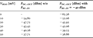
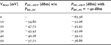
Figure 8 shows the overall output power P DC_OUT (Fig. 8(a)), the RF-to-dc conversion contribution P DC_OUT_R2D (Fig. 8(b)), and the output voltage (Fig. 8(c)). The overall output power P DC_OUT , for RF input power lower than about −20 dBm, increases with the V BIAS , and it is close to the power provided by the polarization voltage for very low values of P RF_IN (see Table 2); the curves converge asymptotically by increasing the RF input power P RF_IN , as expected. Also RF-to-dc converted power, P DC_OUT_R2D , curves converge increasing the RF input power P RF_IN . It was expected and it is due to the increasing capacity of the RF signal to self-bias the diode, the efficiency of which is not influenced by the biasing signal any longer. Anyway, from Fig. 8(b) it can be noticed that the RF-to-dc power contribution, P DC_OUT_R2D , increases by increasing the polarization voltage level for low RF input power. This means that, polarizing the diode, a better conversion efficiency is obtained. It must be noticed, moreover, that the RF-to-dc contribution is dominant for high RF input power.
Dc output power without RF input power and with RF input power equal to −40 dBm at 2.45 GHz.
The efficiency of the whole system can be defined as:
 $$\eta _{RF + DC} = \displaystyle{{P_{DC\_OUT}} \over {\left( {P_{RF\_IN} + P_{DC\_IN}} \right)}},$$
where P RF _ IN is the RF input power, P DC _ IN is the biasing input power, and P DC _ OUT is the whole output power due to polarization voltage and to the RF-to-dc converted power. This efficiency is shown in Fig. 8(d) and takes into account all the power contributions involved. For a polarization voltage equal to zero, the efficiency is about 22% for a P RF _ IN of −20 dBm and 41% for a P RF _ IN of −10 dBm, in agreement with the state-of-art in [Reference Valenta and Durgin11]. The efficiency is improved by the polarization voltage at low P RF _ IN and the curves converge to almost a same value for higher P RF _ IN , as expected. The efficiency value increases, in the best case, from 0.3% up to 38% for a P RF _ IN of −40 dBm and a V BIAS of 50 mV, resulting in the best measured efficiency increment. Reducing the P RF _ IN while keeping constant V BIAS (and thus P DC _ IN ) the efficiency trends to be constant; this constant value is actually the ratio P DC _ OUT /PDC _ IN that can be seen as the “dc” efficiency of the rectifier, i.e. its capacity to transfer the electric power, harvested by the TEG and used to bias the diode, to the load.
Three main operating regions, depending on the power contributions as a function of the input power, can be identified: below −30 dBm the main contribution to the output power is due to the TEG presence (such as demonstrated from the values in Table 2); roughly between −30 and−20 dBm there is a transition region in which the contribution of the RF-to-dc conversion increases significantly due to the better conversion efficiency of the biased diode; and above −20 dBm where the main contribution is due to the RF-to-dc conversion provided by the rectifier that, being also self-biased by the RF is not too sensitive to the dc provided by the TEG.
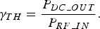
To underline the advantage of the proposed solution incorporating thermal harvesting, we dare define a new parameter:
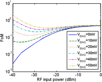
 $$\gamma _{TH} = \displaystyle{{P_{DC\_OUT}} \over {P_{RF\_IN}}}.$$
This parameter can be seen as a sort of economical quality factor of the system that accounts only for those power contributions that have an economical relevance: a value in output and a cost in input. So, because all the output dc power is valuable, while only the RF input power is costly in a WPT system (thermal energy is assumed for free); γ TH can be seen as a figure of merit (FoM) for this kind of mixed harvesting systems. Note that this FoM is 1 (or 0 dB) when all the cost paid at the input is recovered as value at the output.
In case of conventional rectifier of course, due to the conversion efficiency, clearly not ideal, this FoM γ TH is always <1 and, multiplied by 100, corresponds to the efficiency of the rectifier. In our case, due to the thermal energy harvested and its dual fold exploitation as an additional free energy source and as a means to increase the efficiency of the rectifier, γ TH can go even far beyond 1 (see Fig. 9) at low RF input power. Note that γ TH greater than unit means that the actual output dc power is greater than what it would be if it were obtained by harvesting only EM energy and converted to dc by using an ideal rectifier with 100% of efficiency.
γ TH = P DC _ OUT /PRF _ IN in logarithmic scale as a way to emphasize the economic advantage of exploiting the free thermal energy and to provide a FoM to compare the performance of mixed (EM plus any other form of energy environmentally available for free) energy harvesters.

V. CONCLUSIONS
The design of an integrated, dual energy harvester for wireless autonomous nodes is presented in this paper. It consists of the integration of a TEG module with an antenna and a rectifier. Several measurement setups have been built to investigate the EM, the thermal, and the RF-to-dc conversion behavior of the system. The antenna and the rectifier operate in the ISM 2.4–2.5 GHz; the former is used to collect EM energy and the latter is necessary to convert the harvested EM energy into dc one. The antenna measurements show that the reflection coefficient is below −10 dB in the overall operating frequency band and its gain, measured in the E- and H-plane is 2.3 dBi in the direction orthogonal to the antenna plane. The TEG, in turn, is used to harvest thermal energy and it is able to generate about 20 and 50 mV for a heat air flux at 50 and 100 °C, respectively. The rectifier measurements show an improvement of the RF-to-dc power conversion for low RF input power, obtained by polarizing the diode with voltages in agreement with those ones generated by the TEG. In conclusion, the overall system allows WPT system performance to be improved because of two reasons: the additional thermal energy harvested by the TEG and the enhancement of the RF-to-dc conversion efficiency of the EM energy harvester. The latter is obtained by the introduction of the degree of freedom of the bias voltage independent on the RF input power, unavailable when the only source of electrical energy is the rectifier.
ACKNOWLEDGEMENTS
The work was performed under the framework of EU COST Action IC1301 Wireless Power Transmission for Sustainable Electronics (WiPE).
FINANCIAL SUPPORT
This work was partially supported by the national italian project PRIN GRETA (GREen TAgs), by the Generalitat de Catalunya under grant 2014 SGR 1551 and by the Spanish Ministry of Economy, and Competitiveness and FEDER funds through the project TEC2012-39143.
 Marco Virili was born in Terni, Italy, in 1983. He received the Master of Science in Electronic Engineering from the University of Perugia, Italy, in 2009. Since 2010, he has been with the Department of Engineering (DI), University of Perugia, as an RF designer. In 2011 he started the Ph.D. course in Information Engineering with the High Frequency Electronics (HFE) of the same university. In 2013 he spent 1 month in the Department of Information Technology (INTEC) of Ghent University, Belgium, with the COST Short Term Scientific Mission (STSM), working on wearable electronics. In 2014 he joined the Centre Tecnològic de Telecomunicacions de Catalunya (CTTC), Spain, as Ph.D. visiting student for 6 months working on microwave devices for WPT and EH. Since 2014 he is an IEEE Student Member.
 Apostolos Georgiadis was born in Thessaloniki, Greece. He received the Ph.D. degree in Electrical Engineering from the University of Massachusetts at Amherst, in 2002. He is Senior Researcher and Group Leader of the Microwave Systems and Nanotechnology Department at Center Tecnològic de Telecomunicacions de Catalunya (CTTC), Barcelona, Spain. His research interests are energy harvesting and wireless power transfer, RFID technology and active antennas and arrays. He is Member of the IEEE MTT-S TC-24 RFID Technologies (Chair 2012–2014) and of IEEE MTT-S TC-26 Wireless Energy Transfer and Conversion. He is Distinguished Lecturer of IEEE Technical Committee on RFID (IEEE CRFID). He serves as an Associate Editor of the IEEE Microwave and Wireless Components Letters and IET Microwaves Antennas and Propagation Journals. He is Editor-in-Chief of Wireless Power Transfer. He is Vice-Chair of URSI Commission D.
 Ana Collado received the M.Sc. and Ph.D. degrees in Telecommunications Engineering from the University of Cantabria, Spain, in 2002 and 2007, respectively. She is presently a Senior Research Associate and the R&D Management Coordinator at the Technological Telecommunications Center of Catalonia (CTTC), Barcelona, Spain. She has participated in national and international research projects and has co-authored over 70 papers in journals and conferences. She has collaborated in the organization of international workshops and training schools for Ph.D. students in different countries of the European Union. She was a Marie Curie Fellow of the FP7 project Symbiotic Wireless Autonomous Powered System (SWAP). She serves in the Editorial Board of the Radioengineering Journal and of the Cambridge Wireless Power Transfer and she is presently an Associate Editor of the IEEE Microwave Magazine and a member of the IEEE MTT-26 Wireless Energy Transfer and Conversion and MTT-24 RFID Technologies.
 Kyriaki Niotaki was born in Crete, Greece. She received the B.S. in Informatics and the M.S. in Electronic Physics with specialization at Electronic Telecommunication Technology, both from Aristotle University of Thessaloniki (Greece), in 2009 and 2011, respectively. Since December 2011, she has been with the Center Tecnologic de Telecomunicacions de Catalunya (CTTC), Barcelona, Spain, as a Research Assistant. Presently, she is working towards her Ph.D. in the Signal Theory and Communications Department of the Technical University of Catalonia (UPC), Barcelona, Spain. Her main research interests include energy harvesting solutions and the design of power amplifiers. In 2014, she was the recipient of an IEEE Microwave Theory and Techniques Society (IEEE MTT-S) Graduate Fellowship Award.
 Paolo Mezzanotte was born in Perugia, Italy, in 1965. He received the Ph.D. degree from the University of Perugia, Italy, in 1997. Since January 2007, he is Associate Professor with the same University, teaching the classes of Radiofrequency Engineering. His research activities concern numerical methods and CAD techniques for passive microwave structures and the analysis and design of microwave and millimeter-wave circuits. More recently his research interests were mainly focused on the study of advanced technologies such as LTCC, RF- MEMS, and microwave circuits printed on green substrates. These research activities are testified by more than 100 publications in the most important specialized journals and at the main conferences of the microwave scientific community. The present H-index of Paolo Mezzanotte (ISI journals) is equal to 13.
 Luca Roselli (M92 SM01), MG in 1988. In 1991 he joined the University of Perugia, where he is presently teaching Applied Electronics and coordinating the HFE-Lab as Associate Professor. In 2000 he founded the spin-off WiS Srl. From 2008 to 2012 he was member of the BoD of ARTsrl. He organized the VII CEM-TD-2007 and the first IEEE-WPTC-2013. He is member: of the list of experts of Italian Ministry of Reserach, of the IEEE Technical Committees MTT-24 (past chair), -25 and -26; of the ERC Panel PE7, of the AC of IEEE-WPTC and chairman of the SC-32 of IMS. He is involved in the boards of several International Conferences and he is reviewer for many international reviews (including IEEE-Proceedings, -MTT and -MWCL). His research interest is HF electronic systems, with special attention to RFID-NFC, new materials and WPT. He published more than 220 contributions (HFi 21, about 1550 citations – Scholar).
 Federico Alimenti received the Laurea and the Ph.D. degrees from the University of Perugia, Italy, in 1993 and 1997, respectively, both in Electronic Engineering. In 1996 he was recipient of the URSI Young Scientist Award and Visiting Scientist at the Technical University of Munich, Germany. Since 2001 he has been with the Department of Engineering at the University of Perugia teaching the class of Microwave Electronic. Between 2011 and 2014 he was the scientific coordinator of the ENIAC ARTEMOS project. In 2013 he was the recipient of the IET Premium (Best Paper) Award and the TPC Chair of the IEEE Wireless Power Transfer Conference. In the summer 2014 he was Visiting Professor at EPFL, Switzerland. His interests are about microwave circuit design. He has authored a European Patent and more than 150 papers in journals and conferences. He (H-index equal to 11, Scopus) is Senior IEEE Member.
 Nuno Borges Carvalho received the Diploma and Doctoral degrees in Electronics and Telecommunications Engineering from the University of Aveiro, Portugal, in 1995 and 2000, respectively. He is presently a Full Professor and a Senior Research Scientist with the Institute of Telecommunications, University of Aveiro. He coauthored Intermodulation in Microwave and Wireless Circuits (Artech House, 2003), Microwave and Wireless Measurement Techniques and White Space Communication Technologies (Cambridge University Press, 2013 and 2014). He has been a reviewer and author of over 200 papers in magazines and conferences. He is associate editor of the IEEE Transactions on Microwave Theory and Techniques, IEEE Microwave Magazine, and Cambridge Wireless Power Transfer Journal. He is the co-inventor of four patents. His main research interests include SDR, WPT, nonlinear distortion analysis in microwave/wireless circuits and systems, and measurement of nonlinear phenomena. He has recently been involved in the design of dedicated radios and systems for newly emerging wireless technologies.