Introduction
For the reduction of undesirable losses produced by polarization mismatches and imperfect orientation between transmitting and receiving antennas, wide 3 dB axial ratio beamwidth (ARBW) circularly polarized (CP) antennas are highly demanded to up surging the signal tracking capability in different wireless communication applications. For example, the CP characteristics of an antenna in a global positioning system entails the 3 dB ARBW of more than 120° [Reference Wang1] for accurate reception of the wireless signal at any point on the earth. A radio frequency identification system requires a CP antenna [Reference Sharma, Gautam and Kanaujia2] to detect and track the tags associated with an object. A wireless local area network system using a CP antenna [Reference Lu and Huang3] enhances the efficiency of the connectivity of an electronic device. Therefore, the wide beamwidth feature of a CP antenna with various technologies is extensively investigated for navigational systems and space communications. The beamwidth of the CP antenna related to a reflector-based technique is investigated with boxed [Reference Chu, Wen and Luo4], cylindrical [Reference Zhong, Zhang, Liang, Han, Fan, Huang, Xu and Yuan5], and pyramidal [Reference Ta, Choo, Park and Ziolkowski6] shaped metallic backed cavity. The reflection from the cavity reduces the backward radiation of the antenna significantly that enhances the beamwidth. The ground-shaping technique is introduced with 3D conical [Reference Narke, Ananthakrishnan and Bhattacharya7], slots embedded-boxed [Reference Wong and Luk8], and pyramidal [Reference Su, Huang and Lee9] shaped ground structure to regain the beamwidth of the CP antenna. The height of 3D ground is effectively used to augment the surface current distribution, which boosts the beamwidth of CP radiation. The structure-rotational technique with wide beamwidth characteristics is reported in [Reference Ding, Wang and Xiong10, Reference Tae, Oh, Son, Lim and Yu11]. The sequential placement of the radiating elements [Reference Ding, Wang and Xiong10] and quadruple inverted-F/L structures [Reference Tae, Oh, Son, Lim and Yu11] tune the coupled field between them, which helps to improve the CP beamwidth. As reported in [Reference Chu, Lin, Lin and Pan12, Reference Rabemanantsoa and Sharaiha13] the radiation pattern can control the beamwidth of the CP antenna. The dipole technique is used widely with curved-crossed dipoles [Reference Sun, Leung and Lu14], complementary parallel dipoles [Reference Luo, Chu and Zhu15], bowtie dipoles [Reference Mak and Luk16], asymmetric S-shaped dipole [Reference He, Zhang, He, Wong, Mao, Chu, Ge and Gao17], and parallel magnetic dipoles [Reference Ray, Mandal, Nasimuddin, Lalbakhsh, Raad and Tubbal18] antennas for beamwidth enrichment. The beamwidth of these antennas mainly depends on either surpluses orthogonal electric fields or identical E-plane and H-plane radiation patterns. The use of parasitic components [Reference Wang, Weng, Jiao, Zhang and Zhang19–Reference Latif and Shafai21] is another common technique for the beamwidth enhancement of CP antennas. The benefit of raised electric fields on the main radiator using parasitic components contributes to an extension in the beamwidth of antenna radiation.
A common feature of the majority of CP antennas developed using the aforementioned techniques is geometrical complexity. Consequently, a planar form of a CP antenna with a simple structure is preferable in practice due to easy implementation. The slotted patches, shorting posts, and suspended-substrate layers are widely used tools to realize planar CP antennas with wide beamwidth. The enhancement of mutually coupled fields using slotted structures on the patches efficiently leads to a wide 3 dB ARBW in antennas [Reference Ray, Mandal and Nasimuddin22]. The concept of frequency tuning ratio for 3 dB ARBW is experimentally verified using shorting posts in antennas [Reference Zhang, Zhu and Liu23]. By placing the patch on suspended-substrate layers, identical radiation patterns of two far-field components can be produced across a wide angular range that turns the CP antenna into a wide beamwidth characteristic [Reference Liu, Zhu and Choi24]. Further, the ground plane of the antenna can be engineered by incorporating defected ground structure (DGS) to design planar CP antennas [Reference Saxena, Kanaujia, Dwari, Kumar, Choi and Kim25–Reference Pasha, Kumar and Guha27]. In [Reference Saxena, Kanaujia, Dwari, Kumar, Choi and Kim25], open slotted-DGS and fractal-shaped DGS in [Reference Wei, Li, Wang, Xu and Xing26] are used for broadening the CP beamwidth. In [Reference Pasha, Kumar and Guha27], a ring-shaped DGS is incorporated with a corner-truncated CP antenna to widen its CP bandwidth (CPBW). It is found that the engineered ground plane technique has the potential to control the performances of the CP antenna. However, this technique is not explored explicitly for the wide-beam CP antenna design.
This work employs the DGS integration technique to widen the 3 dB ARBW of a low-profile planar CP antenna. An orthogonal set of two pairs of DGSs are symmetrically inserted along the diagonals of the squared-shaped ground plane. The design strategy of the proposed CP antenna is established by a comprehensive analysis along with physical insight. In this work, the concept of DGS integration is revealed for the first time to address the issue of achieving wide 3 dB ARBW (≥186°) in a low-cost, simple planar CP antenna design. The wide CP beamwidth of this proposed antenna is realized by appropriately tuning the distance between two pairs of DGSs instead of adjusting the position of the crossed-dipole element. Hence, the limited 3 dB ARBW issue of the low-profile planar CP antenna has been solved by the proposed DGS incorporation technique without hampering the planar and low-profile features of the CP antenna. All the simulations are accomplished using the FEM-based Ansys® HFSS™ EM solver.
Design strategies and working principle of the proposed CP antenna
This section describes the design strategy and the principle of operation of the proposed CP antenna. The relevance of the DGS-based approach is demonstrated both numerically and experimentally (in section “Experimental results”). All results in subsequent sections are presented for the principal plane of φ = 0°, otherwise the plane is mentioned accordingly.
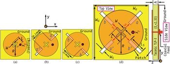
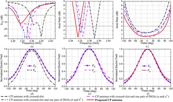
Initially, a conventional approach involving a crossed-shaped slot [Reference Ray and Mandal28] at the center of the patch is conceived to design a planar circular-shaped CP antenna, as shown in Fig. 1(a). The circular patch of radius 21.5 mm with 1.85% cross-shaped slotted area exhibits impedance bandwidth (IBW) of 2.7% (2.354–2.418 GHz), CPBW of 0.63% (2.374–2.389 GHz), and 3 dB ARBW of 128° across the angular range −68° to +60° at 2.385 GHz, as shown in Fig. 2. The antenna size is reduced by 0.17λ 0 (0.5–0.33λ 0) due to the crossed-shaped slot at the center of the patch [Reference Zheng and Chu29].
Evolution of the proposed CP antenna: (a) CP antenna with crossed-slot, (b) CP antenna with crossed-slot and one pair of DGSs (a and a′), (c) CP antenna with crossed-slot and one pair of DGSs (b and b ′), and (d) proposed CP antenna with crossed-slot and two pairs of DGSs [parameters dimension: W G = 65.2 mm (0.5λ 0), h = 1.575 mm (0.012λ 0), 2R = 43 mm (0.33λ 0), L = 13.4 mm (0.1λ 0), W = 1 mm (0.0076λ 0), L S = 14 mm (0.11λ 0), W S = 1 mm (0.0076λ 0), S = 24 mm (0.18λ 0)] [λ 0 = free space wavelength corresponding to the CP frequency 2.306 GHz].

Analysis of different antenna structures: (a) S 11 versus frequency, (b) AR versus frequency, and (c) 3 dB ARBW versus theta (θ); the $E_\theta$ and $E_\varphi$
 components for (d) CP antenna with crossed-slot (e) CP antenna with crossed-slot and one pair of DGSs, and (f) proposed CP antenna [φ = 0° plane].

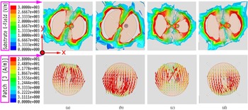
Now, to overcome the beamwidth hurdle, two narrow slots (a and a′) of only 0.4% fractional area of the ground plane are etched along the diagonal line of the ground plane. Here, the narrow slots are the small defects on the ground plane and presented as a pair of DGSs with an optimum gap of 20.2 mm, as shown in Fig. 1(b). This antenna offers IBW of 2.8% (2.3–2.367 GHz), CPBW of 0.6% (2.325–2.339 GHz), and 3 dB ARBW of 154° across the angular range −76° to +78° at 2.332 GHz, as shown in Fig. 2 and the achieved 3 dB ARBW is only 26° incremental concerning the initial design (Fig. 1(a)). To review the roots of poor 3 dB ARBW, the electric field distribution in the substrate and the patch surface currents are investigated, as shown in Fig. 3(a). The asymmetric electric field in the substrate (Fig. 3(a)) restricts the higher magnitude current components across the limited area on the patch lead to a narrower 3 dB ARBW in the antenna.
Electric field distributions in substrate (upper) and surface current on the patch (lower) for different structures: (a) crossed-slot with one pair of DGSs (a and a′) at 2.332 GHz; crossed-slot with two pairs of DGSs with (b) S = 0.18λ 0 at 2.312 GHz (proposed), (c) S = 0.01λ 0 at 2.222 GHz, and (d) S = 0.27λ 0 at 2.371 GHz [all distributions are taken under the same scale].

Similar behavior is perceived in a CP antenna (Fig. 1(c)) with one pair of DGSs (b and b′) along the other diagonal line, which exhibits IBW of 2.5% (2.299–2.356 GHz), CPBW of 0.5% (2.317–2.328 GHz), and 3 dB ARBW of 156° across the angular range −80° to +76° at 2.323 GHz, as shown in Fig. 2. To enrich the 3 dB ARBW further, the orthogonal arrangement of DGS pairs (a − a′ and b − b′), along the two diagonals of the ground plane, is conceived, as shown in Fig. 1(d). This structure is considered as the proposed planar CP antenna offering IBW of 2.4% (2.29–2.344 GHz), CPBW of 0.65% (2.303−2.318 GHz), and the 3 dB ARBW of 180° across the angular range −88° to +92° at 2.312 GHz, as shown in Fig. 2. The dimension of each DGS is finalized as (L S × W S). The distance parameter (S) between the paired-DGSs is finalized at 0.18λ 0 after analyzing Fig. 3(b–d). The collective performance of the enhanced current distribution across the patch surface and a reduction of orthogonal components solve the lower 3 dB ARBW issue of the two primary antennas (Figs 1(b) and 1(c)). For S = 0.01λ 0 (Fig. 3(c)), the asymmetric substrate field distribution concentrates only along the x-axis, and subsequent higher magnitude current components are also concentrated across a limited area along x-axis of the patch with a significant amount of orthogonal current components (x-directed). For S = 0.27λ 0, the substrate field distribution is not symmetric about the centerline of the patch, and the higher magnitude current components are decreasing across the patch, as shown in Fig. 3(d). However, for S = 0.18λ 0 (the proposed position of DGS pairs, Fig. 3(b)), it displays symmetric substrate field distributions with reduced x-directed current components, which collectively uplift the 3 dB ARBW by 40.62% in comparison to the basic CP antenna (Fig. 1(a)), as illustrated in Fig. 2. When S = 0 (crossed-shaped DGS), the antenna losses its CP property and show an AR above 3 dB.
The two far-field components $E_\theta$ and $E_\varphi$
 define the axial ratio of CP characteristics in the antenna radiation. It can be observed that the 3 dB ARBW is progressively improved from CP antenna with crossed slot to one pair of DGSs and two pairs of DGSs. Therefore, it is important to notice the beamwidth variation of $E_\theta$
 and $E_\varphi$
 across elevation angle (θ) for different structures of the CP antenna shown in Fig. 2(d)–(f). For the proposed structure, better matching between $E_\theta$
 and $E_\varphi$
 is observed across a wide angular range, leading to higher ARBW.
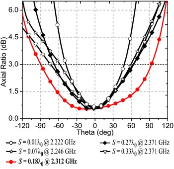
From discussions on Fig. 3, it is traced that the electric field in the substrate and the surface current on the patch can be controlled effectively with the appropriate placement of the paired-DGSs. Further, the principle of wider 3 dB ARBW can be explicated in the following analysis. When the slot width W S ≪ λ 0, the electric field varies as a cosine function along the slot length (L S) [Reference Gupta, Garg, Bahl and Bhartia30]. Based on this theory, the magnitude of the two far-field components ($E_\theta$ and $E_\varphi$
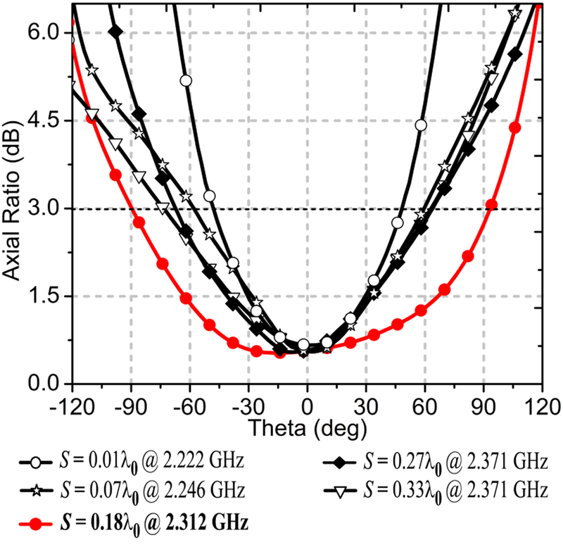
 ) in the XZ-plane varies with the gap (S) between the DGSs pairs as a function of elevation angle theta (θ), along with their corresponding AR at the principal plane φ = 0°, as shown in Figs 4 and 5, respectively. It is observed that the magnitude of $E_\theta$
 is almost unchanged irrespective of S, as $E_\theta$
 is not a function of S variations. Therefore, only for the proposed S value (S = 0.18λ 0 at 2.312 GHz), the $E_\theta$
 plot (plot in red color) is included. However, the magnitude of E φ gradually falls as S is incremented from 0.01λ 0 to 0.07λ 0 and 0.18λ 0. Specifically, for S = 0.01λ 0, wider flatness in $E_\varphi$
 plot across θ = 0° is observed, which is far away from $E_\theta$
 . When S = 0.18λ 0, the magnitude of $E_\varphi$
 dramatically drops and it becomes nearly equal to $E_\theta$
 across a wide range of θ. As a consequence, the 3 dB ARBW of the proposed CP antenna is extended to 180° at φ = 0° plane. For other values of S (S > 0.18λ 0), magnitude of $E_\varphi$
 again continues to increase and appear far away from $E_\theta$
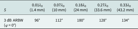
 . Hence, a continuance of lower 3 dB ARBW is detected. Therefore, the above investigation shows that the position of the pairs of the DGSs plays a crucial role in uplifting the 3 dB ARBW of the proposed CP antenna. A summary of all quantitatively exemplified 3 dB ARBW for different values of S is tabulated in Table 1. From the realization of maximum 3 dB ARBW, S = 24 mm (0.18λ 0) is selected for the final design.
Simulated $E_\theta$ and $E_\varphi$
 for different choices of S in the XZ-plane.

Simulated AR for different choices of S at the plane of φ = 0°.
3 dB ARBW for different selections of S

From the surface current distributions on the patch (Fig. 3), it is found that the higher magnitude current component symmetrically increases across the patch surface as S is increased from 0.01λ 0, to 0.18λ 0. This phenomenon of higher magnitude current components further relates to the beamwidth principle of the $E_\varphi$ component. The magnitude of $E_\varphi$
 across theta (θ) is decreasing with the increase of S from 0.01λ 0 to 0.18λ 0, and it approaches to the $E_\theta$
 component, as demonstrated in Fig. 4. It also confirms the insensitive property of $E_\theta$
 to S. The higher magnitude current component does not influence the magnitude of $E_\theta$
 . For a further increment of S (>0.18λ 0), the magnitude of $E_\varphi$
 across theta (θ) is increasing (Fig. 4), as symmetries of higher magnitude current components across the patch surface are reduced (Fig. 3(d)). Hence, the beamwidth of $E_\varphi$
 across theta (θ) is noticed to appear far away from $E_\theta$
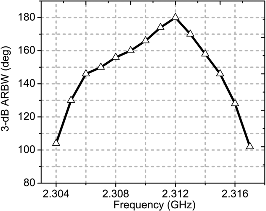
 . Therefore, a linear relationship has been observed between the symmetries in higher magnitude current components across the patch surface and the magnitude of E φ far-field component. It is observed in Fig. 6 that across 86.6% of the entire CP band, the 3 dB ARBW is more than 100°, which strongly validates the practicality of the proposed CP antenna.
Peak values of 3 dB ARBW (simulated) across the entire CPBW in φ = 0° plane.

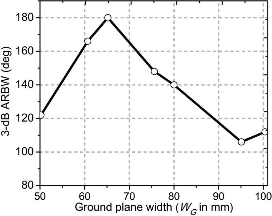
Intrinsically, the metallic ground plane takes the role of a backed reflector for the antenna. Therefore, the influence of the ground plane on the 3 dB ARBW of the proposed CP antenna needs to be analyzed, and these are summarized in Fig. 7. It is found that the 3 dB ARBW reaches to its maximum value of 180° for the proposed size (W G = 65.2 mm) of the ground plane.
The 3 dB ARBW for several width (W G) of ground plane.

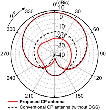
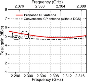
Finally, to observe the impact of DGSs pairs on the back radiation performance, the radiation pattern of the proposed CP antenna (Fig. 1(d)) has been compared with a conventional CP antenna without DGS (Fig. 1(a)), as shown in Fig. 8. It is observed that narrow slotted DGSs pairs do not affect the back radiation and the front-to-back ratio of the proposed CP antenna. Additionally, the cross-polarization discrimination (XPD) of the proposed CP antenna is significantly increased with this proposed DGS technique by 5 dB in comparison to the conventional CP antenna. Further analysis of the DGSs performance on the proposed CP antenna exhibits a 0.17 dBic gain enhancement compared to a conventional CP antenna without DGS, as shown in Fig. 9.
The simulated radiation pattern of the conventional CP antenna without DGS and proposed CP antenna (φ = 0° plane).

The simulated peak gain of the conventional CP antenna without DGS and proposed CP antenna across their entire CPBW.

Experimental results
Based on the optimized dimensions obtained from above design principle, the final proposed design (Fig. 1(d)) was fabricated on a 65.2 mm × 65.2 mm Taconic TLP-3 substrate, with dielectric constant ($\epsilon _r$ ) = 2.33, loss tangent (tanδ) = 0.0009, and thickness (h) = 1.575 mm.
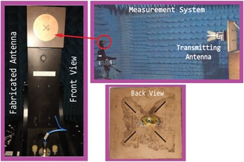
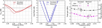
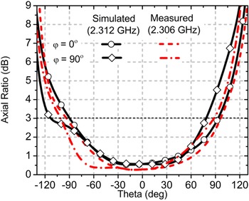
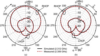
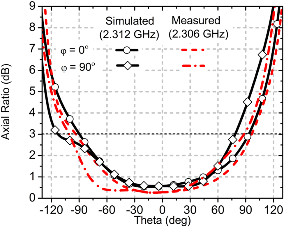
The photographs of the fabricated prototype and its experimental setup are shown in Fig. 10. Reasonably good matching between the simulation and measurement results is observed. The measurements indicate IBW (S 11 ≤ −10 dB) of 2.6% (2.283–2.342 GHz), CPBW of 0.9% (2.294–2.315 GHz), the realized peak gain higher than 4.8 dBic, and the total antenna efficiency more than 64% across the entire CP band, as summarized in Fig. 11. The measured 3 dB ARBW of the proposed CP antenna extends up to 186° and 188° at φ = 0°, and φ = 90° planes, respectively, as shown in Fig. 12. It is observed that the antenna features a good CP purity (AR < 1 dB) across a wide-angle of theta (θ) −48° to +46° at φ = 0° plane. The measured and simulated radiation patterns are in the broadside direction for φ = 0° and φ = 90° planes, as shown in Fig. 13. From these radiation patterns, the estimated half power beamwidth is 88° and 82° at the plane of φ = 0° and φ = 90°, respectively, which are widely recommended for low-profile planar CP antennas in practice. The radiation patterns in both of the principal planes, as shown in Fig. 13, are confirming the right-handed circular polarization (RHCP) behavior of the proposed CP antenna. An adequate amount of cross-polarization discrimination (XPD = 28 dB) between RHCP and left-handed circular polarization (LHCP) is observed in both the principal planes. This level of performance is acceptable for the CP antenna's practical implementation.
Photos of the fabricated prototype and experimental setup.

Plots of simulated and measured (a) reflection coefficients (S 11), (b) AR, and (c) gain and the total efficiency of proposed CP antenna.

The 3 dB ARBW of proposed CP antenna at φ = 0° and φ = 90° planes.
The simulated and measured RHCP and LHCP patterns at (a) φ = 0°, and (b) φ = 90° planes.

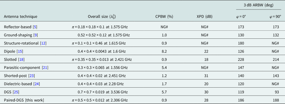
The measured results of the proposed CP antenna are benchmarked against other wide beamwidth CP antenna designs reported in literature, as summarized in Table 2. The comparison encompasses some significant parameters such as overall dimension, 3 dB ARBW, and XPD. In both the principal planes, the proposed CP antenna shows the highest 3 dB ARBW except the work in [Reference Ray, Mandal, Nasimuddin, Lalbakhsh, Raad and Tubbal18], along with acceptable CPBW (0.9%) and better XPD (28 dB) values. It is found that the proposed DGS integration technique provides 10 dB better XPD than the previous work [Reference Ray, Mandal, Nasimuddin, Lalbakhsh, Raad and Tubbal18]. Hence, the strategically placed narrow DGSs can convert a conventional CP antenna to a wide-beamwidth CP antenna along with better XPD. The realized CPBW is comparable with major related works and has sufficient quality for wide beamwidth narrowband applications. Overall, the proposed antenna exhibits superior CP performance while retaining a compact and geometrically simple structure.
Compared measured results of proposed CP antenna with other related works

#NG: The data were not provided in the respective reference.
Conclusion
The incorporation of customized DGSs for beamwidth enhancement of slot-loaded planar CP antenna is demonstrated successfully. The presented methodology leads to a low-profile CP structure featuring a wide 3 dB ARBW, which offers considerable performance improvements over similar designs reported in the literature so far. In the proposed design, the surface current distribution and its orthogonal components on the patch can be controlled easily with the proper placement of paired-DGSs. The enhancement of higher magnitude current and reduction of orthogonal current components across the patch surface promises a 3 dB ARBW across a wide angular range. Relationships between physical parameters, electric fields, surface currents, and the 3 dB ARBW are established based on the comprehensive design analysis. The proposed CP antenna, with its competitive features, can be employed in navigational systems and also for space communications.
Acknowledgements
The authors would like to acknowledge Prof. Kumar Vaibhav Srivastava of IIT Kanpur, India for providing their measurement facilities. This work is financially supported by University Grants Commission (UGC), Govt. of India under National Fellowship for SC (NFSC) Ph.D. scheme (Award Letter No.: F1-17.1/2017-18/RGNF-2017-18-SC-WES-32056/(SA-III/Website)).
Conflict of interest
None.
 Mrityunjoy Kumar Ray received his B.Tech. degree in electronics and communication engineering from Maulana Abul Kalam Azad University of Technology (MAKAUT), West Bengal, India in 2006 and M.Tech. degree in electronics design and technology from Tezpur University, Assam, India in 2009. He is currently pursuing Ph.D. (Tech.) degree at the Institute of Radio Physics and Electronics, University of Calcutta, West Bengal, India. He had worked as an assistant professor at Greater Kolkata College of Engineering and Management. His current research interests include wide beamwidth and wide bandwidth circularly polarized microstrip antenna.
 Kaushik Mandal received his B.Sc. degree in physics (H), B.Tech., and M.Tech. degrees in radio physics and electronics from the University of Calcutta, in 2001, 2004, and 2006, respectively. He received his Ph.D. (Tech.) from the University of Kalyani, in July 2014. Since 2016 he is working as an assistant professor in the Institute of Radio Physics and Electronics, University of Calcutta, West Bengal, India. He has authored or co-authored 51 internationally refereed journal papers along with an international patent. His current research interests include the design of circularly polarized antennas, SIW integrated microstrip antennas, MIMO antennas for sub-6 GHz applications, and performance enhancement of microstrip antennas using frequency-selective surface (FSS) and metamaterial. Dr. Mandal is a senior member of IEEE. He served as the secretary of IEEE AP-MTT Chapter, Kolkata Section for the years 2020, 2021, and 2023.
 Gholamhosein Moloudian received the associate's degree in Electronics from Technical and Vocational University of Yasouj (First-Class Hons), the B.Sc. degree in electronics engineering from Higher Education Center of Shiraz, the M.Sc. degree in electronics engineering from Islamic Azad University (IAU) Bushehr (First-Class Hons), and the Ph.D. degree (excellent grade) in electronics engineering from IAU, Arak Branch, Iran, all in electrical engineering with the highest honors, in 2008, 2010, 2012, and 2018, respectively. He is currently working with the Wireless Sensor Network group (antenna/RF team), Tyndall National Institute, University College Cork (UCC), Ireland, as a Marie Skłodowska-Curie Researcher, SMART 4.0 Fellow (Smart manufacturing SFI/CONFIRM Center). His research interests include design and analysis of RF/microwave circuits, RF energy harvesting circuits, RFID, rectifying antenna (rectenna), smart sensors, microstrip antennas, photonic devices, smart industry 4.0, and biomedical sensors and antennas.
 Ali Lalbakhsh received the B.S. and M.S. degrees in electronic and telecommunication engineering from Islamic Azad University, Iran, in 2008 and 2011, respectively. He received the Master of Research degree (HD) and the Ph.D. in electronics engineering from Macquarie University, Australia in 2015 and 2020, respectively, and he is currently a sessional academic in the same institution. He has 70 research publications. His research interests include artificial intelligence, electromagnetic structures, microwave components, and evolutionary optimization methods. Dr. Lalbakhsh received several prestigious awards. Ali is the only researcher in IEEE Region 10 (Asia-Pacific) who has won the most prestigious Best Paper Contest of IEEE Region 10 more than once. He was awarded first, second, and third prizes in this international competition in 2018, 2019, and 2016, respectively. Ali is as an associate editor of AEÜ – International Journal of Electronics and Communications.