I. INTRODUCTION
The development of concepts such as the Internet of Things (IoT), Smart Cities, and Machine-to-Machine communications is increasing the demand for autonomous, self-powered devices that are capable of collecting energy from the surrounding environment in order to power up and operate. This increasing demand of self-sustained devices, which can operate without requiring any battery to power up, has led to the development of a wide variety of energy-harvesting and wireless power transmission solutions toward providing this autonomy [Reference Georgiadis, Andia-Vera and Collado1–Reference Vyas, Nishimoto, Tentzeris, Kawahara and Asami5]. Energy harvesters for solar, electromagnetic (EM), thermal, and vibration energy have been developed using different technologies and concepts. Owing to the uncertainty and variability in the levels of available energy from these types of energy sources, the development of hybrid energy harvesters has been considered [Reference Georgiadis, Collado, Via and Meneses6, Reference Collado and Georgiadis7] as a way to ensure that there is always enough energy to operate the selected devices. Toward the same objective the use of wireless power transmission has also been considered, where an intentional radio frequency (RF) signal with a certain frequency and power level is transmitted to power up devices up to large distances [Reference Shinohara8].
When utilizing hybrid harvesters, it is important to perform an efficient combination of the two DC outputs obtained from each of the harvesting solutions. In this paper, a novel DC combining circuit that can be used in solar/EM energy harvesters or solar/wireless power transmission systems is presented. The circuit is aimed to combine the DC outputs both from the rectifier circuit and from the solar cells minimizing the losses and mismatches that can appear when combining different DC levels [Reference Shinohara and Matsumoto9, Reference Popovic10].
The proposed DC combining circuit is used in a solar rectenna structure that is capable to harvest solar ambient energy and EM radiation at 2.45 GHz, providing a certain amount of power to a selected sensor platform. The EM harvester has been designed following a low-profile, cavity-backed slot antenna topology, based on a substrate-integrated waveguide (SIW) technology, as already proposed in [Reference Giuppi, Georgiadis, Collado and Bozzi11, Reference Giuppi, Georgiadis, Bozzi, Collado and Perregrini12]. Cavity-backed antennas can be useful in many applications, as the metallic walls of the cavity help reducing the radiation leakage through the substrate, and the additional metal surface permits to deal with the heat that can eventually be produced under certain operation conditions or environments. Amorphous silicon (a-Si) solar cells are integrated on top of the antenna structure allowing for a compact implementation of the solar/EM harvester [Reference Georgiadis, Collado, Via and Meneses6, Reference Collado and Georgiadis7, Reference Danesh and Long13, Reference Tanaka, Suzuki, Suzuki and Araki14].
The designed solar/EM harvester is intended to interface with a commercial wireless sensor node (WSN) setup. The circuit performance has been optimized in order to satisfy the specifications required by the sensor.
Section II is dedicated to the definition of the WSN environment in which the designed EM/solar harvester is intended to be employed with particular attention to the voltage and power levels needed for the sensor node to operate. Section III focuses on the design of the SIW cavity-backed slot antenna to be used in the rectenna design. This section also describes the integration of the solar cells together with the antenna structure and the sensor nodes enclosure. In Section IV, the design of a DC combining circuit, which permits combining the power coming from the EM and solar sources and presents a unique DC voltage and power level at the input of the sensor node circuitry, is presented. Section V concludes the paper by highlighting the achieved results.
II. APPLICATION SCENARIO AND REQUIREMENTS
The design of the hybrid energy harvester has to be done considering the targeted final application, as the requirements may vary considerably depending on several factors. Here the proposed hybrid energy harvester is intended to be used in a self-powered sensor node platform for building monitoring.
The choice of the energy sources for the harvester is strongly influenced by the environment in which the sensor platform is intended to operate. If the operation scenario is outdoor or indoor, one can consider the presence of solar or artificial light that can be easily harvested by properly dimensioned solar panels. In addition to that, other energy sources can be considered such as vibration, thermal or EM. Here, EM energy harvesting has also been considered to power up the sensor platform as it can also be present both in indoor and outdoor scenarios. In the next sections, the WSN application targeted and the associated specifications in terms of required power are discussed.
A) Application scenario
The need for self-powered sensor nodes in a WSN application is of great importance under particular operating conditions. Nowadays, wireless sensor networks are used in many aspects of everyday life. Among the most common applications stand the security in buildings, as well as their structural stability monitoring, and the control of certain environments (seismic areas, factories, and dangerous places). As a result, there is a need for a large number of sensors, which are sometimes placed in locations that are difficult to reach, which makes it challenging and expensive to take care of their maintenance.
The application scenario that has been targeted here is a WSN for building monitoring. The WSN monitors a wide variety of parameters, such as stability, temperature and humidity in a mixed indoor/outdoor environment.
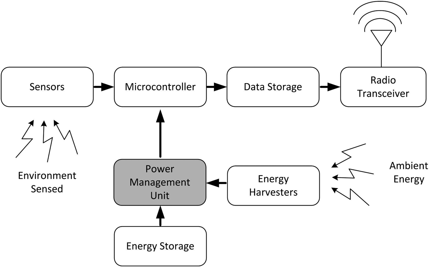
In order to get advantage of the natural and artificial light that can be harvested in the external part of a building and in the rooms inside, it has been decided to use the solar energy as the main power source for the sensor. In addition to that, EM energy harvesting has been considered, as RF signals are also present both inside and outside the building and light might not always be present. The proposed harvester is a hybrid solar/EM harvester. The collected energy from both solar and EM sources is processed as illustrated in Fig. 1 and stored, in order to be used for powering the WSNs.
Block diagram of the sensor network platform.

B) Selected requirements
The architecture used in the WSN scenario selected is shown in Fig. 1. The sensor platform operates taking energy from ambient energy sources by means of the proposed hybrid solar/EM harvester. A power management circuit boosts the harvested DC voltage, and store the energy in a battery or supercapacitor. It also handles the stored energy and delivers it to the microcontroller whenever it needs power to operate.
On the other side, the sensor platform collects information about the surrounding environment by means of different sensor devices that convert the received physical measurement to an electrical signal that is handled by the microcontroller and then stored. The stored information is send to a base station by means of a radio transceiver and a communication antenna.
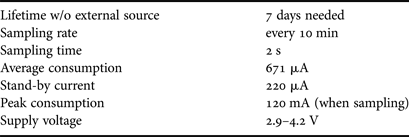
The requirements of the sensor platform of Fig. 1 are listed in Table 1.
Sensor operation requirements.
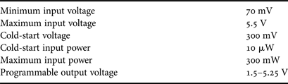
The Texas Instrument BQ25504 evaluation kit was chosen to integrate the power management unit as it is capable of handling ultra-low power input power levels. It contains a boost converter that incorporates a DC-to-DC conversion stage plus a regulator. Its main specifications are shown in Table 2. One can see that it can boost input voltages as low as 70 mV. The boost converter is configured to allow a connection between the power management unit and the sensor if the storage voltage falls in the desired range between 2.9 and 4.2 V. This prevents the energy storage element to charge too much, or to discharge below a desired level.
BQ25504 specifications.
The selected storage element for the targeted application is a supercapacitor. The dimensioning of the supercapacitor element is done assuming that the sensor platform needs to be able to operate for 7 days without any external energy contribution and consuming an average of 671 µA. Considering this requirements, it was calculated that a 350 Farad capacitance is enough to guarantee this performance. The selected supercapacitor is the BCAP0350 from Maxwell.
III. SOLAR ANTENNA DESIGN
In a current WSN environment, the design of the blocks that are directly connected with the external world, like the energy harvesting module, is getting more and more challenging; in fact, the device should be robust and compact, in order to be placed anywhere. In addition to that, particular attention is devoted to the implementation costs that need to be low if the device is intended for extensive mass production.
A) SIW cavity-backed slot antenna
Substrate Integrated Waveguide technology is adopted for the implementation of a cavity-backed slot antenna. In the designed structure an SIW cavity encloses the radiating element (a slot), in order to create a cavity-backed configuration (Fig. 2).
SIW cavity-backed slot antenna (a) antenna layout, (b) fabricated prototype, (c) solar antenna prototype.
The design is made in FR4 of 1.6 mm height, dielectric constant ε r = 4.4 and loss tangent tanδ = 0.02. The input 50 Ω line is placed on one side of the substrate board, whereas on the other side a slot is used as radiating element. The structure is dimensioned to operate at 2.45 GHz.
B) Integration with solar cells and sensor packaging
The structure of the solar antenna is based on the SIW cavity-backed slot antenna presented in the previous section. An a-Si solar cell is integrated on top of the antenna structure (Fig. 2). The location of the solar cell is selected in order to avoid affecting the performance of the antenna itself. This is done by placing the solar cells in an area of the antenna where the field distribution is weak. In this case avoiding covering the area surrounding the slot is enough to avoid affecting the antenna performance.
As the proposed solar/EM harvester is designed to be integrated in a polycarbonate box with a transparent cover, the final design of the solar antenna was done adding on top an additional layer of polycarbonate with ε r = 2.1 and tanδ = 0.005.
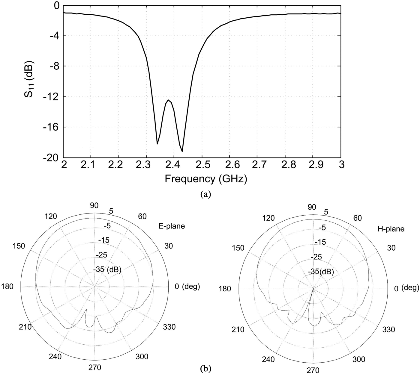
The measured input matching and radiation patterns for the final designed solar antenna together with the polycarbonate layer are shown in Figs 3(a) and 3(b) respectively. It can be seen that the antenna presents good matching around 2.45 GHz and that its gain is approximately 1.9 dB at the broadside direction.
Measured performance of the solar antenna (a) input matching, (b) radiation patterns.
IV. RECTENNA AND DC COMBINING CIRCUIT DESIGN
The proposed harvester needs a DC-combining stage that takes the DC power contributions from the solar cells and from the RF signals and combines them before delivering them to the power management circuit. This function is performed by the novel circuit proposed in Fig. 4.
Solar/EM DC-combining circuit (a) schematic, (b) photo of the implemented prototype.
Included in this DC-combining circuit, there is the rectifier element that converts the RF signals into DC power. The antenna is connected to the rectifier circuit and the obtained DC voltage is summed to the DC power coming from the solar cells by properly merging the rectifying stage with the solar harvester circuitry.
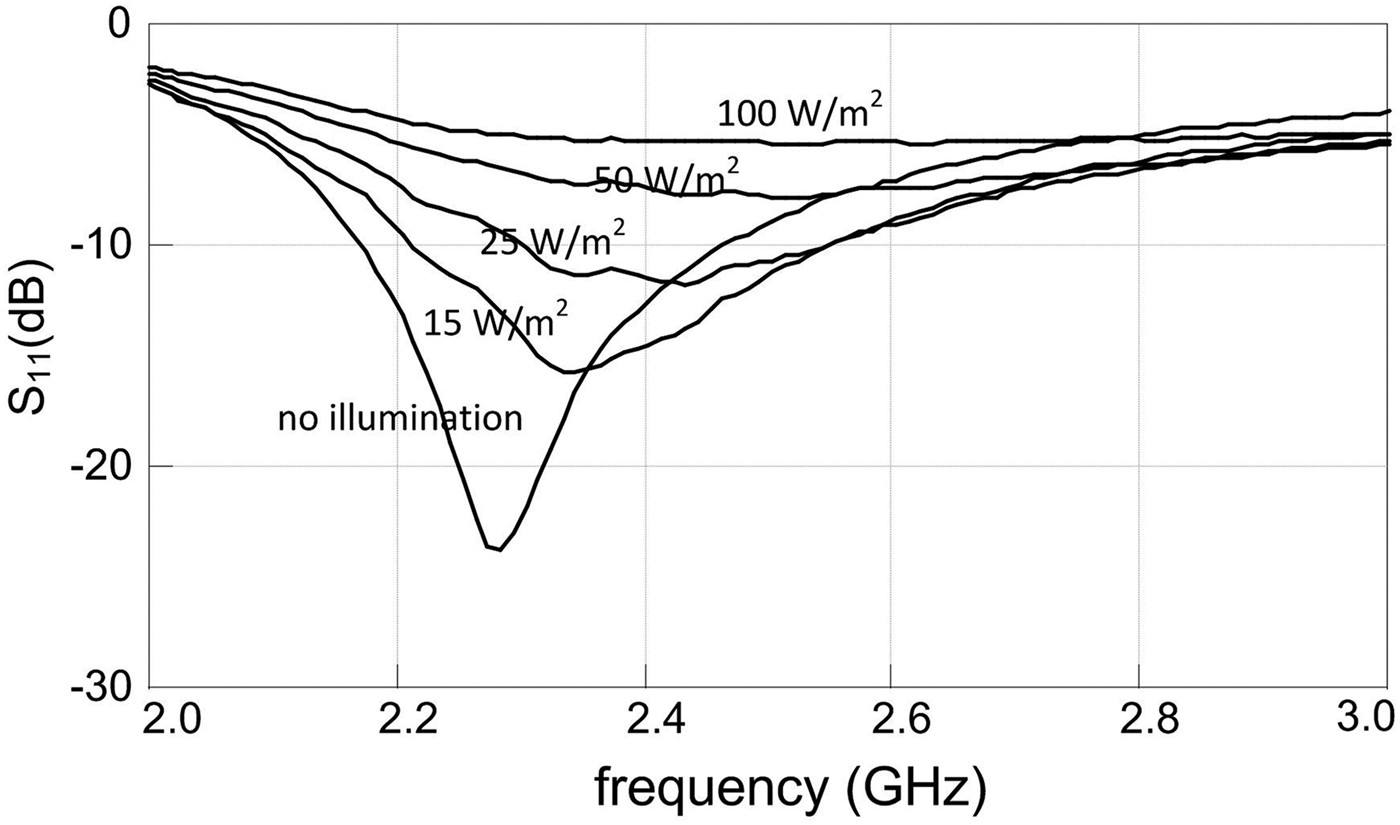
Changes in the irradiance value produce a change in the loading effect of the solar cells. In order to avoid the mismatch between the antenna and the rectifier circuit when the irradiance changes two branches are used in the DC-combining circuit. Each of the branches has a matching network and an envelope detector. The outputs of both envelope detectors are connected to an output load of 1.5 kΩ. The input matching of the DC-combining circuit for different irradiance values is shown in Fig. 5.
DC-combining circuit input matching for different irradiance values.
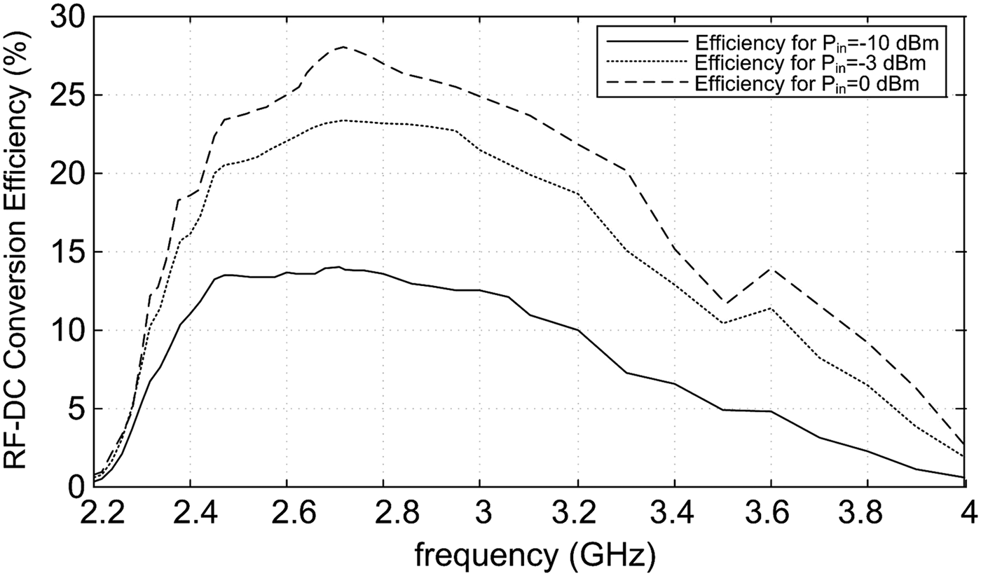
Initially, in order to evaluate the performance of the rectifier circuit, the RF–DC conversion efficiency of the DC-combining circuit is evaluated when the solar cells are completely covered and the irradiance is 0 W/m2. The RF–DC conversion efficiency is calculated using (1) and the obtained results for different RF input power levels and different frequencies are shown in Fig. 6
 $$\eta=100\ast \displaystyle{{P_{{\rm DC\_output}} } \over {P_{{\rm RF\_input}} }}.$$
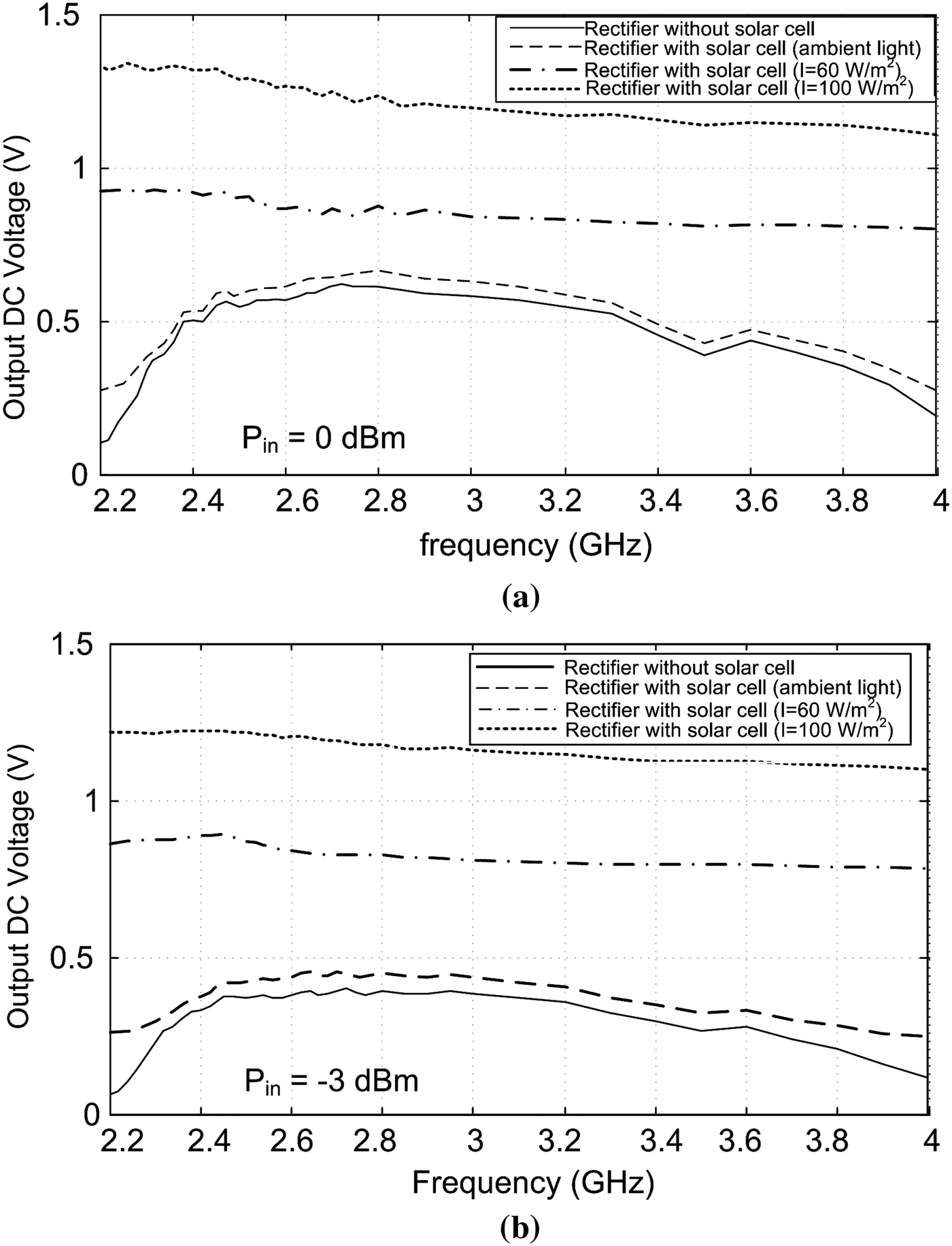
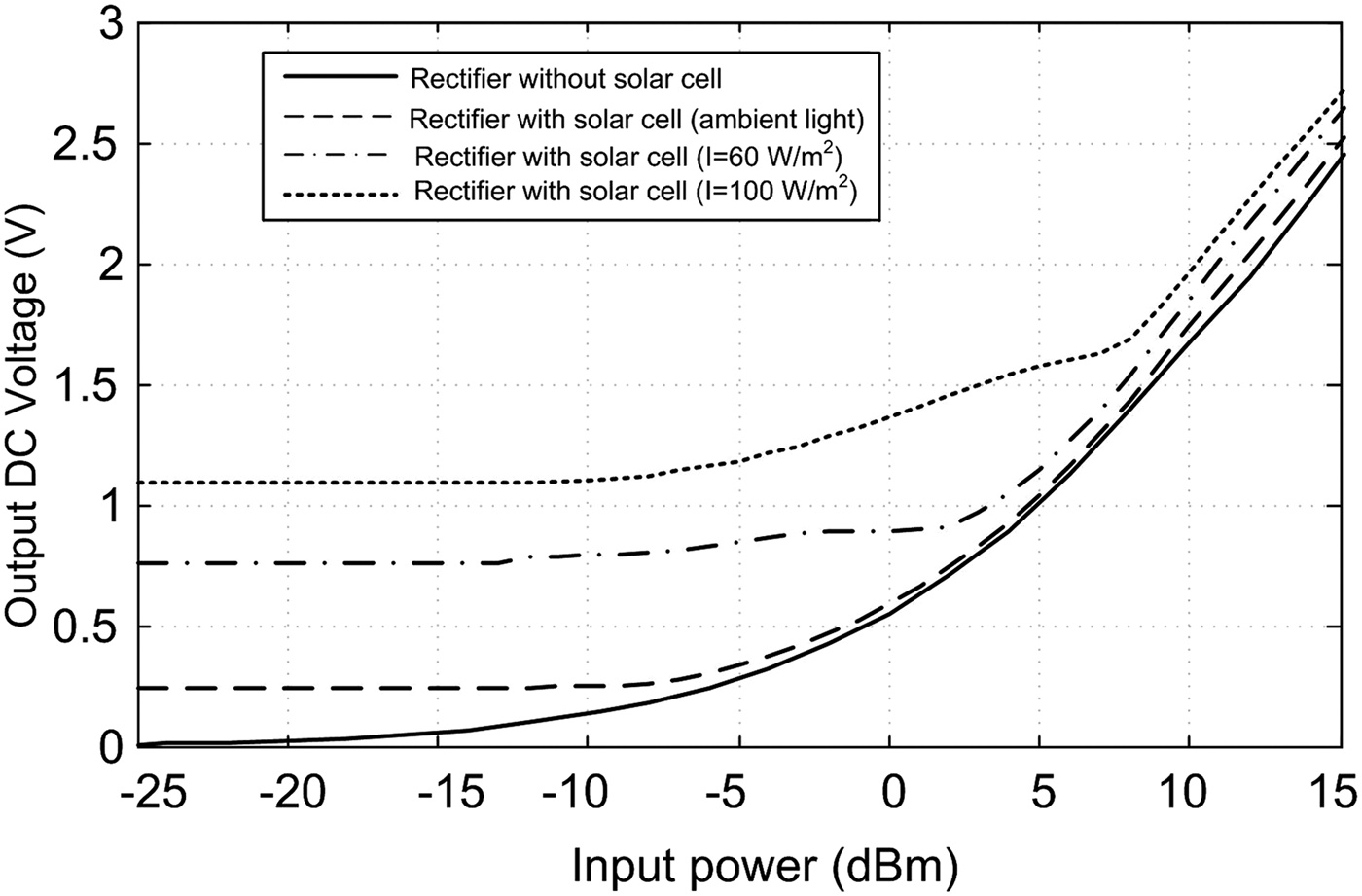
In a second step, the solar cells are uncovered and the performance of the DC-combining circuit is evaluated versus frequency for different irradiance conditions and for two different RF input power levels, 0 and −3 dBm (Fig. 7). Figure 8 shows the DC output voltage at 2.45 GHz versus RF input power level and for different irradiance values.
RF–DC conversion efficiency of the DC-combining circuit for irradiance = 0 W/m2.
DC-combining circuit output voltage versus frequency for different irradiance values (a) RF input power 0 dBm (b) RF input power −3 dBm.
DC-combining circuit output voltage versus RF input power levels for different irradiance values.
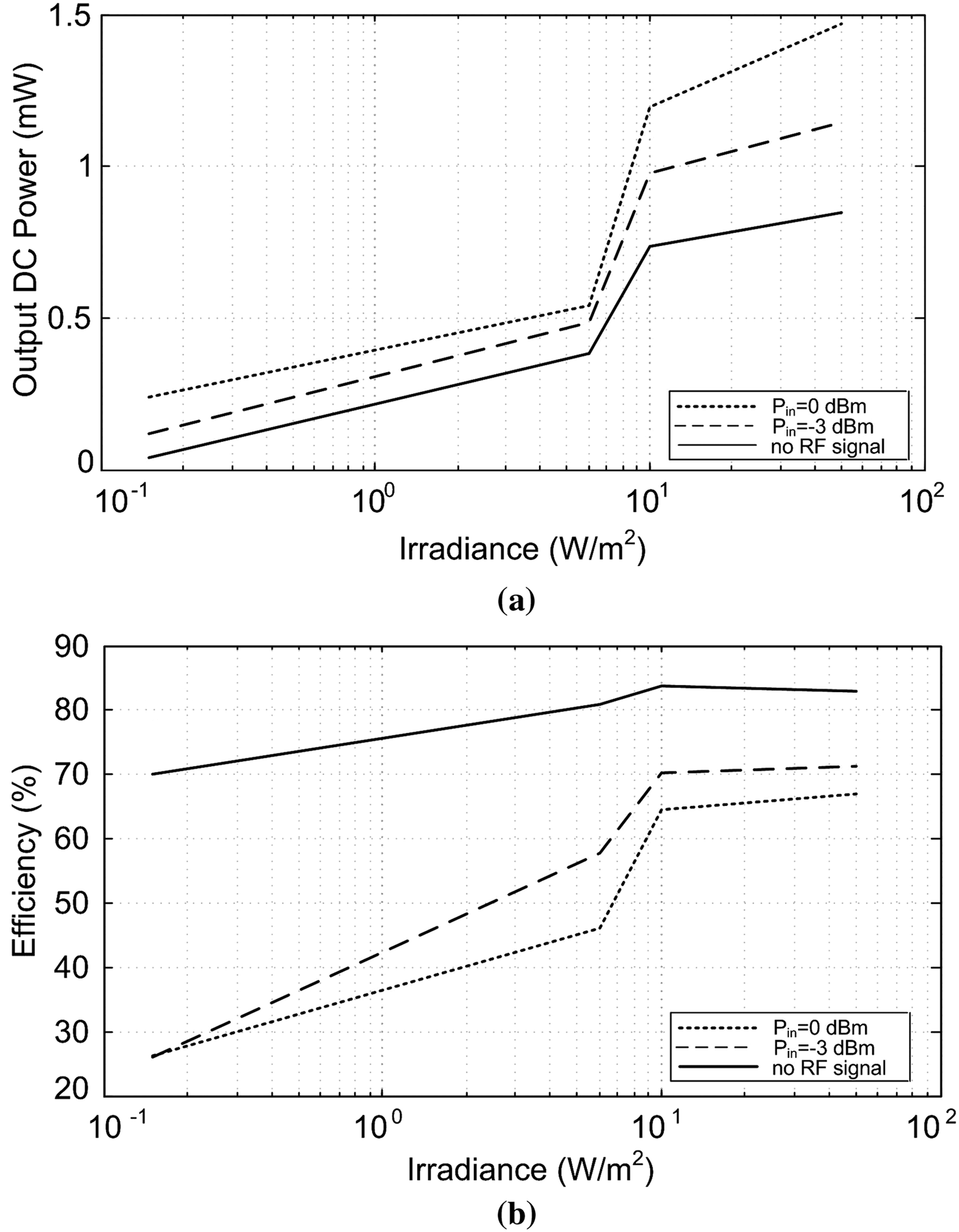
In order to evaluate the DC-combining circuit efficiency when operating simultaneously with an RF input signal and the solar cells illuminated, it is necessary to define a new figure of merit (2). The input power to the DC-combining circuit in (2) includes the RF input power and the DC power provided by the solar cell. The DC power provided by the solar cells is obtained measuring the voltage drop in the solar cell and the current flowing through it for different irradiance conditions and different RF input power levels
 $$\eta=100\ast \displaystyle{{P_{{\rm DC\_output}} } \over {\left({P_{{\rm RF\_input}}+P_{{\rm solar\_cell}} } \right)}}.$$
Figure 9 shows the combined DC output power for different irradiance and RF input power levels as well as the total efficiency of the DC combiner. It can be observed that when considering the DC output power of the solar/EM harvester, it is better to have both types of energy, solar and EM as this leads to higher values of DC power.
DC-combining circuit performance versus irradiance when simultaneously considering an RF input signal and illuminated solar cells. (a) DC output power, (b) DC-combining circuit efficiency.
However, attending to the total harvester efficiency, the best operation conditions are with high irradiance at the solar cells and no RF input signals. This concludes that the harvester should operate in the hybrid solar/EM mode when there is an immediate need of DC power to operate the sensor, and to operate only with the solar mode when there is enough light, as in this manner the generation of the DC energy to be stored is more efficient.
V. CONCLUSION
In this paper, a hybrid solar/EM harvester operating at 2.45 GHz has been presented. The proposed harvester is aimed to be used in a sensor node scenario to provide the sensors with full autonomy. A DC-combining circuit that combines the outputs from the solar and the EM harvesters is also presented, which provides a unique DC power level at its output. The proposed harvester can be very useful for its application in autonomous WSNs that cannot be easily accessed in order to avoid the periodic maintenance and battery substitution.
ACKNOWLEDGEMENTS
The authors would like to acknowledge Coilcraft, Inc. for providing the inductors used in the development of the DC-combining circuit prototype.
FINANCIAL SUPPORT
This work was supported by the Spanish Ministry of Economy and Competitiveness and FEDER funds through the project TEC2012-39143, and the EU Marie Curie FP7-PEOPLE-2009-IAPP 251557. This work was also supported by the COST Action IC1301 “Wireless Power Transmission for Sustainable Electronics (WIPE)”.
Kyriaki Niotaki was born in Crete, Greece. She received the B.S. in Informatics and M.S. in Telecommunications, from the Aristotle University of Thessaloniki in 2009 and 2011, respectively. Since December 2011, she is a research assistant with the Centre Tecnologic de Telecomunicacions de Catalunya, Castelldefels, Spain, in the area of microwave systems and nanotechnology. Her main areas of interest include energy-harvesting solutions and the design of highly efficient power amplifiers.
Francesco Giuppi was born in Pavia in 1983. He achieved the M.S. degree in Electronic Engineering at the University of Pavia in April 2008. Afterwards, he joined the Department of Electronics of the University of Pavia as a Ph.D. student in Microwave Electronics. During his Ph.D., he worked at the development of active antennas in substrate-integrated waveguide (SIW) technology. From March 2012 until August 2013, he was a post-doc at the Centre Tecnologic de Telecomunicacions de Catalunya, Castelldefels (Spain) under the Marie Curie Industry-Academia Pathways and Partnerships project Symbiotic Wireless Autonomous Powered system (SWAP).
 Apostolos Georgiadis was born in Thessaloniki, Greece. He received the B.S. degree in Physics and M.S. degree in Telecommunications from the Aristotle University of Thessaloniki, Greece, in 1993 and 1996, respectively. He received the Ph.D. degree in electrical engineering from the University of Massachusetts at Amherst, in 2002. He is currently a Senior Researcher at Centre Technologic de Telecomunicacions de Catalunya where he is leading the group of Microwave Systems and Nanotechnology and he is involved in active antennas and antenna arrays and more recently with RFID technology and energy harvesting. Dr. Georgiadis the Chair of the IEEE MTT-S TC-24 RFID Technologies and Member of IEEE MTT-S TC-26 Wireless Energy Transfer and Conversion. He serves at the Editorial board of the Radioengineering Journal and as an Associate Editor of the IEEE Microwave and Wireless Components Letters and IET Microwaves Antennas and Propagation Journals. He is Editor-in-Chief of the Wireless Power Transfer Journal by Cambridge University Press.
Ana Collado received the M.Sc. and Ph.D. degrees in Telecommunications Engineering from the University of Cantabria, Spain, in 2002 and 2007, respectively. She is currently a Senior Research Associate and the Project Management Coordinator at the Centre Tecnologic de Telecomunicacions de Catalunya (CTTC), Barcelona, Spain where she performs her professional activities. Her professional interests include active antennas, substrate integrated waveguide structures, nonlinear circuit design, and energy harvesting and wireless power transmission (WPT) solutions for self-sustainable and energy efficient systems. She has participated in several national and international research projects and has co-authored over 70 papers in journals and conferences. She is a Marie Curie Fellow of the FP7 project Symbiotic Wireless Autonomous Powered system (SWAP). She serves in the Editorial Board of the Radioengineering Journal and she is currently an Associate Editor of the IEEE Microwave Magazine and a member of the IEEE MTT-26 Technical Committee.