I. INTRODUCTION
Lead sulfide (PbS) has been widely studied in the past few decades due to its small direct band gap (0.41 eV) and large exciton Bohr radius (18 nm), which imply large quantum confinement at a fairly large scale,Reference Machol, Wise, Patel and Tanner1, Reference Kang and Wise2 and potential applications in constructing photovoltaic cells,Reference Luther, Gao, Lloyd, Semonin, Beard and Nozik3, Reference Wadia, Aalivisatos and Kammen4 lead sulfide photoconductive detectors,Reference Ghamsari, Araghi and Farahani5–Reference Theocharous8 near-infrared (NIR) light-emitting diodes, and lead chalcogenide lasers.Reference Werle, Slemr, Maurer, Kormann, Mücke and Jänker9, Reference Rogach, Eychmüller, Hickey and Kershaw10 The third-order nonlinear optical properties of PbS nanocrystals have potential applications in optimized nanoscale nonlinear optical devices,Reference Neo, Venkatram, Li, Chin and Wei11 optical switches, and thermoelectric devices.Reference Johnsen, He, Androulakis, Dravid, Todorov, Chung and Kanatzidis12 There are reports in the literature of cases when the size scales of the material hit the limit of strong quantum confinement (i.e., comparable to or less than the Bohr radius), luminescence spectra of PbS semiconductor nanostructures cover both visible and NIR regions.Reference Hines and Scholes13–Reference Acharya, Gautam, Sasaki, Bando, Golan and Ariga19 PbS nanostructures also offer great opportunities to study electron transfer behavior and electron dynamics,Reference Hyun, Bartnik, Sun, Hanrath and Wise20, Reference Patel, Wu, Zhang, Torres-Martinez, Mehra, Yang and Risbud21 (strong) confinement of charge carriers and phonon,Reference Wise22 exciton–phonon coupling, and resonant nonradiative energy transfer.Reference Machol, Wise, Patel and Tanner1, Reference Clark, Harbold and Wise23, Reference Pei and Liu24 Up to date, several methods, such as sonochemical, microwave irradiation, thermal decomposition, radiolytic method, as well as hot-injection synthesis, have been utilized to prepare cubic, granular, truncated cubic, rod-shaped, and zero-dimensional nanostructured materials.Reference Wang, Gu and Lu25–Reference Jiao, Gao, Lu, Chen, Zhou and Li29
The properties of nanocrystals depend not only on their chemical composition but also on their structure, phase, shape, surface modification, size, and size distribution. A lot of effort has been made to prepare heterostructure materials and to determine their properties because the retention of initial surface state is a key for obtaining high performance and stable materials. Meanwhile, semiconductor heterostructures combining two or more materials provide further opportunities for tailoring electronic functionalities. And they include a large variety of semiconductors, although research in this area is dominated by core/shell II–VI semiconductor heterostructures featuring a direct band gap. The architecture control of nanomaterials with well-defined shapes is important for the success of “bottom-up” approaches toward further nanodevice fabrications. To low the release of highly toxic heavy metal ions and to enhance the material performance, PbS/ZnS core–shell nanostructures were prepared.Reference Acharya, Gautam, Sasaki, Bando, Golan and Ariga19 Furthermore, silica layers were coated via a modified Stöber method to get water-soluble and biocompatible nanostructures.Reference Wang, Gu and Lu25 However, the effect of coated degree has never been studied, and the properties on electric field have never been determined.
In this article, the truncated cubic PbS nanocrystals were first prepared by a reflux method using hexadecyltrimethylammonium bromide (CTAB) as a template and stability agent, which is simpler and more environmentally friendly than other methods. Then, monodisperse ZnS/CdS partly coated and ZnS-/CdS-encapsulated PbS nanostructures are prepared via a mild conventional high yield and facile aqueous route. At last, we propose to consult an idea about impedance and permittivity measurements to provide comparative proof of the existence of heterogeneous outer layer based on the similar phenomenological model. To the best of our knowledge, this is the first time that properties under macroscopical electric field are determined.
II. EXPERIMENTAL
A. Sample preparation
All the reagents were analytical grade purity and were used without further purification. The pure water was double distilled and further deionized to have an electrical resistance higher than 18 MΩ/cm.
1. Preparation of PbS nanostructures
Truncated cubic PbS nanocrystals were prepared following the procedure described in a previous paper with slight modification.Reference Zhou, Lu, Xiu, Wang, Zhang, Zhou and Wang26 Typically, 2.7 g of CTAB and 1.14 g of lead(II) acetate trihydrate [Pb(Ac)2] were dissolved in 80 mL of pure water in a beaker and stirred at room temperature for 4 h to form a homogeneous Pb–CTAB stock solution. And thioacetamide (TAA) stock was prepared by dissolving 0.68 g of TAA in 20 mL of pure water in another beaker. The resulting Pb–CTAB stock was heated to 50 °C, and TAA stock was added dropwise to the Pb–CTAB stock, while the solution was kept vigorous stirring. As the reaction proceeded, the mixture underwent gradual change in color from milk white to gray. The mixture was then transferred to a round bottom three-necked flask equipped with a water condenser, heated to the boiling state within 5 min, and refluxed for as long as 2 h to promote the growth of PbS nanostructures. At the desired time, the resulting black solid fraction was isolated from the growth mixture by centrifugation (16,000 rpm, 5 min) and washed with ethanol and water three times. Finally, the PbS powder was kept in a vacuum dryer at 45 °C for 5 h. Pure ZnS and CdS samples used as a contrast in spectrum and electrical properties measurements were synthesized under the same condition.
2. Preparation of ZnS-/CdS-encapsulated PbS nanostructures
Here, take ZnS-encapsulated PbS nanostructures as a typical example. To prepare a stock solution of PbS nanostructures, 0.36 g of as-prepared samples were added to 45 mL of pure water in a three-necked flask, and the mixture was sonicated for 15 min; then, 0.17 g of TAA and 1.35 g of CTAB were dissolved in by vortexing. After heated to boiling temperature, the stock solution was added with a 0.1 M solution of Zn(Ac)2drop-by-drop in a quantity that the molar ratio of TAA:Zn was 3:1, and this mixture was refluxed for 2 h. The products were obtained by centrifugation, washed with ethanol and water three times, and then vacuum dried.
3. Preparation of PbS nanostructures partly coated with ZnS/CdS
Take ZnS partly coated material as an example. This preparation was similar to that described in Sec. II. A. 1 with the exception that Zn precursor was dissolved in Pb–CTAB stock. The molar ratio of Zn(Ac)2 to Pb(Ac)2 was 1:19 (termed as Zn 5%) and 1:9 (termed as Zn 10%), respectively. The preparation of CdS partly coated material was conducted under the same condition, and cadmium acetate [Cd(Ac)2] was taken as Cd precursor (samples referred to as Cd 5%, Cd 10%, respectively).
B. Characterization
X-ray diffraction (XRD) patterns were obtained on a Bruker AXS D8 Advance (Karlsruhe, Germany) spectrometer with germanium monochromatized using Cu Kα irradiation (λ = 1.5418 Å). The morphologies of as-prepared powders were characterized on JEOL JEM-100CXII transmission electron microscope (TEM) and JEOL JEM-2100 high-resolution transmission electron microscope (HRTEM) instruments (JEOL Co. Ltd., Tokyo, Japan). Field-emission scanning electron microscope (FE-SEM) images were recorded on a Hitachi S-4800 field-emission scanning electron microscope (Hitachi High-Technologies Corporation, Tokyo, Japan). Optical diffuse reflectance spectra were measured for the dry-pressed disk samples using a Thermo Nicolet NEXUS 670 spectrophotometer (Thermo Fisher Scientific Inc., Waltham, MA) operating in the 650–7500 cm−1region. A F-4500 FL spectrophotometer (Hitachi High-Technologies Corporation, Tokyo, Japan) was used to measure the emission spectra. DC resistance measurements were carried out on HP 4140B pA meter (Hewlett-Packard, Tokyo, Japan) and DC voltage source. All the measurements above were carried out at room temperature. AC impedance analysis was made on Agilent 4294A precision impedance analyzer (Agilent Technologies Pty Ltd., Mulgrave, Victoria, Australia) using a test frequency range from 40 Hz to 110 MHz and an open source commerce level of 500 mV.
III. RESULTS AND DISCUSSION
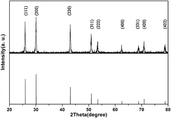
Phase composition and structure of pure PbS are characterized by XRD, and the profile is shown in Fig. 1. The XRD pattern demonstrates that all the peaks are well indexed and refer to PbS crystal of the cubic rock salt structure with the Fm3m space group. It is worth noting that the relative intensity of the {111} or {220} peaks to {200} peak is fairly greater than that standard PDF card depicts. This relative intensity variation suggests higher growth rate on the {111} and {110} facets, which is in good accordance with the exposure of {111} and {110} facets in truncated cubic PbS nanostructures.
XRD patterns of the as-prepared pure PbS nanostructures and the relative intensities of the diffraction peaks of standard PDF Card No. 05-0592.

In general, the nanocrystal size can be estimated using the Debye–Scherrer equation:
 $$D = k{\rm{\lambda }}/{\rm{\beta }}\cos \!{\rm{\theta }}\quad,$$
where D is crystallite diameter, k is a shape constant value of 0.9 here, λ is the x-ray wave length (1.5405 Å), β is the full width at half-maximum (FWHM) of the diffraction line, and θ is the diffraction angle in radian.Reference Rajesh, Mukundan, Pillai, Nair and Warrier30 The average size of pure PbS nanostructures is calculated to be 41 nm. Furthermore, the lattice constant is obtained from the pattern using software, which gives that a = 0.5943 nm that is slightly larger than the lattice constant of bulk PbS (0.5936 nm, PDF No. 05-0592).
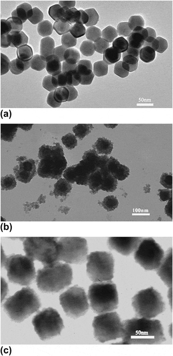
The morphology and size of the as-synthesized samples are assessed using TEM by dispersing proper quantities of samples in water and ultrasound for 10 min and then placing one drop of the dispersion on a grid. Figure 2 shows typical TEM images of the samples, which depict that the products exhibit essentially similar morphology and uniform size. Figure 2(a) is TEM image of pure PbS; it would seem that there are some nontruncated cubic agglomerations. The aggregating can be ascribed to the development of high index faces and increasing of the surface energy results from large surface to volume ratio. As shown in Fig. 2(b), it seems that the outer layers of ZnS are composed of much smaller crystallites, and the samples tend to grow into sphere-shaped particles. To the contrary, TEM image of CdS-encapsulated sample demonstrates a more uniform cubic and smooth surface as shown in Fig. 2(c), but no clear boundary is observed. Lattice mismatches between substrate PbS and epitaxial CdS, ZnS are main reason for the difference between Figs. 2(a) and 2(b) or 2(c).
TEM images of as-prepared (a) pure PbS, (b) ZnS encapsulated, and (c) CdS encapsulated.

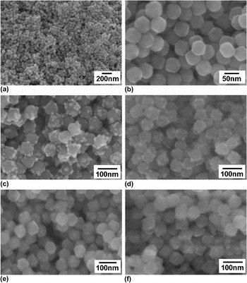
In this study, the scanning electron microscopy (SEM) observations are carried out to determine the morphology and chemical composition as shown in Fig. 3. It is seen that the nanocrystals have uniform shape anda particle size of 40–50 nm, which is in fairly good accordance with the calculated result. Figures 3(a) and 3(b) depict that the pure PbS nanostructures exhibit uniform truncated cubic shape with clear, clean, and smooth surface. But as for partly coated nanoparticles as Figs. 3(c)–3(f) shown, surface is partly coated with well-defined irregular spots, and the spacing and distribution of the spots are in a totally random manner with particle size hardly changes. Interestingly, it is hard to determine the difference in quantity and shape of spots on the four samples, but spots of Cd partly coated sample [Figs. 3(d) and 3(f)] tend to have a smaller size and a more uniform distribution. In contrast, ZnS partly coated samples exhibit larger spots size and some small spots agglomerate into a larger one.
SEM images of pure PbS with low (a) and high (b) magnification and PbS coated by (c) Zn 5%, (d) Zn 10%, (e) Cd 5%, and (f) Cd 10%.

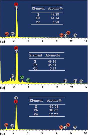
In addition, the energy dispersive spectroscopy (EDS) analysis is utilized to determine the chemical composition of the partly coated samples. EDS shows that these nanostructures have nearly stoichiometric composition, and the presence of Cd and Zn is observed (insets of Fig. 4). We can see from insets of Figs. 4(a) and 4(b) that the molar ratios of Zn and Cd to Pb, which are 13.5% and 11.5%, respectively, are fairly higher than the initial ratio, 10%, of the initial solution. This is dubious if you have noticed that the solubility product (Ksp) of PbS, ZnS, and CdS is 8 × 10⁻²⁸, 1.6 × 10⁻²⁴(wurtzite)/2.5 × 10−22(sphalerite), and 3.6 × 10⁻²⁹, respectively, and Kspa of PbS, ZnS, and CdS is 3 × 10⁻⁷, 3 × 10⁻²(wurtzite)/2 × 10−4(sphalerite), and 8 × 10⁻⁷, respectively.Reference Dean31, Reference Lide32 Difference in Ksp and Kspa means that the formation of CdS has priority to PbS and ZnS in neutral solution and the formation of PbS has priority in acidic solution. But taking excess TAA and products distribution into consideration, the utmost of Pb, Cd, and Zn ions is guaranteed because there is excess TAA, and meanwhile, ZnS and CdS mainly locate at the outer of a particle that facilitates reception of electron beam energy. So electron-induced characteristic x-ray emission of PbS would bear greater loss because of outer layer ZnS/CdS absorption and scattering, thus fairly higher molar ratio of Zn and Cd to Pb is observed. Comparison of Zn atomic percentage in Figs. 4(a) and 4(c) reveals that encapsulation can passivate nanostructures more efficiently. Given that the ZnS/CdS molar ratio is moderate relative to spots proportion, we presume that the spots consist of ZnS/CdS.
EDS spectra of PbS coated by (a) Zn 10%, (b) Cd 10%, and (c) PbS-encapsulated ZnS. The insets are EDS results of the samples.

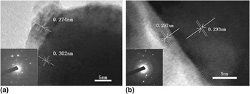
Considering that the composition of spots remains subject of hypotheses and conjectures, based only on fragmentary SEM observational evidence and indirect EDS analysis evidence, it is essential to carried out further measurements. To confirm the composition of surface spots of PbS nanostructures and to get further insight into the microstructure of the samples, HRTEM observation was carried out. As shown in Fig. 5, samples partly coated with ZnS and CdS exhibit disparate lattice parameter and morphology. Figure 5(a) shows that the interplanar spacings of ZnS partly coated PbS nanostructures are 0.302 and 0.274 nm, respectively, which are consistent with the separation of cubic PbS {200} planes and zinc blend ZnS {200} planes (PDF No. 05-0566). With the HRTEM image, we demonstrate that they consist of a uniform PbS core, surrounded by nonuniform spots of ZnS. Figure 5(b) shows the well-resolved lattice planes corresponding to a interplanar distance of 0.293 and 0.297 nm, which match very satisfactorily with both the spacings of PbS (200) planes and CdS (200) planes (PDF No. 65-2887). The high crystalline nature of the samples can also be determined by HRTEM images and selected area electron diffraction. The selected area electron diffractions of the samples are shown in the insets of Fig. 5. The clear spots, whether big or tiny, indicate that the samples are well crystallized.
HRTEM images of PbS coated by (a) Zn 10%, (b) Cd 10%. The insets were the selected area electron diffraction of the samples.

The HRTEM study mostly evidences two types of quite different morphologies. In Fig. 5(a), seemingly, ZnS nanocrystals with diameter of several nanometers adhere to the surface of PbS nanocrystals. However, the interface between spots and truncated cubic body in Fig. 5(b) is epitaxial with excellent transition, and the interfacial binding is more compact and uniform than ZnS partly coated samples do. It is envisaged that, because of the excess of TAA, PbS and ZnS would nucleate synchronously, but difference in the solubility product and greater concentration of Pb precursor gives growth of PbS priority. After the PbS nanocrystals grow up, unstable small ZnS clusters adhesive to PbS surface to form spots. As for CdS, because of similar Ksp, Kspa, and lattice constant, it is hard to deduce process of growth. We presume that the outside spots are consists of CdS because atomic ratio of Cd:Pb and Zn:Pb for the two samples are approximate in EDS quantification reports. The lattice of the PbS nanostructures is well developed, and the doping of Zn/Cd will increase free energy of the nanostructures just as quantum dots (QDs) do, so Zn and Cd tend to appear on the surface. Thus, HRTEM and EDS studies demonstrate that the samples contain both PbS and ZnS phase.
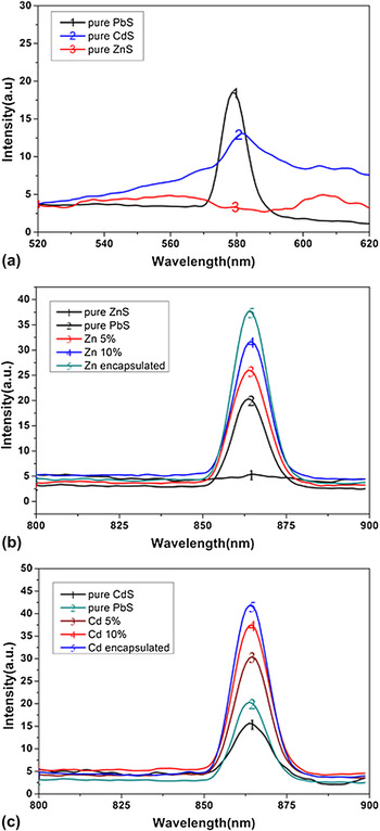
In case of semiconductor nanocrystals, the photoluminescence (PL) efficiency is strongly dependent on surface state and thus could be significantly improved by surface passivation.Reference Li, Wang, Guo, Keay, Mishima, Johnson and Peng33, Reference Wang, Long, Zhang, Zhong and Zhu34 In this work, it is probed via PL spectra measurements. The excitation spectra of pure PbS, ZnS, and CdS at excitation wave length of 863 nm are shown in Fig. 6(a). The emission spectra of obtained samples are shown in Figs. 6(b) and 6(c). As show in Figs. 6(b) and 6(c), partly coated samples with lower PL efficiency indicate poor surface passivation and PL efficiency increases as the atomic ratio of Cd/Pb rises. ZnS-encapsulated sample having the highest PL efficiency indicates improved surface passivation, and Zn-encapsulated curve in Fig. 6(b) is good collateral evidence. Similar results are obtained in the case of quantum dots where the phenomena are ascribed to the elimination of surface defects. So it is reasonable to get the conclusion that both CdS and ZnS can passivate PbS nanostructures efficiently. It can be seen that all the samples containing PbS perform different with pure ZnS and PbS, so partly coated samples could not be merely a mixture of PbS and ZnS/CdS. It is meaningful that the PL peak wave length of all as prepared samples is at 863 nm, which located in the so-called biological window between 600 and 1200 nm.Reference Waynant, Ilev and Gannot35 It would prove useful in expanding its biological applications.
(a) Excitation spectra of pure PbS, ZnS, and CdS and (b, c) emission spectra of the as-prepared samples at excitation wave length of 576 nm.

Ultraviolet–vis diffuse reflectance spectra are also measured for ZnS partly coated samples and KBr is used as a reference. The absorption edge, namely band gap of the bulk samples, is estimated indirectly using the equationReference Cheng, Huang, Dai, Qin, Zhang, Wang and Jiang36:
 $${\rm{\alpha }}hv = A(hv - E_{\rm{g}} )^{n/2}\quad ,$$
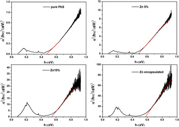
where α is absorption coefficient, hν is photon energy, E g is band gap, A is a constant, and the value of n for direct band gap semiconductor is 1. From (αhν)2 versus hν plot in Fig. 7, the optical absorption edge is estimated to be in the range of 0.47–0.58 eV. The optical properties of a material are governed by the interaction between the material and the electric field of optical wave. Electrons absorb energy of optical wave of particular frequencies and transition between their energy levels. Various types of transition such as the band-to-band transition, transition involving conduction band edge and surface, impurities, or defects states, give rise to different frequency dependencies of absorption coefficient near the optical absorption edge. The origin of unsmooth of plots may be elucidated by different transition types.Reference Kumar, Sharma, Zulfequar and Husain37
Plots of (αhν)2 versus hν for the band gap energies.

As an infrared (IR) transmitting material, ZnS transmits IR radiation rather good in the wave length range 570–14,700 nm,Reference Dean31 so it is meaningful to characterize electrical properties of ZnS partly coated samples. Permittivity also called dielectric constant is represented as a complex quantity in the following manner: ε = ε′+ iε″, where ε′ is the absolute permittivity divided by the permittivity of free space ε0, namely relative permittivity; ε″ is the imaginary permittivity describing energy loss. When an alternating electric field is applied, nanocrystals will be polarized and thus induce a capacitance current as well as a resistive current stems from free carriers. The resistive current will cause loss and is 90° advance of phase with respect to capacitance current, and the coangle between the resistive current and the total current is defined as δ. Dielectric loss factor defined as tgδ = ε″/ε′ is a more accurate and more scientific parameter to signify energy loss as well as the coupling strength between the nanocrystals and alternating electric field because molecular motion involved in polarization produces energy loss as well. Both permittivity and dielectric loss factor are dimensionless numbers.
Here, we present dielectric analysis of a ZnS partly coated sample and pure PbS. The sample nanoslides are dry pressed at 2 ton for 5 min, bottom coated with silver paste as electrode. By placing the sample under an alternative voltage and measuring the resulting current and the phase angle shift, real permittivity and dielectric loss factor of the sample nanoslides are determined. And parallel capacitance of the sample is measured directly. The real and imaginary parts of permittivity are given by the following equations:
 $${\rm{\varepsilon \prime}} = C_{\rm{m}} d/{\rm{\varepsilon }}_0 {\rm{\pi }}R^2 \quad,$$
 $${\rm{\varepsilon \Prime}} = {\rm{\varepsilon \prime tg\delta \quad,}}$$
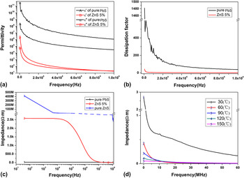
where C m is the parallel capacitance, d and R are the thickness and radius of the sample nanoslide, respectively, ε0 is the permittivity of free space. As Fig. 8(a) shows, both samples show a decrease of ε′ and ε″ with increasing frequency. At room temperature, compare to at 5 kHz, the real permittivity at 1 MHz decreases by a factor of about 7700 and 2800 for pure PbS and Zn 5% samples respectively. But the ε′ of PbS remains 30,700 at 1 MHz and it will continuously reduce to a number of 200 ± 35 in IR,Reference Cheng, Huang, Dai, Qin, Zhang, Wang and Jiang36 which is still 10 times greater than that of Zn 5% sample at 1 MHz. Finally, ε′, ε″, and tgδ reach a linear zone contributed by atomic and electronic polarization. In the lower frequency zone corresponds to permittivity representing the molecular dipole contribution, which decreases with increasing frequency, apparent peaks can be observed in the ε′ and ε″ curves of pure PbS, which could be more intuitively observed in curves of Fig. 8(b). The irregular peaks could be taken as signs of transition from dipole alignment to electronic and atomic polarization. For Zn 5% sample, no apparent abruptly increases and decreases and fairly low value of ε′ and ε″ originates from decreased polarity as a result of ZnS passivation. The decrease of ε″ at high frequency is not caused by fully achieved molecular motion involved in polarization. For Zn 5% sample, smooth ε′ and ε″ curves, one or several orders of magnitude lower value of ε′, ε″, and tgδ are all connected with passivation, which could decrease polarity of the material.
Real/imaginary permittivity (a), dielectric loss factor (b), impedance at different frequency (c), and impedance at different temperature (d) of the PbS coated by 5% ZnS.

The normalized impedance data shown in Fig. 8(c) are approximately monotonous over the observed range and show great frequency dependence as permittivity does. From Fig. 8(c), an initial region could be observed where the impedance of Zn 5% decreases slightly and is frequency independent but the value is thousand times bigger than that of pure PbS. The Zn 5% sample shows a zone around 1.5 MHz in which the impedance decreases dramatically, and as the frequency increased to 13 MHz, the impedance becomes smaller than that of pure PbS. The initial impedance of pure ZnS is tens of thousand times larger than that of Zn 5%. But the value drops dramatically with the increase of the frequency until about 15 MHz, and the descending branch can be divided into two different intervals, in a range of 40 to several thousands Hz and several thousands to about 15 MHz. Frequency difference in descending branch depicted different polarization. The two different descending of ZnS branches indicate space charge/electronic and ionic polarization mechanisms, respectively. Comparatively, the Zn 5% sample has only one descending interval, while pure PbS shows no descending branch. Differences in descending branches thus proclaim different material structure and composition. The downtrend of both curves could be well interpreted by theory of filter capacitor. These phenomena provide further proof about the existence of out layer ZnS. Temperature dependence of impedance is also invested. To minimize the influence of thermal hysteresis, the sample nanoslide is heated to 160 °C, and measurements are carried out during the temperature declining. Figure 8(d) indicates that the sample is very sensitive to heat, and the impedance of the ZnS 5% sample changes dramatically at lower frequency due to additional free carrier owing to thermal excitation.
IV. CONCLUSIONS
Uniform PbS nanostructures of varied morphology were prepared by a facile surfactant-assisted reflux route. ZnS and CdS layers were successfully coated onto PbS nanocrystals by encapsulation or epitaxial growth. By encapsulation, permittivity and dissipation of nanoslide were greatly decreased under ambient condition at whole frequency range (∼IR) due to the decreasing of polarity, but PL performance was enhanced because of surface passivation. Diffuse reflectance IR spectroscopy confirmed that the band gap can be tuned between 0.47 and 0.58 eV by partly coating. The interaction between the electron of outer layer ZnS and that of inner PbS caused stronger bound of conduction band electrons of PbS. The stronger bound of electrons may be responsible for the phenomenon above. To investigate difference in frequency characteristic and temperature characteristic of semiconductor nanoslides, high frequency measurements of permittivity together with temperature and frequency dependence of impedance investigations were performed. We demonstrate that the samples are thermal stable as well as get powerful collateral evidence of the existence of a ZnS heteroepitaxial layer. The method of measuring impedance to certify the existence of heterolayer is facile and can easily extended to other kinds of semiconductor. This work may prove useful in application developments such as NIR sensor and light signal amplification devices.
ACKNOWLEDGMENTS
This work was supported by projects from National Science Foundation of China (Grant No. 50972081), the Chinese PLA Medical Science and Technique Foundation (Grant No. CWS11J243), Independent Innovation Foundation of Shandong University (Grant No. IIFSDU 2011JC024), and the 111 Project (Grant No. B06017).