I. INTRODUCTION
The license-free allocated band at 60 GHz enables ultra-high rate wireless communications for commercial applications. Some of these application scenarios target mobile hand-held devices, e.g., purchase of high-definition videos with direct download to a mobile device. For this “data kiosk” or similar scenarios, cost and power consumption become an important design criterion at the receiver side where battery-operated, low-cost devices shall be used. In this respect, especially for data rates exceeding several gigabits-per-second, the cost and the power consumption of high-speed analog-to-digital converters (ADCs) with sufficient resolution are a considerable portion of the total cost and power consumption. Even for simple modulation formats, like single-carrier (SC) QPSK, a certain amount of oversampling and several bits of resolution are required for proper reception; whereas, as a rule of thumb, the power consumption of an ADC doubles for each increasing number of bits, and is linearly dependent on the sampling frequency [Reference Seyedi and Birru1].
This conflicting requirement of cost reduction while increasing the data rate motivates the investigation of alternate receiver architectures. For a classical “digital-oriented” super-heterodyne or homodyne receiver, the received signal at 60 GHz is downconverted to an intermediate frequency (IF) or to baseband, and then it is separated into its quadrature components. Afterwards, these components are converted to digital, and adjusted to the proper constellation in the digital domain.
II. RECEIVER CONCEPT
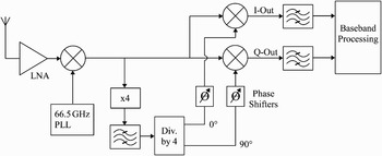
As an alternative to classical “digital-oriented” receivers, a highly hardware efficient “analog-oriented” receiver architecture is proposed. The schematic of the proposed receiver is shown in Fig. 1. The receiver is of super-heterodyne topology with an IF of 5 GHz. After the downconversion, the carrier signal at the IF is extracted from the modulated signal itself via a simple feed-forward carrier recovery concept suited for single-carrier (SC)-QPSK modulated signals. The recovered carrier is synchronous with the modulated signal; therefore, no additional constellation adjustment is required in the digital domain, eliminating the necessity of high precision ADCs. Moreover, the analog-frontend complexity of the proposed receiver is compatible with the more “classical” receivers, e.g. sliding-IF receiver [Reference Choi2], with the only additional frontend components being the frequency quadrupler, the bandpass, filter and the phase shifters. On the other hand, reducing the digital signal-processing load has also some drawbacks, like having no channel equalization, which limits the application scenarios to short distance line-of-sight (LOS) channel conditions (e.g. data-kiosk scenario).
Proposed synchronous receiver architecture.

The proposed carrier recovery concept is very simple and can be explained as follows. A QPSK modulated signal can be represented as

where S C(t) is the time variant amplitude function, m = 0, 1, 2, 3, and ω C and ϕ C(t) are the carrier frequency and phase to be recovered. Within the carrier recovery branch, the input QPSK signal is first frequency quadrupled resulting in:
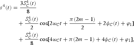
where φ 1 is the phase shift caused by the frequency quadrupling, and has a constant value. In the next step, the quadrupled signal is bandpass filtered centered at 4ω C, which reduces (2) to

Here φ 2 is the total phase shift caused by the frequency quadrupling and the bandpass filtering, whereas G C(t) represents the excess envelope fluctuations of the filtered signal, which is strongly dependent on the bandwidth of the bandpass filter being used. As within the argument of the cosine function − π = π = 3π = 5π, (3) reduces to

After frequency division by four, we obtain

As the frequency dividers are only sensitive to zero crossings, the envelope fluctuations are removed, and the resulting signal is the desired carrier with a constant phase shift of ϕ 3. Similar to the sliding-IF architecture, static frequency dividers can be used which provide the recovered carrier in quadrature components. In the final step of the carrier recovery, the phase shift ϕ 3 is corrected using phase shifters. Afterwards the recovered carrier is applied to the demodulators, and synchronous demodulated I and Q baseband bits are made available at the output of the receiver. The clock recovery is sufficiently handled at the baseband by the FPGA board; therefore this function has not been implemented in the analog front-end. Analog clock recovery circuits operating up to tens of gigabits data rates from optoelectronics field can be found in the literature [Reference Chan Ho, Dong Sik, Tae Gyu, Sang Kyu and Kang Wook3].
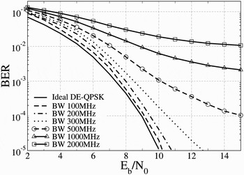
The presented receiver is suited for full monolithic integration, except for the carrier recovery bandpass filter centered at 20 GHz. From detailed system simulation results, which are shown in Fig. 2, it is concluded that the required bandwidth from the bandpass filter is much smaller than what could be achieved using on-chip components. The simulations are performed for an AWGN channel, with differentially encoded QPSK (DE-QPSK) signals, and root-raised-cosine pulse shaping filters with a roll-off factor of 0.3 in order to emulate band-limited transmission. Differential encoding is implemented in order to resolve the 90° phase ambiguity, whereas the detection method is still coherent. The phase ambiguity is an inherent problem of carrier tracking loops [Reference Simon4], and can be alternately resolved by implementing periodic synchronization sequences. On the other hand, the validity of the AWGN channel approximation is confirmed for the specific data-kiosk application scenario, and is discussed elsewhere [Reference Ulusoy, Liu, Peter, Fellbecker, Abdine and Schumacher5].
Simulated BER performance of the proposed receiver for different bandpass filters.

As seen in Fig. 2, for sufficiently sharp bandpass filters the simulated BER performance of the proposed receiver is close to the ideal DE-QPSK curve. However, for bandwidth values that are larger than 500 MHz, BER floors are observed, indicating that the recovered carrier jitters. A bandpass filter with a 3 dB bandwidth of 500 MHz already requires a quality factor of 40, and cannot be implemented on chip. In keeping with the cost budget, it is implemented as part of the package (system on package (SoP)).
A further consideration for the proposed receiver is the influence of phase noise on the overall system performance. Due to the feed-forward carrier recovery, the phase noise of the recovered carrier is coherent with the phase noise of the modulated signal, which adds a significant degree of phase noise suppression [Reference Noe6]. This additional feature of the proposed hardware-efficient receiver was also investigated with system level simulations [Reference Ulusoy, Liu, Peter, Fellbecker, Abdine and Schumacher5]. The phase noise coherence between the recovered carrier and the modulated signal is highly dependent on the true time delay shift caused by the carrier recovery branch. As the value of the delay shift gets larger, the degree of phase noise suppression is reduced. Nevertheless, it is concluded that still a significant amount of phase noise suppression can be achieved without any delay compensation, and for the implementation of the receiver phase compensation instead of delay compensation is preferred.
All the active components of the receiver are realized in 0.8 µm Telefunken semiconductors SiGe2RF HBT technology (f T and f max ≈ 80 GHz) leaving out the LNA, which cannot be realized in an 80 GHz technology. The LNA is realized in 0.25 µm IHP SG25H1 BiCMOS technology, which is again to be integrated on the same final package. For the first prototype implementation, monolithic integration is performed in two separate blocks, namely, the 60 GHz/5 GHz downconverter and the synchronous IF demodulator. The realized monolithic integrated receiver blocks experimentally demonstrate the simple synchronous reception concept for data rates up to 3.5 G Bit/s, and that it is possible to implement millimeter-wave frontends with low-cost technologies (f op/f max ~ 0.75). The detailed description of the receiver blocks will be presented in the following.
III. DOWNCONVERTER
A) LNA
As previously mentioned, the LNA is realized as a separate chip in IHP SG25H1 technology (f max ≈ 220 GHz). The IC is designed by TES Electronic solutions, Stuttgart [7]. It is a differential LNA in two-stage cascode topology, and exhibits a measured gain of 26 dB with a simulated noise figure of 6.9 dB. The LNA is to be glued on the same carrier substrate with the hardware efficient receiver ICs and wire bonded to the input of the monolithic integrated downconverter IC. More details of the LNA circuit can be found in [Reference Grujić, Savić, Bingöl and Saranovac8].
B) Downconversion mixer
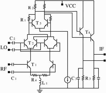
The downconversion mixer is a modified Gilbert-cell structure, whose schematic is shown in Fig. 3. The ground-side current source is replaced by an inductor, which is a customary modification for millimeter-wave Gilbert-cell mixers. A transimpedance amplifier (transistors T3) is cascaded with the switching quad (transistors T2). This improves gain and enhances bandwidth due to the low load impedance presented to the switching quad [Reference Johansen, Vidkjaer and Krozer9]. The output is buffered with common collector stages, and R 3 and C 3 implement capacitive emitter peaking to further enhance the bandwidth. The realized mixer has an IF-bandwidth exceeding 10 GHz which is sufficient to downconvert multi-Gbps broadband signals.
Simplified schematic of the designed downconversion mixer. R 1 = 400 Ω, R 2 = 300 Ω, R 3 = 480 Ω, R 4 = 24 Ω, C 1 = 0.3 pF, C 2 = 0.5 pF, C 3 = 0.33 pF and L 1 = 0.5 nH.

C) VCO
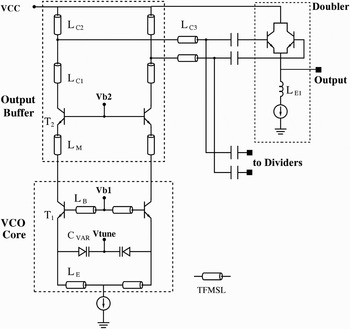
In Fig. 4, the simplified schematic of the realized VCO is displayed. The fully differential local oscillator is operational at 1/2 the frequency and its output is connected to a push–push frequency doubler. The reactive components are realized with thin film microstrip lines (TFMSL), using the top metal as the signal line and the bottom metal as the ground. The core VCO has a large tuning range of 32–42 GHz, an output power of 7 dBm whereas the phase noise spectral power density was measured at −90 dBc/Hz at 1 MHz offset from the carrier. The frequency doubler consists of emitter coupled pair transistors. When the input is fed differentially, a strong second harmonic is generated at the emitter node serving as the output. At the doubler output, the frequency can be tuned from 64 to 83 GHz and the output power is around −6 dBm at 68 GHz. A more detailed description of the VCO can be found in [Reference Liu, Ulusoy, Trasser and Schumacher10].
Simplified schematic of the designed VCO and the push–push frequency doubler. L C1 = 100 µm, L C2 = 120 µm, L C3 = 100 µm, L M = 100 µm, L B = 250 µm, L E = 800 µm and L E1 = 0.5 nH.

D) Monolithic integrated downconverter
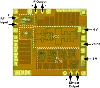
In Fig. 5, the chip-photo of the realized frequency down converter is shown. Apart from the already discussed VCO, doubler and mixer, the IC features a 32:1 frequency divider containing two dynamic and three static divider sections, and a phase-locked loop circuit that locks the emission to a 1.04 GHz reference signal. The chip is very compact, and occupies an area of 1.18 × 1.07 mm2, including the bond pads. The MMIC is supplied from two DC sources, drawing 120 mA from a 3.5 V DC voltage source, and 4 mA from a 4 V DC voltage source.
Chip photograph of the monolithic integrated downconverter.

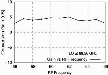
The complete downconverter is characterized on-wafer. The RF input signal is fed single ended and is swept from 56 to 66 GHz covering the whole ISM band, whereas the IF output is probed with a differential GSSG probe. The measured downconversion gain for an LO frequency of 66.56 GHz is shown in Fig. 6. The intended RF input frequency is 61.56 GHz resulting in an IF of 5 GHz. A high-lying LO frequency is preferred owing to the better phase noise performance of the core VCO at the corresponding half frequency. As seen in Fig. 6, the downconverter exhibits a conversion gain of around 5 dB, whereas the 3 dB IF bandwidth equals 12 GHz. The measured 1 dB input compression point of the downconverter equals −10 dBm.
Measured conversion gain of the downconverter for swept RF frequency from 56 to 66 GHz and fixed LO frequency at 66.56 GHz.

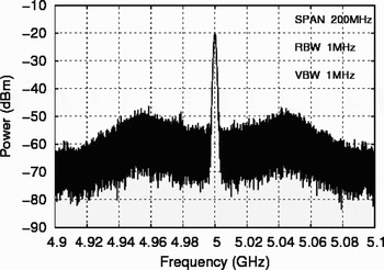
In Fig. 7, the downconverted spectrum at 5 GHz for a span of 200 MHz is displayed, showing a PLL loop bandwidth of approximately 60 MHz.
Measured downconverted spectrum at 5 GHz.

The simulated SSB NF of the downconverter equals 28 dB. If 3 dB interconnect losses are assumed, when integrated on-package with the presented LNA, still a tolerable noise figure of around 11 dB would be achieved for the whole system, whereas the influence of the downconverter would still be negligible. The use of a low-cost technology with 80 GHz f T is hence possible for short-range 60 GHz data links, with an addition of off-the-shelf LNA where needed. To maintain the cost advantage, a cost-efficient packaging approach will have to be used and is equally explored as part of the project.
IV. SYNCHRONOUS IF DEMODULATOR
A) Frequency quadrupler
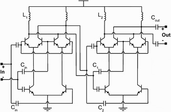
The simplified schematic of the designed frequency quadrupler is shown in Fig. 8. The frequency quadrupler consists of two modified Gilbert-cell mixers operated as squaring devices. The output of the first mixer is matched to the input of the second one at 10 GHz, whereas the output of the second mixer is matched to a 100 Ω differential load at 20 GHz. By this means, a tuned behavior with an input frequency of 5 GHz and an output frequency of 20 GHz is achieved. The measured 3 dB bandwidth extends from 19 to 22.2 GHz at the output with a conversion gain of 0.5 dB at an input power of −9 dBm [Reference Ulusoy, Liu, Trasser and Schumacher11].
Simplified schematic of the designed frequency quadrupler. C in = 2 pF, L 1 = 0.51 nH, C 1 = 1 pF, C 2 = 0.4 pF, L 2 = 0.2 nH and C out = 0.2 pF.

B) Divide-by-four frequency divider
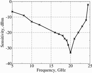
The divide-by-four frequency divider consists of two stacked divide-by-two static frequency dividers in master–slave flip-flop topology. The input sensitivity of the designed frequency divider is matched to 20 GHz in consideration of the potentially low power levels at the input due to the carrier recovery and the external BPF losses. Furthermore, in order to properly interface the external BPF, one of the inputs of the divider is matched to 50 Ω by inserting a series inductor. The measured single-ended sensitivity of the realized divider, displayed in Fig. 9, shows that the desired sensitivity behavior is achieved, and the designed divider is well suited for the carrier recovery application.
Single-ended sensitivity measurement of the realized divide-by-four static frequency divider.

C) Bandpass filter
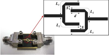
Figure 10 shows the photograph and layout of the realized filter. The substrate material is RT/Duroid 5880, which will also hold the receiver ICs and the 60 GHz antenna. The thickness of the material is 128 µm with an ɛ r of 2.2.The designed filter utilizes transmission zeros, and has a simple, highly compact structure, which can easily be integrated on the final package. The transmission zeros are generated by asymmetric tapping of the filter resonators, resulting in two λ/4 transformers, L 1 and L 2, which convert the open ended transmission lines to shorts at the feed taps. At the center frequency, the sum of L 1 and L 2 equals λ/2, and the bandwidth of the filter is determined by adjusting the location of the transmission zeros.
Layout and photograph of the realized BPF. L 1 = 2.64 mm, L 2 = 2.24 mm, S = 0.38 mm, d = 1.1 mm and linewidth = 0.35 mm.

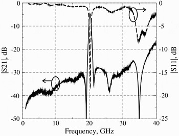
The measured S-parameters of the realized filter are displayed in Fig. 11 showing the transmission zeros at 19.1 and 21.2 GHz, while the filter is centered at 20.1 GHz with a 3 dB bandwidth of 520 MHz (2.6% relative). The measured insertion loss of the filter equals 4.6 dB including the connector losses, which is estimated to be in total 1.6 dB by a through line measurement. The designed filter is well suited for the application in question, and using the same structure, bandwidth values down to 300 MHz can be achieved without excessive insertion loss.
Measured S-parameters of the realized BPF.

D) Phase shifter
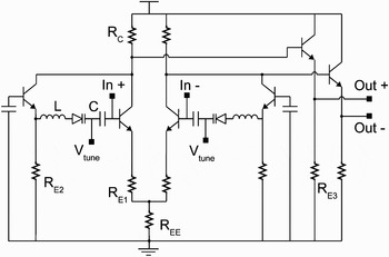
Although the required phase correction for the carrier recovery has a constant predetermined value, for the prototype implementation, a tunable active phase shifter in all pass filter topology is realized. The simplified schematic is shown in Fig. 12. The realized circuit acts as a second order APF, with a resonant frequency ω n of  [Reference Zhou, Safarian and Heydari12]. The capacitor C is realized as a combination of an MIM capacitor and a varactor diode, acquiring a tunable behavior.
Simplified schematic of the designed active phase-shifter. R C = 100 Ω, R E1 = 100 Ω, R E2 = 30 Ω, R E3 = 350 Ω, R EE = 100 Ω, L = 0.5 nH, C = 0.4 pF.

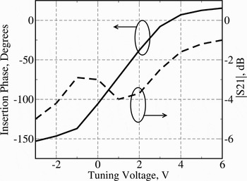
In Fig. 13, the measured phase and magnitude response of the realized APF is shown at 5 GHz for varying tuning voltage. As shown, a phase tuning range of above 150° is achieved for a magnitude variation of 4 dB, sufficient for the carrier recovery.
Measured magnitude and phase response of the realized APF.

E) Demodulator
The designed demodulators are in standard Gilbert-cell mixer topology, where the recovered carrier is applied to the upper switching-quad transistors, and the modulated signal is applied to the lower transconductance-pair transistors. The measured downconversion gain of the demodulators is 1 dB, the input 1 dB compression point is 0 dBm and the measured output bandwidth ranges from DC to 3.8 GHz, which is sufficient to demodulate data rates up to 5.5 Gbit/s as a rule of thumb.
F) Monolithic integrated synchronous IF demodulator
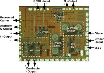
The chip-photo of the realized synchronous IF demodulator is shown in Fig. 14. The MMIC consists of the frequency quadrupler, the divide by four static frequency divider, two active phase shifters and two demodulators. The area consumption is 1.7×2.1 mm2, and the power consumption is 110 mA from a single 2.5 V DC voltage supply. Following the previously described carrier recovery concept, the MMIC receives QPSK-modulated signals as input and delivers the synchronously demodulated quadrature baseband bits as output, provided that the output of the quadrupler is connected to the input of the divider through the external bandpass filter.
Chip photograph of the monolithic integrated synchronous IF demodulator.

The synchronous IF demodulator is tested on-wafer. The pad configuration of the designed MMIC is arranged in a way that allows on-wafer characterization with an external bandpass filter. For proper testing of the carrier recovery and synchronous demodulation, ultra-high rate modulated IF QPSK test signals are required. Due to the lack of such high data rate signal generators, a custom BPSK modulator is designed. BPSK modulation is preferred because it simplifies the design of the custom modulator, and BPSK modulated test signals can serve as a proof of concept for the QPSK carrier recovery.
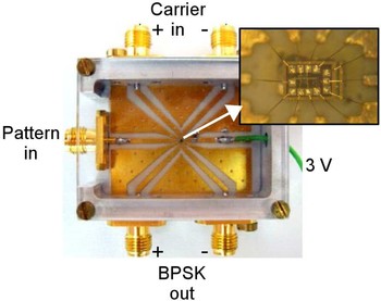
The photograph of the realized custom modulator is shown in Fig. 15. The custom modulator is a simple Gilbert-cell mixer similar to the previously described demodulators. In order to operate as a modulator, the mixer is designed to have an extended output bandwidth of 13 GHz. The custom modulator receives the 5 GHz carrier signal and data pattern as input, and delivers BPSK-modulated signal as output.
Photograph of the realized custom BPSK modulator.

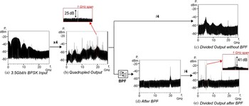
In Fig. 16 the measured spectrum after each step of the carrier recovery is shown. The input BPSK signal is generated using the presented custom modulator, by applying a differential 5 GHz carrier signal, and a pseudorandom bit-sequence of 3.5 Gbit/s data rate. The single-ended measured spectrum of the generated BPSK signal is displayed in Fig. 16(a). As seen in Fig. 16(b), the frequency quadrupling generates a strong carrier component at 20 GHz with spurious components. An important observation is that the strongest spurious components are at a distance equal to the symbol rate, whereas the spurious components in the close vicinity of the carrier component have relatively low power with a measured suppression of 25 dB. This feature makes the presented carrier recovery especially suited for higher data rates. It is clear that the resulting time domain signal after frequency quadrupling is not a clean periodic signal, and direct frequency division is not possible. This is shown in Fig 16(c), without filtering the dividers generate a very noisy output at around 5 GHz, which cannot be used for demodulation. On the other hand, after bandpass filtering, the spectrum is sufficiently cleaned up, and the frequency dividers are able to lock to the carrier component generating a clean output shown in Fig 15(e). Due to the insensitivity of the dividers to envelope fluctuations, the suppression of the spurious component have increased to 41 dB as shown in the inset for a 1 GHz span. The recovered carrier with the designed filter is stable and modulation free, and suited for synchronous demodulation.
Measured spectrum after each step of the carrier recovery.

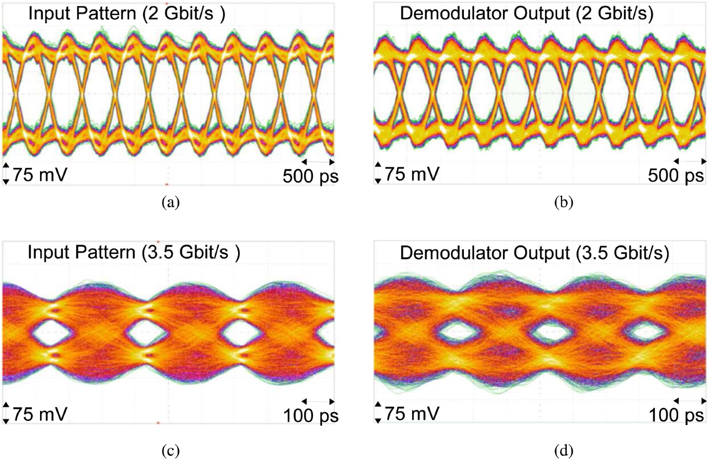
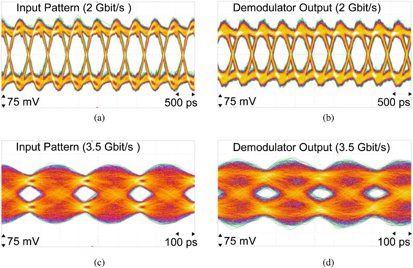
The synchronous demodulation is confirmed by measuring the demodulator outputs, after applying the required tuning voltage to the phase shifters. Once the phase shift is properly adjusted, the receiver becomes insensitive to the frequency and/or phase changes of the input signal. The measured eye diagrams of the demodulated bit sequence for 2 and 3.5 Gbit/s data rates are shown in Fig. 17. The output of the demodulators are filtered with commercial low-pass filters with a 3 dB corner frequency of 1.75 GHz. As seen in Fig. 17(b), for 2 Gbit/s data rate the signal quality is very high, demonstrating the successful principle operation of the presented synchronous demodulator. On the other hand for 3.5 Gbit/s data rate, shown in Fig. 17(d), strong distortions of the measured eye diagram are observed. These distortions are dominated by the commercial low-pass filters used at the output of the MMIC. The filters have a non-constant group-delay response with strong peaking behavior, which causes inter-symbol interference and distorts the output pattern. In order to further demonstrate this effect, in Figs 17(a) and 17(c), the eye diagrams of the input patterns that are directly measured from the pattern generator through the commercial low-pass filters are displayed. When compared to Figs 17(b) and 17(d), it can be concluded that the synchronous QPSK demodulator achieves successful demodulation, and most of the distortion is caused by the commercial low-pass filters, which also prevent testing higher data rates.
Measured eye diagrams of the synchronously demodulated bit-patterns at 2 and 3.5 Gbit/s data rates. The 3.5 Gbit/s results are strongly affected by the commercial low-pass filters.
V. CONCLUSION
In this paper, a hardware efficient receiver concept is presented, performing synchronous demodulation of Gbit/s BPSK and QPSK signals in the analog domain. Successful downconversion of 60 GHz signals to a 5 GHz IF, and synchronous demodulation of BPSK signals at 3.5 Gbit/s is demonstrated.
The described method eliminates the need for power hungry large bandwidth, high precision ADCs. The works also indicates that short-range wireless communication devices at 60 GHz may be well fabricated using very inexpensive technologies.
ACKNOWLEDGEMENT
This work was supported by the German Federal Ministry of Education and Research in the framework of the R&D initiative: “Enablers for Ambient Services and Systems, Part A - 60 GHz Broadband Links” (EASY-A).
 Ahmet Çağrı Ulusoy received his B.Sc. in electronics engineering in 2006 from Istanbul Technical University, Istanbul, Turkey. He continued his studies with an M.Sc. degree in Communications Technology in Ulm University, where he is currently working on his doctoral degree in the Institute of Electron Devices and Circuits. His research area covers low-cost mm-wave communications, MMIC and planar circuit design.
 Gang Liu received his bachelor degree in electrical engineering in 2005 from Shandong University, China and master degree in Communications Technology in 2007 from University of Ulm, Germany. Since 2007, he started working towards his Ph.D. degree at Institute of Electron Devices and Circuits, University of Ulm, Germany. His main research topic is mm-wave Circuit design with SiGe HBTs.
 Andreas Trasser received his Ph.D. degree in 1989 from RWTH Aachen, Aachen, Germany. He joined the Institute of Electron Devices and Circuits in Ulm University in 1990, where he currently is a member of the academic staff and lecturer. His research interests are mainly focused on the design of analog circuits.
 Hermann Schumacher received his doctorate in engineering (Dr.-Ing.) from RWTH Aachen, Aachen, Germany in 1986. After working for Bellcore, Redbank, NJ, from 1986 to 1990, he joined Ulm University as a professor in the School of Engineering and Computer Engineering. He is currently the director of the Institute of Electron Devices and Circuits, and the director of the Communications Technology international M.Sc. program.
His research interests range from compound semiconductor devices for micro- and mm-wave applications to high-frequency microsystems, including low-cost mm-wave communication solutions and impulse-radio ultra-wideband techniques for biomedical sensing.